EP1434099B1 - Verfahren zur Herstellung einer Vorrichtung - Google Patents
Verfahren zur Herstellung einer Vorrichtung Download PDFInfo
- Publication number
- EP1434099B1 EP1434099B1 EP20030257415 EP03257415A EP1434099B1 EP 1434099 B1 EP1434099 B1 EP 1434099B1 EP 20030257415 EP20030257415 EP 20030257415 EP 03257415 A EP03257415 A EP 03257415A EP 1434099 B1 EP1434099 B1 EP 1434099B1
- Authority
- EP
- European Patent Office
- Prior art keywords
- aberrations
- mask
- pattern
- different
- imaging
- Prior art date
- Legal status (The legal status is an assumption and is not a legal conclusion. Google has not performed a legal analysis and makes no representation as to the accuracy of the status listed.)
- Expired - Lifetime
Links
- 238000004519 manufacturing process Methods 0.000 title claims description 8
- 230000004075 alteration Effects 0.000 claims description 63
- 238000000034 method Methods 0.000 claims description 39
- 230000000694 effects Effects 0.000 claims description 35
- 239000000758 substrate Substances 0.000 claims description 34
- 230000005855 radiation Effects 0.000 claims description 27
- 239000006096 absorbing agent Substances 0.000 claims description 21
- 238000003384 imaging method Methods 0.000 claims description 21
- 238000005286 illumination Methods 0.000 claims description 20
- 230000035945 sensitivity Effects 0.000 claims description 17
- 201000009310 astigmatism Diseases 0.000 claims description 13
- 230000008569 process Effects 0.000 claims description 8
- 239000000463 material Substances 0.000 claims description 7
- 206010010071 Coma Diseases 0.000 claims description 5
- 238000004590 computer program Methods 0.000 claims description 5
- 238000004364 calculation method Methods 0.000 claims description 2
- 238000012937 correction Methods 0.000 description 19
- 230000006870 function Effects 0.000 description 14
- 239000010410 layer Substances 0.000 description 13
- 238000000059 patterning Methods 0.000 description 12
- 239000011295 pitch Substances 0.000 description 12
- 238000006073 displacement reaction Methods 0.000 description 9
- 230000003287 optical effect Effects 0.000 description 8
- 230000001419 dependent effect Effects 0.000 description 7
- 230000004044 response Effects 0.000 description 5
- 238000004088 simulation Methods 0.000 description 5
- 230000006872 improvement Effects 0.000 description 4
- 230000010363 phase shift Effects 0.000 description 4
- 238000010586 diagram Methods 0.000 description 3
- 238000009826 distribution Methods 0.000 description 3
- 238000007654 immersion Methods 0.000 description 3
- VYZAMTAEIAYCRO-UHFFFAOYSA-N Chromium Chemical compound [Cr] VYZAMTAEIAYCRO-UHFFFAOYSA-N 0.000 description 2
- ZOKXTWBITQBERF-UHFFFAOYSA-N Molybdenum Chemical compound [Mo] ZOKXTWBITQBERF-UHFFFAOYSA-N 0.000 description 2
- XUIMIQQOPSSXEZ-UHFFFAOYSA-N Silicon Chemical compound [Si] XUIMIQQOPSSXEZ-UHFFFAOYSA-N 0.000 description 2
- 238000005516 engineering process Methods 0.000 description 2
- 239000007788 liquid Substances 0.000 description 2
- 238000001459 lithography Methods 0.000 description 2
- 229910052750 molybdenum Inorganic materials 0.000 description 2
- 239000011733 molybdenum Substances 0.000 description 2
- 229910052710 silicon Inorganic materials 0.000 description 2
- 239000010703 silicon Substances 0.000 description 2
- 230000003068 static effect Effects 0.000 description 2
- 229910052715 tantalum Inorganic materials 0.000 description 2
- GUVRBAGPIYLISA-UHFFFAOYSA-N tantalum atom Chemical compound [Ta] GUVRBAGPIYLISA-UHFFFAOYSA-N 0.000 description 2
- 101100545229 Saccharomyces cerevisiae (strain ATCC 204508 / S288c) ZDS2 gene Proteins 0.000 description 1
- 101100113084 Schizosaccharomyces pombe (strain 972 / ATCC 24843) mcs2 gene Proteins 0.000 description 1
- 229910004535 TaBN Inorganic materials 0.000 description 1
- 101100167209 Ustilago maydis (strain 521 / FGSC 9021) CHS8 gene Proteins 0.000 description 1
- 238000010521 absorption reaction Methods 0.000 description 1
- 230000003044 adaptive effect Effects 0.000 description 1
- 238000004458 analytical method Methods 0.000 description 1
- 238000003491 array Methods 0.000 description 1
- 230000002238 attenuated effect Effects 0.000 description 1
- 229910052790 beryllium Inorganic materials 0.000 description 1
- ATBAMAFKBVZNFJ-UHFFFAOYSA-N beryllium atom Chemical compound [Be] ATBAMAFKBVZNFJ-UHFFFAOYSA-N 0.000 description 1
- 230000008859 change Effects 0.000 description 1
- 230000001143 conditioned effect Effects 0.000 description 1
- 238000001514 detection method Methods 0.000 description 1
- 230000009977 dual effect Effects 0.000 description 1
- 230000005670 electromagnetic radiation Effects 0.000 description 1
- 238000002474 experimental method Methods 0.000 description 1
- 238000001900 extreme ultraviolet lithography Methods 0.000 description 1
- 239000012530 fluid Substances 0.000 description 1
- 238000007689 inspection Methods 0.000 description 1
- 230000003993 interaction Effects 0.000 description 1
- 239000002346 layers by function Substances 0.000 description 1
- 239000004973 liquid crystal related substance Substances 0.000 description 1
- 230000005381 magnetic domain Effects 0.000 description 1
- 239000011159 matrix material Substances 0.000 description 1
- 230000015654 memory Effects 0.000 description 1
- QSHDDOUJBYECFT-UHFFFAOYSA-N mercury Chemical compound [Hg] QSHDDOUJBYECFT-UHFFFAOYSA-N 0.000 description 1
- 229910052753 mercury Inorganic materials 0.000 description 1
- 230000004048 modification Effects 0.000 description 1
- 238000012986 modification Methods 0.000 description 1
- 238000010606 normalization Methods 0.000 description 1
- 238000005457 optimization Methods 0.000 description 1
- 230000008092 positive effect Effects 0.000 description 1
- 238000012545 processing Methods 0.000 description 1
- 210000001747 pupil Anatomy 0.000 description 1
- 238000007493 shaping process Methods 0.000 description 1
- 238000004513 sizing Methods 0.000 description 1
- 230000003595 spectral effect Effects 0.000 description 1
- 238000010561 standard procedure Methods 0.000 description 1
- 239000010409 thin film Substances 0.000 description 1
- 229910052720 vanadium Inorganic materials 0.000 description 1
- XLYOFNOQVPJJNP-UHFFFAOYSA-N water Substances O XLYOFNOQVPJJNP-UHFFFAOYSA-N 0.000 description 1
Images


Classifications
-
- B—PERFORMING OPERATIONS; TRANSPORTING
- B82—NANOTECHNOLOGY
- B82Y—SPECIFIC USES OR APPLICATIONS OF NANOSTRUCTURES; MEASUREMENT OR ANALYSIS OF NANOSTRUCTURES; MANUFACTURE OR TREATMENT OF NANOSTRUCTURES
- B82Y10/00—Nanotechnology for information processing, storage or transmission, e.g. quantum computing or single electron logic
-
- B—PERFORMING OPERATIONS; TRANSPORTING
- B82—NANOTECHNOLOGY
- B82Y—SPECIFIC USES OR APPLICATIONS OF NANOSTRUCTURES; MEASUREMENT OR ANALYSIS OF NANOSTRUCTURES; MANUFACTURE OR TREATMENT OF NANOSTRUCTURES
- B82Y40/00—Manufacture or treatment of nanostructures
-
- G—PHYSICS
- G03—PHOTOGRAPHY; CINEMATOGRAPHY; ANALOGOUS TECHNIQUES USING WAVES OTHER THAN OPTICAL WAVES; ELECTROGRAPHY; HOLOGRAPHY
- G03F—PHOTOMECHANICAL PRODUCTION OF TEXTURED OR PATTERNED SURFACES, e.g. FOR PRINTING, FOR PROCESSING OF SEMICONDUCTOR DEVICES; MATERIALS THEREFOR; ORIGINALS THEREFOR; APPARATUS SPECIALLY ADAPTED THEREFOR
- G03F1/00—Originals for photomechanical production of textured or patterned surfaces, e.g., masks, photo-masks, reticles; Mask blanks or pellicles therefor; Containers specially adapted therefor; Preparation thereof
- G03F1/22—Masks or mask blanks for imaging by radiation of 100nm or shorter wavelength, e.g. X-ray masks, extreme ultraviolet [EUV] masks; Preparation thereof
- G03F1/24—Reflection masks; Preparation thereof
-
- G—PHYSICS
- G03—PHOTOGRAPHY; CINEMATOGRAPHY; ANALOGOUS TECHNIQUES USING WAVES OTHER THAN OPTICAL WAVES; ELECTROGRAPHY; HOLOGRAPHY
- G03F—PHOTOMECHANICAL PRODUCTION OF TEXTURED OR PATTERNED SURFACES, e.g. FOR PRINTING, FOR PROCESSING OF SEMICONDUCTOR DEVICES; MATERIALS THEREFOR; ORIGINALS THEREFOR; APPARATUS SPECIALLY ADAPTED THEREFOR
- G03F7/00—Photomechanical, e.g. photolithographic, production of textured or patterned surfaces, e.g. printing surfaces; Materials therefor, e.g. comprising photoresists; Apparatus specially adapted therefor
- G03F7/70—Microphotolithographic exposure; Apparatus therefor
- G03F7/70216—Mask projection systems
- G03F7/70283—Mask effects on the imaging process
-
- G—PHYSICS
- G03—PHOTOGRAPHY; CINEMATOGRAPHY; ANALOGOUS TECHNIQUES USING WAVES OTHER THAN OPTICAL WAVES; ELECTROGRAPHY; HOLOGRAPHY
- G03F—PHOTOMECHANICAL PRODUCTION OF TEXTURED OR PATTERNED SURFACES, e.g. FOR PRINTING, FOR PROCESSING OF SEMICONDUCTOR DEVICES; MATERIALS THEREFOR; ORIGINALS THEREFOR; APPARATUS SPECIALLY ADAPTED THEREFOR
- G03F7/00—Photomechanical, e.g. photolithographic, production of textured or patterned surfaces, e.g. printing surfaces; Materials therefor, e.g. comprising photoresists; Apparatus specially adapted therefor
- G03F7/70—Microphotolithographic exposure; Apparatus therefor
- G03F7/70483—Information management; Active and passive control; Testing; Wafer monitoring, e.g. pattern monitoring
- G03F7/70591—Testing optical components
- G03F7/706—Aberration measurement
Definitions
- the present invention relates to a device manufacturing method using a lithographic apparatus and to computer programs for use in controlling lithographic apparatus.
- a lithographic apparatus is a machine that applies a desired pattern onto a target portion of a substrate.
- Lithographic apparatus can be used, for example, in the manufacture of integrated circuits (ICs).
- a patterning means such as a mask, may be used to generate a circuit pattern corresponding to an individual layer of the IC, and this pattern can be imaged onto a target portion (e.g. comprising part of, one or several dies) on a substrate (e.g. a silicon wafer) that has a layer of radiation-sensitive material (resist).
- a single substrate will contain a network of adjacent target portions that are successively exposed.
- lithographic apparatus include so-called steppers, in which each target portion is irradiated by exposing an entire pattern onto the target portion in one go, and so-called scanners, in which each target portion is irradiated by scanning the pattern through the projection beam in a given direction (the "scanning"-direction) while synchronously scanning the substrate parallel or anti-parallel to this direction.
- EUV extreme ultraviolet radiation
- the mask must be formed as a distributed Bragg reflector formed by a multilayer of 40 or more layer pairs of, for example, (Mo/Si) or (Mo/Be).
- the mask pattern is then formed by an overlying patterned absorber layer such as Tantalum (Ta) or Chrome (Cr).
- the multilayer and absorber layer must be relatively thick, many tens of wavelengths, and this, coupled with the necessity to illuminate the mask obliquely, introduces various errors in the projected image, as compared to an ideal, thin binary mask.
- EP-1 251 402-A discloses the idea of deliberately introducing aberrations into a projection lens to compensate for other aberrations already present so as to minimize a merit function. Also disclosed is to compensate for Bossung tilt deriving from deviations from the correct 180° phase shift in a phase-shift mask (PSM)
- PSM phase-shift mask
- a thick absorber for use with EUV radiation may, for example, have a thickness of 50-100nm or more.
- the invention uses any available "knobs" in the projection system to effect wavefront or phase manipulation to correct any correctables in the image shape. This assists in bringing process windows for different features closer together. It is also possible to use iso-focal tilt as the metric for level of aberration input and reduce the differences between different structure types. The choice of metric is important as improvement in isofocal tilt may worsen best focus shift performance, and vice versa.
- the method of the present invention can also compensate for mask-induced image CD offset, which occurs as a function of mask angle of incidence (MAI), absorber thickness, feature type and NA/illumination settings.
- MAI mask angle of incidence
- absorber thickness absorber thickness
- feature type and NA/illumination settings.
- the dominant effect is a CD variation between features as a function of structural orientation, for example a horizontal-vertical (HV) bias varying across the image field.
- HV horizontal-vertical
- the mask will induce ellipticity variation across the image field.
- the low order system aberrations are Z5 astigmatism, Z9 spherical, and Z12 astigmatism (as defined below) or equivalent aberrations.
- Simulations of dense and semi-isolated structures, with and without aberrations, have provided sensitivity data for best focus (BF) shift and isofocal tilt (IFT).
- Optimized combinations of Zernikes Z5, Z9 and Z12 can compensate for, and reduce, best focus shifts and isofocal tilt to bring focus positions of dense, semi-isolated, horizontal and vertical lines of same critical dimension (CD) closer together.
- CD critical dimension
- Contact hole ellipticity variation across the image field can be compensated for using mostly Z5 astigmatism.
- HV bias variation can be compensated for in combination with best focus shift and iso-focal tilt using principally combinations of Z5, Z9 and Z12 aberrations.
- a further problem that the invention may address is image displacement in the XY plane. Such displacements may occur as a function of mask angle of incidence, absorber thickness, feature type and NA/illumination settings and the displacements will be dependent on position in the image field. Whilst such effects may be compensated for in some cases by pre-distortion of the mask and by optical proximity corrections, these solutions tie the mask to use with a particular set of machine settings.
- a more flexible solution can be provided by the invention by controlling and/or introducing projection system aberrations, particularly Z2, Z3, and Z7 (as defined below).
- a further aspect of the present invention provides a method and computer program for determining system aberrations to be effected in a projection system of a lithographic apparatus as defined in the appended claims.
- Another aspect of the invention provides a computer program for controlling a lithographic projection apparatus to effect system aberrations in the projection system of the lithographic projection apparatus to optimize imaging of a reflective mask embodying a mask pattern in thick absorber as defined in the appended claims.
- lithographic apparatus in the manufacture of ICs, it should be understood that the lithographic apparatus described herein may have other applications, such as the manufacture of integrated optical systems, guidance and detection patterns for magnetic domain memories, liquid-crystal displays (LCDs), thin-film magnetic heads, etc.
- LCDs liquid-crystal displays
- any use of the terms “wafer” or “die” herein may be considered as synonymous with the more general terms “substrate” or "target portion”, respectively.
- the substrate referred to herein may be processed, before or after exposure, in for example a track (a tool that typically applies a layer of resist to a substrate and develops the exposed resist) or a metrology or inspection tool.
- the disclosure herein may be applied to such and other substrate processing tools.
- the substrate may be processed more than once, for example in order to create a multi-layer IC, so that the term substrate used herein may also refer to a substrate that already contains multiple processed layers.
- UV radiation e.g. having a wavelength of 365, 248, 193, 157 or 126 nm
- EUV extreme ultra-violet
- patterning means used herein should be broadly interpreted as referring to means that can be used to impart a projection beam with a pattern in its cross-section such as to create a pattern in a target portion of the substrate. It should be noted that the pattern imparted to the projection beam may not exactly correspond to the desired pattern in the target portion of the substrate. Generally, the pattern imparted to the projection beam will correspond to a particular functional layer in a device being created in the target portion, such as an integrated circuit.
- patterning means examples include masks and programmable mirror arrays.
- Masks are well known in lithography, and include mask types such as binary, alternating phase-shift, and attenuated phase-shift, as well as various hybrid mask types.
- An example of a programmable mirror array employs a matrix arrangement of small mirrors, each of which can be individually tilted so as to reflect an incoming radiation beam in different directions; in this manner, the reflected beam is patterned.
- the support structure may be a frame or table, for example, which may be fixed or movable as required and which may ensure that the patterning means is at a desired position, for example with respect to the projection system. Any use of the terms "reticle” or “mask” herein may be considered synonymous with the more general term "patterning means”.
- projection system used herein should be broadly interpreted as encompassing various types of projection system, including refractive optical systems, reflective optical systems, and catadioptric optical systems, as appropriate for example for the exposure radiation being used, or for other factors such as the use of an immersion fluid or the use of a vacuum. Any use of the term “lens” herein may be considered as synonymous with the more general term “projection system”.
- the illumination system may also encompass various types of optical components, including refractive, reflective, and catadioptric optical components for directing, shaping, or controlling the projection beam of radiation, and such components may also be referred to below, collectively or singularly, as a "lens”.
- the lithographic apparatus may be of a type having two (dual stage) or more substrate tables (and/or two or more mask tables). In such "multiple stage” machines the additional tables may be used in parallel, or preparatory steps may be carried out on one or more tables while one or more other tables are being used for exposure.
- the lithographic apparatus may also be of a type wherein the substrate is immersed in a liquid having a relatively high refractive index, e.g. water, so as to fill a space between the final element of the projection system and the substrate.
- Immersion liquids may also be applied to other spaces in the lithographic apparatus, for example, between the mask and the first element of the projection system. Immersion techniques are well known in the art for increasing the numerical aperture of projection systems.
- Figure 1 schematically depicts a lithographic projection apparatus that may be used to perform the method of the invention.
- the apparatus comprises:
- the apparatus is of a reflective type (e.g. employing a reflective mask or a programmable mirror array of a type as referred to above).
- the illuminator IL receives a beam of radiation from a radiation source SO.
- the source and the lithographic apparatus may be separate entities, for example when the source is a plasma discharge source. In such cases, the source is not considered to form part of the lithographic apparatus and the radiation beam is generally passed from the source SO to the illuminator IL with the aid of a radiation collector comprising for example suitable collecting mirrors and/or a spectral purity filter. In other cases the source may be integral part of the apparatus, for example when the source is a mercury lamp.
- the source SO and the illuminator IL may be referred to as a radiation system.
- the illuminator IL may comprise adjusting means for adjusting the angular intensity distribution of the beam.
- adjusting means for adjusting the angular intensity distribution of the beam Generally, at least the outer and/or inner radial extent (commonly referred to as ⁇ -outer and ( ⁇ -inner, respectively) of the intensity distribution in a pupil plane of the illuminator can be adjusted.
- the illuminator provides a conditioned beam of radiation, referred to as the projection beam PB, having a desired uniformity and intensity distribution in its cross-section.
- the projection beam PB is incident on the mask MA, which is held on the mask table MT. Being reflected by the mask MA, the projection beam PB passes through the lens PL, which focuses the beam onto a target portion C of the substrate W.
- the substrate table WT can be moved accurately, e.g. so as to position different target portions C in the path of the beam PB.
- the first positioning means PM and position sensor IF1 can be used to accurately position the mask MA with respect to the path of the beam PB, e.g. after mechanical retrieval from a mask library, or during a scan.
- the mask table MT may be connected to a short stroke actuator only, or may be fixed.
- Mask MA and substrate W may be aligned using mask alignment marks M1, M2 and substrate alignment marks P1, P2.
- Figure 2 shows the mask MA, which comprises a substrate 1 on which is provided a multilayer 2 forming a distributed Bragg reflector overlain by a patterned absorber layer 3.
- the multilayer may comprise 40 or more periods of alternating layers of Molybdenum (Mo) and Silicon (Si) or Molybdenum and Beryllium (Be). Other materials and three or four layer periods may also be used. Further details of suitable reflectors formed of multilayer stacks may be found in EP-A-1 065 532 , EP-A-1 065 568 and EP-A-1 260 862 , which documents are hereby incorporated by reference.
- Each period of the multilayer is approximately half a wavelength thick so that the total thickness of the multilayer, T ml , is about 270nm or more.
- Absorber layer 3 may be formed of Chrome (Cr), Tantalum (Ta) or other Ta containing materials such as TaBN. To provide a sufficient degree of absorption, its thickness, T ab , is 50 or 100nm or more.
- the mask must be illuminated obliquely, e.g. at an angle, ⁇ i , of about 6° to the normal.
- the combination of the oblique illumination and the thickness of the multilayer and absorber layer causes a number of deformations in the projected image, as compared to the image that would be produced by an ideal, thin binary mask.
- the shadowing effect of the thick absorber will cause opaque features to be imaged with greater width than the feature on the mask and this effect will differ between horizontal and vertical features because of the different effective angle of illumination.
- the thickness of the multilayer and the extent to which the illumination radiation penetrates the multilayer further complicates the situation and introduces various imaging artifacts.
- the various effects of the thick, reflective mask can be simulated and are found to be pattern dependent - the effects on vertical and horizontal lines differ and the effects are different according to pattern density for example.
- the resulting deformations of the aerial images may be characterized as or approximated by aberrations, which can be expressed in terms of Zernike polynomials.
- aberrations in the projection system are introduced and/or controlled to counteract the effects of the mask thickness and oblique illumination.
- the aberrations may be introduced or controlled by control of the position and/or orientations of the individual mirrors of the projection system and the mask and substrates.
- Positioning systems for the individual mirrors of the projection system are included in an EUV lithographic projection system to provide the necessary image stability and may be used to effect the aberration control of the present invention without further modification, simply by the use of different setpoints.
- the present invention may, alternatively or in addition, make use of adaptive mirrors, such as described in EP-A-1 174 770 .
- Figure 3 illustrates a basic process of the invention.
- the image deformations that will occur in imaging it are calculated in step S1.
- the required corrective aberrations are calculated in step S2 and the table position and mirror position and/or shape changes required to effect these aberrations are calculated in step S3.
- the calculated changes are applied to the projection system in step S4 before imaging takes place in step S5.
- Steps S1 to S3 may be carried out in advance of a projection and the results transferred to the lithographic projection system when required. If the image deformations vary across the pattern to be imaged and the relevant actuators are sufficiently responsive, the relevant changes may be applied during an imaging scan as well as in advance of it.
- a system to effect the method of the invention is shown in Figure 4 .
- the mask pattern data or precomputed settings for the stage and mirror positions and/or shapes are provided to the central control system CCS of the lithographic apparatus. If mask pattern data are provided, the central control system computes the desired settings for the stage and mirror positions and/or shapes. Prior to and/or during a scanned exposure, the central control system controls the mask table MT and substrate table WT positions, via respective positioning system PM, PW, as well as the positions and/or shapes of some or all mirrors M1, M2 in the projection system PL, via respective control system MCS1, MCS2. Only two mirrors in the projection system PL are shown in Figure 4 however, the projection system may comprise four or more mirrors.
- the aberrations introduced to control the mask-induced effects are defined by Zernike polynomials Z5 (astigmatism HV), Z9 (spherical aberration) and Z12 (astigmatism HV - higher order).
- Other aberrations that might be used include Z2 (tilt in X), Z3 (tilt in Y), Z4 (defocus), Z6 (astigmatism 45°/135°), Z7 (coma X), Z8 (coma Y) and Z13 (astigmatism 45°/135° - higher order).
- These polynomials take the form:
- Z4 can be used to correct a focus shift independent of structure size and type.
- Z6 and Z13 have the same effect on the difference between 45° and 135° degree lines as do Z5 and Z12 on the difference between horizontal and vertical lines.
- Z5 and Z6 are equally important in correcting contact hole ellipticity.
- Z7 and Z8 affect horizontal and vertical lines respectively.
- Zernike polynomials may be expressed in different forms, for example with and without normalization coefficients, and may be numbered in various sequences, e.g. increasing in order of angle then radius or vice versa.
- other forms for the expression of aberrations are known, e.g. Seidel aberration polynomials.
- the present invention is not limited to a particular form of expression of the aberrations introduced and embraces the calculation of and addition of aberrations expressed in other forms.
- the present invention aims to position the focus shifts and isofocal tilt values to remove the differences between horizontal and vertical features, and between dense and isolated features, thus allowing overlap of the process windows and enabling a wider range of simultaneous imaging.
- all features, of different shapes, linewidths, pitches (whether isolated or dense) and orientations should have a common best focal plane, i.e. all best focus shift values are the same, and an iso-focal tilt of zero.
- Each Zernike aberration works on different feature types and orientations in a different way.
- Table 1 BFshifts and IFT : pure images, starting values BFshift_V BFshift_H IFT_V IFT_H pitch 60nm (D) -5 10 -0.5 -0.5 pitch 150nm (I) 5 20 8 8.5
- Table 2 Relative Sensitivities (in system co-ordinates) BFshift dense iso IFT dense iso N 6 N 6 N 6 N 6 Z5 -25 40 -25 40 Z5 0 0.5 -0.5 0 Z12 -5 20 15 -25 Z12 -1.5 1.5 6 -5.5 Z9 20 5 55 60 Z9 -1.5 -1.5 11 6.5
- Figure 7 shows the effect of adding aberrations to correct for best focus shift due to the mask.
- Figure 8 then illustrates the effect of the correction on isofocal tilt. A clear improvement can be seen - both the best focus shift and isofocal tilt become less dependent on pitch after the corrective aberrations are introduced.
- the three elliptically shaped CD contours indicate the CD variation as function of system energy and focus errors.
- Each CD contour has represents a different focus setting, 0 and +/-100nm.
- the CD response in Figure 12 shows a mask-induced isofocal tilt leading to poor CD uniformity.
- Figure 13 shows the CD response versus energy and focus that is mathematically corrected for the isofocal tilt.
- the three CD contours show less CD variation indicating that this tilt correction improves CD uniformity.
- Figure 14 shows the CD response in resist for 0 degrees MAI presenting the vertical lines.
- Figure 15 shows that again isofocal tilt correction improves CDU.
- Figure 16 combines all CDU information of Figures 12-15 .
- the predicted CDU is plotted against the focus range.
- the impact of the mathematical best focus (BF) and isofocal tilt (IFT) correction on CDU are shown.
- the CDU for 0nm focus range is based on the black CD contours where the best focus is set at 0nm.
- the CDU for 200nm focus range is based no all three CD contours for the 0 and +/-100nm focus settings.
- the Figure shows that the CDU can be improved substantially by BF and IFT correction for both horizontal and vertical lines.
- the CDU improves most for the largest focus range.
- a second example addressed the mask-induced image CD and displacement effects and methods to compensate these (X-Y plane).
- the simulations results described here are based on the same Solid-EUV TM produced aerial images as in the first example. These aerial images were imported into Prolith TM v7.1 to calculate the image CD and displacement.
- a mask induced image CD offset will occur.
- the dominant effect is a CD variation between features as function of structural orientation such as a HV bias.
- the mask will induce ellipticity.
- Figure 18 shows mask-induced CD and HV bias as function of slit position, based on the MAI variation for horizontal and vertical lines and the CD sensitivity to MAI.
- the issues are the HV bias, the HV bias and average CD variation across the slit.
- the consequent mask-induced contact hole ellipticity variation across the slit may be compensated by projection lens aberrations, most notably astigmatism (Z5).
- the HV bias can be compensated in combination with the BF and IFT compensation by optimized project lens aberration settings, most notably Z5, Z9 and Z12.
- MAI ⁇ / 90 ⁇ ° * ⁇ i
- the illuminated field 25 is typically arcuate, and incident central rays of illumination 23 lie in planes of incidence 21 which intersect each other along a line (not shown in Figure 20 ) perpendicular to the x,y plane in Figure 20 , intersecting the y-axis.
- the corresponding reflected central patterned rays have components 26 in the x,y plane converging to a point (not shown in Figure 20 ) on the y-axis.
- the shadowing effect of the thick absorber depends on the angle ⁇ between a feature and the component 26 of the reflected central patterned ray 23 at the position of that feature. In Figure 21 this angle is shown for a horizontal feature 27 and a vertical feature 28.
Landscapes
- Engineering & Computer Science (AREA)
- Physics & Mathematics (AREA)
- General Physics & Mathematics (AREA)
- Chemical & Material Sciences (AREA)
- Nanotechnology (AREA)
- Crystallography & Structural Chemistry (AREA)
- Mathematical Physics (AREA)
- Theoretical Computer Science (AREA)
- Condensed Matter Physics & Semiconductors (AREA)
- Manufacturing & Machinery (AREA)
- Exposure Of Semiconductors, Excluding Electron Or Ion Beam Exposure (AREA)
- Exposure And Positioning Against Photoresist Photosensitive Materials (AREA)
Claims (20)
- Verfahren zur Herstellung eines Bauelements, das folgende Schritte umfasst:• Bereitstellen eines Substrats (W), das zumindest teilweise von einer Schicht aus strahlungssensitivem Material bedeckt ist;• Bereitstellen eines Projektionsstrahls (PB) aus Strahlung unter Verwendung eines Strahlungssystems;• Verwenden einer reflektierenden Maske (MA), auf der ein Muster durch einen dicken Absorber definiert ist, um dem Projektionsstrahl in seinem Querschnitt das Muster aufzuprägen;• Projizieren des gemusterten Strahls aus Strahlung auf einen Zielbereich der Schicht aus strahlungssensitivem Material; und• Kompensieren von Abbildungsartefakten, die durch abschattende Effekte des dicken Absorbers hervorgerufen werden;dadurch gekennzeichnet, dass die Kompensation das Steuern oder Erzeugen von Systemaberrationen im Projektionssystem umfasst, die bei dem Schritt des Projizierens des gemusterten Strahls verwendet werden.
- Verfahren nach Anspruch 1, das ferner für das Muster den Schritt des Berechnens der optimalen Aberrationen umfasst, die in dem Projektionssystem bewirkt werden sollen, wobei die Berechnung einen oder mehrere in dem Projektionsschritt zu verwendende Parameter berücksichtigt, wobei die Parameter aus der Gruppe gewählt sind, die den Maskeneinfallswinkel (MAI), die Absorberdicke, das Absorbermaterial, die Strukturart und die NA/Beleuchtungseinstellungen umfasst.
- Verfahren nach Anspruch 1 oder 2, wobei die Systemaberrationen ein oder mehrere Zernike-Polynominale Z2 (Neigung in X), Z3 (Neigung in Y), und Z7 (Koma X) umfassen, wobei diese Polynominale folgende Form annehmen:Z2:
 Z3:
 Z7:

- Verfahren nach Anspruch 1, 2 oder 3, wobei die Aberrationen so zugeführt und/oder gesteuert werden, dass Werte von wenigstens einer Abbildungsmetrik für unterschiedliche Strukturarten, die in dem Muster erscheinen, näher zusammengebracht werden.
- Verfahren nach Anspruch 4, wobei die wenigstens eine Abbildungsmetrik aus der Gruppe bestehend aus: beste Brennpunktverschiebung, Isofokalneigung, kritische Dimension, Gleichförmigkeit der kritischen Dimension, Überlagerung, Telezentrizität, Musterasymmetrie, Abstandslinearität und isodichte Vorspannung ausgewählt ist.
- Verfahren nach Anspruch 4 oder 5, wobei die unterschiedlichen Strukturen unterschiedliche Dichten, unterschiedliche Ausrichtungen und/oder unterschiedliche kritische Dimensionen aufweisen.
- Verfahren nach Anspruch 4, 5 oder 6, wobei die Aberrationen so zugeführt sind, dass sie Verfahrensfenster für die unterschiedlichen Strukturen näher zusammenbringen.
- Verfahren nach einem der vorhergehenden Ansprüche, wobei die Systemaberrationen ein oder mehrere Zernike-Polynominale Z4 (Defokussierung), Z5 (Astigmatismus HV), Z6 (Astigmatismus 45°/135°), Z8 (Koma Y), Z9 (sphärische Aberration), Z12 (Astigmatismus HV - höherer Ordnung) und Z13 (Astigmatismus 45°/135° - höherer Ordnung) umfassen, wobei diese Polynominale folgende Form annehmen:Z4:
 Z5:
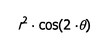 Z6:
 Z8:
 Z9:
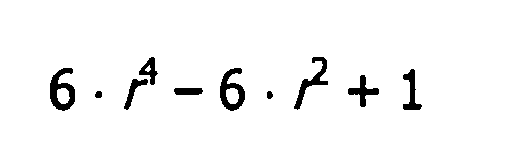 Z12:
 Z13:

- Verfahren nach Anspruch 2, wobei der Schritt des Berechnens folgende Schritte umfasst:Bestimmen der Empfindlichkeiten unterschiedlicher Strukturen in dem Muster auf unterschiedliche Aberrationen;Bestimmen der optimalen Kombination von Aberrationen unter Verwendung der bestimmten Empfindlichkeiten.
- Verfahren nach Anspruch 9, wobei die Empfindlichkeiten bestimmt werden durch Simulieren von Bildern der unterschiedlichen Strukturen mit unterschiedlichen Ausmaßen und/oder Kombinationen von Aberrationen.
- Verfahren nach einem der vorhergehenden Ansprüche, wobei der Absorber eine Dicke größer 50nm aufweist.
- Computer-Verfahren zum Bestimmen von Systemaberrationen, die in einem Projektionssystem einer lithographischen Vorrichtung bewirkt werden sollen, um Abbildungsartefakte zu kompensieren, die durch eine Maske hervorgerufen werden, wobei das Verfahren den Befehl an den Computer umfasst, folgende Schritte durchzuführen:Bestimmen der Empfindlichkeiten unterschiedlicher Strukturen in dem Muster auf unterschiedliche Aberrationen;Bestimmen der optimalen Kombination von Aberrationen unter Verwendung der bestimmten Empfindlichkeiten;dadurch gekennzeichnet, dass die Abbildungsartefakte durch abschattende Effekte eines dicken Absorbers hervorgerufen werden, der ein Muster in einer reflektierenden Maske definiert.
- Verfahren nach Anspruch 12, wobei der Schritt des Bestimmens der Empfindlichkeiten das Simulieren von Bildern der unterschiedlichen Strukturen mit unterschiedlichen Ausmaßen und/oder Kombinationen von Aberrationen umfasst.
- Verfahren nach Anspruch 12 oder 13, wobei der Schritt des Bestimmens der optimalen Kombination von Aberrationen das Bestimmen einer Kombination von Aberrationen umfasst, die bewirkt werden sollen, so dass Werte von wenigstens einer Abbildungsmetrik für unterschiedliche Strukturarten, die in dem Muster erscheinen, näher zusammengebracht werden.
- Verfahren nach Anspruch 14, wobei die wenigstens eine Abbildungsmetrik aus der Gruppe bestehend aus: beste Brennpunktverschiebung, Isofokalneigung, kritische Dimension, Gleichförmigkeit der kritischen Dimension, Überlagerung, Telezentrizität, Musterasymmetrie, Abstandslinearität und isodichte Vorspannung ausgewählt ist.
- Verfahren nach Anspruch 14 oder 15, wobei die unterschiedlichen Strukturen dichte und isolierte Linien und/oder horizontale und vertikale Linien und/oder Linien unterschiedlicher Breite sind.
- Verfahren nach Anspruch 14 oder 15, wobei der Schritt des Bestimmens der optimalen Kombination von Aberrationen das Bestimmen einer Kombination von Aberrationen umfasst, die zu erzielen sind, um Verfahrensfenster für die unterschiedlichen Strukturen näher zusammen zu bringen.
- Verfahren nach einem der vorhergehenden Ansprüche 12 bis 17, wobei die Systemaberrationen Zernike-Polynominale Z2 (Neigung in X), Z3 (Neigung in Y), und Z7 (Koma X) umfasst, wobei diese Polynominale folgende Form annehmen:Z2:
 Z3:
 Z7:
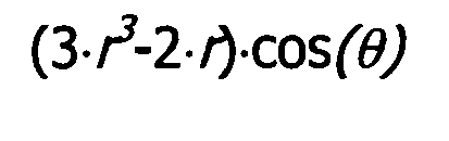
- Computer-Programm, das Code-Einrichtungen umfasst, die bei Ausführung auf einem Computer-System dem Computer-System den Befehl erteilen, die Schritte von einem der Ansprüche 12 bis 18 durchzuführen.
- Computer-Programm, das Code-Einrichtungen umfasst, die bei Ausführung auf einem Computer-System dem Computer-System den Befehl erteilen, eine lithographische Projektionsvorrichtung zu steuern, indem Systemaberrationen in dem Projektionssystem der lithographischen Projektionsvorrichtung durchgeführt werden, um die Abbildung einer Maske zu optimieren, indem Abbildungsartefakte kompensiert werden, die durch die Maske hervorgerufen worden sind,
dadurch gekennzeichnet, dass
die Abbildungsartefakte durch abschattende Effekte eines dicken Absorbers hervorgerufen werden, der ein Muster in einer reflektierenden Maske definiert.
Priority Applications (1)
| Application Number | Priority Date | Filing Date | Title |
|---|---|---|---|
| EP20030257415 EP1434099B1 (de) | 2002-11-28 | 2003-11-25 | Verfahren zur Herstellung einer Vorrichtung |
Applications Claiming Priority (3)
| Application Number | Priority Date | Filing Date | Title |
|---|---|---|---|
| EP02258208 | 2002-11-28 | ||
| EP02258208 | 2002-11-28 | ||
| EP20030257415 EP1434099B1 (de) | 2002-11-28 | 2003-11-25 | Verfahren zur Herstellung einer Vorrichtung |
Publications (2)
| Publication Number | Publication Date |
|---|---|
| EP1434099A1 EP1434099A1 (de) | 2004-06-30 |
| EP1434099B1 true EP1434099B1 (de) | 2008-07-02 |
Family
ID=32471905
Family Applications (1)
| Application Number | Title | Priority Date | Filing Date |
|---|---|---|---|
| EP20030257415 Expired - Lifetime EP1434099B1 (de) | 2002-11-28 | 2003-11-25 | Verfahren zur Herstellung einer Vorrichtung |
Country Status (1)
| Country | Link |
|---|---|
| EP (1) | EP1434099B1 (de) |
Families Citing this family (3)
| Publication number | Priority date | Publication date | Assignee | Title |
|---|---|---|---|---|
| SG124407A1 (en) * | 2005-02-03 | 2006-08-30 | Asml Netherlands Bv | Method of generating a photolithography patterningdevice, computer program, patterning device, meth od of determining the position of a target image on or proximate a substrate, measurement device, and lithographic apparatus |
| ATE467153T1 (de) * | 2005-12-09 | 2010-05-15 | Imec | Verfahren und vorrichtungen zur lithographie |
| CN115437225A (zh) * | 2022-09-21 | 2022-12-06 | 南京诚芯集成电路技术研究院有限公司 | 一种绘制光刻工艺窗口的方法 |
Family Cites Families (5)
| Publication number | Priority date | Publication date | Assignee | Title |
|---|---|---|---|---|
| US6078380A (en) * | 1991-10-08 | 2000-06-20 | Nikon Corporation | Projection exposure apparatus and method involving variation and correction of light intensity distributions, detection and control of imaging characteristics, and control of exposure |
| JP3303436B2 (ja) * | 1993-05-14 | 2002-07-22 | キヤノン株式会社 | 投影露光装置及び半導体素子の製造方法 |
| US6115108A (en) * | 1998-12-04 | 2000-09-05 | Advanced Micro Devices, Inc. | Illumination modification scheme synthesis using lens characterization data |
| EP1251402B1 (de) * | 2001-03-30 | 2007-10-24 | ASML Netherlands B.V. | Lithographischer Apparat und Verfahren zur Herstellung einer Vorrichtung |
| EP1271247A1 (de) * | 2001-06-20 | 2003-01-02 | ASML Netherlands B.V. | Verfahren und Maske für Projektionsbelichtung |
-
2003
- 2003-11-25 EP EP20030257415 patent/EP1434099B1/de not_active Expired - Lifetime
Also Published As
| Publication number | Publication date |
|---|---|
| EP1434099A1 (de) | 2004-06-30 |
Similar Documents
| Publication | Publication Date | Title |
|---|---|---|
| US7042550B2 (en) | Device manufacturing method and computer program | |
| US7580113B2 (en) | Method of reducing a wave front aberration, and computer program product | |
| EP2261739B1 (de) | Verfahren und Apparat zur Erzeugung überlagerter Strukturen auf einem Substrat | |
| US7538952B2 (en) | Lithographic apparatus, aberration correction device and device manufacturing method | |
| US7732110B2 (en) | Method for exposing a substrate and lithographic projection apparatus | |
| JP4787282B2 (ja) | デバイス製造方法、コンピュータプログラム、及び、リソグラフィ装置 | |
| US7374869B2 (en) | Lithographic processing method and device manufactured thereby | |
| US7889316B2 (en) | Method for patterning a radiation beam, patterning device for patterning a radiation beam | |
| US9891532B2 (en) | Lithographic method to apply a pattern to a substrate and lithographic apparatus | |
| US20060057471A1 (en) | Lithographic apparatus and device manufacturing method | |
| US8237914B2 (en) | Process, apparatus, and device for determining intra-field correction to correct overlay errors between overlapping patterns | |
| JP5209755B2 (ja) | リソグラフィ装置およびデバイス製造方法 | |
| US8248579B2 (en) | Lithographic apparatus, device manufacturing method and device for correcting overlay errors between overlapping patterns | |
| WO2018077587A1 (en) | Lithographic apparatus and method | |
| EP1434099A1 (de) | Verfahren zur Herstellung einer Vorrichtung | |
| US20090153821A1 (en) | Lithographic apparatus with adjusted exposure slit shape enabling reduction of focus errors due to substrate topology and device manufacturing method | |
| EP1801657A1 (de) | Herstellungsverfahren für Bauelemente und Computerprogramm | |
| US7663741B2 (en) | Lithographic apparatus, device manufacturing method, calibration method and computer program product | |
| US7148954B2 (en) | Lithographic apparatus and method for its use | |
| EP1471386A1 (de) | Lithographisches Verfahren, sowie damit hergestelltes Gerät | |
| EP1515189A2 (de) | Methode zur Belichtung eines Substrats und lithographischer Projektionsapparat |
Legal Events
| Date | Code | Title | Description |
|---|---|---|---|
| PUAI | Public reference made under article 153(3) epc to a published international application that has entered the european phase |
Free format text: ORIGINAL CODE: 0009012 |
|
| AK | Designated contracting states |
Kind code of ref document: A1 Designated state(s): AT BE BG CH CY CZ DE DK EE ES FI FR GB GR HU IE IT LI LU MC NL PT RO SE SI SK TR |
|
| AX | Request for extension of the european patent |
Extension state: AL LT LV MK |
|
| RAP1 | Party data changed (applicant data changed or rights of an application transferred) |
Owner name: ASML NETHERLANDS B.V. |
|
| 17P | Request for examination filed |
Effective date: 20041209 |
|
| AKX | Designation fees paid |
Designated state(s): DE FR GB IT NL |
|
| 17Q | First examination report despatched |
Effective date: 20050318 |
|
| 17Q | First examination report despatched |
Effective date: 20050318 |
|
| GRAP | Despatch of communication of intention to grant a patent |
Free format text: ORIGINAL CODE: EPIDOSNIGR1 |
|
| GRAS | Grant fee paid |
Free format text: ORIGINAL CODE: EPIDOSNIGR3 |
|
| GRAA | (expected) grant |
Free format text: ORIGINAL CODE: 0009210 |
|
| AK | Designated contracting states |
Kind code of ref document: B1 Designated state(s): DE FR GB IT NL |
|
| REG | Reference to a national code |
Ref country code: GB Ref legal event code: FG4D |
|
| REF | Corresponds to: |
Ref document number: 60321883 Country of ref document: DE Date of ref document: 20080814 Kind code of ref document: P |
|
| PGFP | Annual fee paid to national office [announced via postgrant information from national office to epo] |
Ref country code: NL Payment date: 20081113 Year of fee payment: 6 Ref country code: DE Payment date: 20081121 Year of fee payment: 6 |
|
| PGFP | Annual fee paid to national office [announced via postgrant information from national office to epo] |
Ref country code: IT Payment date: 20081120 Year of fee payment: 6 |
|
| PGFP | Annual fee paid to national office [announced via postgrant information from national office to epo] |
Ref country code: FR Payment date: 20081113 Year of fee payment: 6 |
|
| PLBE | No opposition filed within time limit |
Free format text: ORIGINAL CODE: 0009261 |
|
| STAA | Information on the status of an ep patent application or granted ep patent |
Free format text: STATUS: NO OPPOSITION FILED WITHIN TIME LIMIT |
|
| 26N | No opposition filed |
Effective date: 20090403 |
|
| PGFP | Annual fee paid to national office [announced via postgrant information from national office to epo] |
Ref country code: GB Payment date: 20081117 Year of fee payment: 6 |
|
| REG | Reference to a national code |
Ref country code: NL Ref legal event code: V1 Effective date: 20100601 |
|
| GBPC | Gb: european patent ceased through non-payment of renewal fee |
Effective date: 20091125 |
|
| REG | Reference to a national code |
Ref country code: FR Ref legal event code: ST Effective date: 20100730 |
|
| PG25 | Lapsed in a contracting state [announced via postgrant information from national office to epo] |
Ref country code: NL Free format text: LAPSE BECAUSE OF NON-PAYMENT OF DUE FEES Effective date: 20100601 Ref country code: FR Free format text: LAPSE BECAUSE OF NON-PAYMENT OF DUE FEES Effective date: 20091130 |
|
| PG25 | Lapsed in a contracting state [announced via postgrant information from national office to epo] |
Ref country code: DE Free format text: LAPSE BECAUSE OF NON-PAYMENT OF DUE FEES Effective date: 20100601 |
|
| PG25 | Lapsed in a contracting state [announced via postgrant information from national office to epo] |
Ref country code: GB Free format text: LAPSE BECAUSE OF NON-PAYMENT OF DUE FEES Effective date: 20091125 |
|
| PG25 | Lapsed in a contracting state [announced via postgrant information from national office to epo] |
Ref country code: IT Free format text: LAPSE BECAUSE OF NON-PAYMENT OF DUE FEES Effective date: 20091125 |