EP1434103A2 - Appareil lithographique avec sous-systéme d'alignement, méthode de fabrication d'un dispositif utilisant un alignement, et structure d'alignement - Google Patents
Appareil lithographique avec sous-systéme d'alignement, méthode de fabrication d'un dispositif utilisant un alignement, et structure d'alignement Download PDFInfo
- Publication number
- EP1434103A2 EP1434103A2 EP03079041A EP03079041A EP1434103A2 EP 1434103 A2 EP1434103 A2 EP 1434103A2 EP 03079041 A EP03079041 A EP 03079041A EP 03079041 A EP03079041 A EP 03079041A EP 1434103 A2 EP1434103 A2 EP 1434103A2
- Authority
- EP
- European Patent Office
- Prior art keywords
- alignment structure
- alignment
- phase
- measurement light
- intensity
- Prior art date
- Legal status (The legal status is an assumption and is not a legal conclusion. Google has not performed a legal analysis and makes no representation as to the accuracy of the status listed.)
- Withdrawn
Links
Images


Classifications
-
- G—PHYSICS
- G03—PHOTOGRAPHY; CINEMATOGRAPHY; ANALOGOUS TECHNIQUES USING WAVES OTHER THAN OPTICAL WAVES; ELECTROGRAPHY; HOLOGRAPHY
- G03F—PHOTOMECHANICAL PRODUCTION OF TEXTURED OR PATTERNED SURFACES, e.g. FOR PRINTING, FOR PROCESSING OF SEMICONDUCTOR DEVICES; MATERIALS THEREFOR; ORIGINALS THEREFOR; APPARATUS SPECIALLY ADAPTED THEREFOR
- G03F9/00—Registration or positioning of originals, masks, frames, photographic sheets or textured or patterned surfaces, e.g. automatically
- G03F9/70—Registration or positioning of originals, masks, frames, photographic sheets or textured or patterned surfaces, e.g. automatically for microlithography
- G03F9/7073—Alignment marks and their environment
- G03F9/7076—Mark details, e.g. phase grating mark, temporary mark
-
- G—PHYSICS
- G03—PHOTOGRAPHY; CINEMATOGRAPHY; ANALOGOUS TECHNIQUES USING WAVES OTHER THAN OPTICAL WAVES; ELECTROGRAPHY; HOLOGRAPHY
- G03F—PHOTOMECHANICAL PRODUCTION OF TEXTURED OR PATTERNED SURFACES, e.g. FOR PRINTING, FOR PROCESSING OF SEMICONDUCTOR DEVICES; MATERIALS THEREFOR; ORIGINALS THEREFOR; APPARATUS SPECIALLY ADAPTED THEREFOR
- G03F9/00—Registration or positioning of originals, masks, frames, photographic sheets or textured or patterned surfaces, e.g. automatically
- G03F9/70—Registration or positioning of originals, masks, frames, photographic sheets or textured or patterned surfaces, e.g. automatically for microlithography
- G03F9/7088—Alignment mark detection, e.g. TTR, TTL, off-axis detection, array detector, video detection
Definitions
- the present invention relates in a first aspect to a lithographic apparatus comprising:
- the present invention relates to a device manufacturing method comprising the steps of:
- the present invention relates to an alignment structure for aligning a work piece relative to a reference position using optical measurements, such as interferometric measurements, the alignment structure comprising at least one phase grating mark having a plurality of adjacent lines and spaces with a predetermined periodicity.
- patterning means as here employed should be broadly interpreted as referring to means that can be used to endow an incoming radiation beam with a patterned cross-section, corresponding to a pattern that is to be created in a target portion of the substrate; the term “light valve” can also be used in this context.
- the said pattern will correspond to a particular functional layer in a device being created in the target portion, such as an integrated circuit or other device (see below). Examples of such patterning means include:
- Lithographic apparatus can be used, for example, in the manufacture of integrated circuits (ICs).
- the patterning means may generate a circuit pattern corresponding to an individual layer of the IC, and this pattern can be imaged onto a target portion (e.g. comprising one or more dies) on a substrate (silicon wafer) that has been coated with a layer of radiation-sensitive material (resist).
- a target portion e.g. comprising one or more dies
- a substrate silicon wafer
- a layer of radiation-sensitive material resist
- a single wafer will contain a whole network of adjacent target portions that are successively irradiated via the projection system, one at a time.
- employing patterning by a mask on a mask table a distinction can be made between two different types of machine.
- each target portion is irradiated by exposing the entire mask pattern onto the target portion in one go; such an apparatus is commonly referred to as a wafer stepper or step-and-repeat apparatus.
- a wafer stepper or step-and-repeat apparatus In an alternative apparatus ⁇ commonly referred to as a step-and-scan apparatus ⁇ each target portion is irradiated by progressively scanning the mask pattern under the projection beam in a given reference direction (the "scanning" direction) while synchronously scanning the substrate table parallel or anti-parallel to this direction; since, in general, the projection system will have a magnification factor M (generally ⁇ 1), the speed V at which the substrate table is scanned will be a factor M times that at which the mask table is scanned.
- M magnification factor
- a pattern (e.g. in a mask) is imaged onto a substrate that is at least partially covered by a layer of radiation-sensitive material (resist).
- the substrate Prior to this imaging step, the substrate may undergo various procedures, such as priming, resist coating and a soft bake. After exposure, the substrate may be subjected to other procedures, such as a post-exposure bake (PEB), development, a hard bake and measurement/inspection of the imaged features.
- PEB post-exposure bake
- This array of procedures is used as a basis to pattern an individual layer of a device, e.g. an IC.
- Such a patterned layer may then undergo various processes such as etching, ion-implantation (doping), metallization, oxidation, chemo-mechanical polishing, etc., all intended to finish off an individual layer. If several layers are required, then the whole procedure, or a variant thereof, will have to be repeated for each new layer. Eventually, an array of devices will be present on the substrate (wafer). These devices are then separated from one another by a technique such as dicing or sawing, whence the individual devices can be mounted on a carrier, connected to pins, etc.
- the projection system may hereinafter be referred to as the "lens"; however, this term should be broadly interpreted as encompassing various types of projection system, including refractive optics, reflective optics, and catadioptric systems, for example.
- the projection system may also include components operating according to any of these design types for directing, shaping or controlling the projection beam of radiation, and such components may also be referred to below, collectively or singularly, as a "lens”.
- the lithographic apparatus may be of a type having two or more substrate tables (and/or two or more mask tables). In such "multiple stage” devices the additional tables may be used in parallel, or preparatory steps may be carried out on one or more tables while one or more other tables are being used for exposures. Dual stage lithographic apparatus are described, for example, in US 5,969,441 and WO 98/40791, both incorporated herein by reference.
- the substrate Before a pattern can be projected onto a substrate, the substrate has to be accurately positioned relative to the patterning means, so that the pattern will be projected onto the substrate accurately at a required position. In modem semiconductor manufacturing this positioning has to be realized with nanometer accuracy.
- EP-A-1148390 describes such alignment, using a phase grating alignment system.
- a phase grating alignment system uses a substrate that includes an alignment structure with periodically variable optical properties.
- the phase grating alignment system measures the phase of the period of the alignment structure relative to some reference position that is defined (directly or indirectly) relative to the patterning means. From the phase, a measurement of the position of the substrate is obtained.
- the phase measurement is realised by incorporating the alignment structure in an optical interference arrangement that outputs light with an intensity that depends on the phase.
- the interference arrangement contains for example an imaging element that selects light diffracted by the alignment structure in a selected order of diffraction and images the selected light onto a reference structure in the lithographic apparatus.
- the reference structure has spatially periodically variable optical properties, with a period that corresponds to the period of the image of the alignment structure.
- the light output through the reference structure forms a kind of Moiré pattern.
- This pattern varies as the image of the alignment structure moves relative to the reference structure, dependent on the extent to which the image of the least reflective parts of the periods of the alignment structure coincide with the least transmissive parts of the periods of the reference structure.
- the spatially averaged intensity of the output light varies periodically as a function of the position of the substrate.
- European patent application No. EP 1148390 describes how interference may be used between light from the alignment structure that reaches a detector along two paths which correspond to images of the alignment structure that have been rotated 180 degrees with respect to one another.
- the centre of that rotation serves to provide a defined position relative to the lithographic apparatus and the detected light intensity varies periodically as a function of the position of the substrate relative to the defined position.
- the periodic variation of the averaged intensity can be measured without requiring a detector with high spatial resolution.
- the measurement of the intensity of the detected light makes it possible to assign phase values to different positions of the alignment structure.
- the phase values in turn are used for accurate positioning of the substrate in the direction of periodical variation of the optical properties of the alignment structure.
- phase grating alignment subsystem allows a high alignment accuracy to be realised. Selection of an individual order of diffraction considerably reduces noise since only light which has the spatial frequency of the alignment structure is detected. Compared to alignment techniques that use electronic pattern recognition of images of semiconductor wafers phase grating filtering techniques realise accurate and low-noise alignment with detection and control circuits that are less critical for the alignment.
- the phase grating alignment technique has the problem that it only works when sufficiently large alignment structures and/or reference structures can be used such that the substrate can be initially positioned so that the alignment structure is imaged onto the reference structure. In other words, the capture range of the phase grating alignment must be sufficiently large. Large alignment structures and/or reference structures are expensive, e.g. because they occupy space on the substrate which could otherwise contain circuit components. Therefore it is desirable to reduce the area of the alignment structures and/or the reference structures. However, it has been found that when an alignment structure is less than a given size the structure, although still suitable for accurate positioning purposes, will not always work immediately because the image of the alignment structure has no overlap with the reference structure when the substrate is initially positioned (insufficient capture range).
- the periodic alignment structure in combination with the interference arrangement will provide an output signal with a certain periodicity in it.
- the position can be accurately positioned, but only within 8.0 ⁇ m.
- a periodicity of 88 ⁇ m exists.
- periodicity is defined as the dimension of a single period of a periodic signal.
- the alignment subsystem is further arranged to use a non-periodic feature provided on the alignment structure which is detectable as a capture position or a check position.
- a check position may e.g. be used as a starting point for further alignment or as a confidence check.
- a precise capture point or position for starting a fine wafer alignment can be provided by the present lithography apparatus. This allows removal of the periodic error ambiguity of existing (fine) wafer alignment methods, in any case beyond the periodicity of the fine alignment method.
- the present lithographic apparatus may be used to check afterwards (i.e. after or during alignment of the wafer) whether or not a periodic error has been made.
- the capture range of the alignment subsystem may be extended, and using the alignment subsystem a posteriori as a check will increase the robustness of the alignment subsystem.
- the non-periodic feature is formed by a phase shift between two parts of the alignment structure by a change of the width of one (or more) of the lines or spaces of the alignment structure.
- the alignment structure has two parts with the same periodicity of lines and spaces, but one (or more) of the spaces is reduced or enlarged in length to provide the non-periodic feature.
- One exemplary form reduces the space at the intersection of the two parts to half the periodicity of the phase grating (e.g. 4 ⁇ m in the case of a 8.0 ⁇ m phase grating) or extends it to one and half the periodicity (i.e. 12 ⁇ m for the same phase grating). Effectively, in the transition region, the contributions to the measured signal of the alignment subsystem is then exactly in opposite phase for the two parts, which allows easy detection of the capture position (i.e. the position where the phase gradient of the detected signal is maximum).
- the optical interference arrangement comprises a reference grating
- the non-periodic feature comprises a transition from a first part to a second part of the alignment structure with a first and second periodicity, respectively, which first and second periodicity are below, respectively greater than the periodicity of the reference grating
- the alignment subsystem is arranged to detect the capture position or check position from the resulting sloped phase information of the measurement light.
- periodicity is the dimension of a single period in a periodical system, i.e. the dimension of a combination of a line and a space (greater periodicity thus means that the distance between two consecutive lines is larger).
- the phase of the detected signal will change linearly with varying mutual displacement, but with opposite sign for the first part and second part.
- the capture position or check position can then be derived from the intersection of the two sloped phase signals.
- the resulting phase of the detected signal may in a further embodiment have the form of a sinusoidal shape, which allows an easy detection of the capture position, e.g. using a sinus profile fitting of the detected phase signal.
- the alignment structure comprises a position dependent period change according to in which ⁇ (x) is the position dependent period change, x is the position along the alignment structure and L is the length of the alignment structure over which the phase should vary, and the alignment subsystem is arranged to detect the capture position or check position from the resulting sinusoidal shaped phase information of the measurement light.
- a first embodiment utilizes the finite dimension of the alignment structure as a non-periodic feature.
- the alignment subsystem is arranged to detect the capture position from the envelope of the intensity of the measurement light.
- alignment structures in phase grating alignment systems are longer than they are wide, and the fine wafer alignment is executed using a scan of the alignment structure along its longest direction. To find a capture position for the coarse wafer alignment, the envelope of the detected alignment signal corresponds with the dimensions of the alignment structure used, and thus allows a capture position to be found.
- the alignment structure has a first dimension in a first direction and a second dimension in a second direction, in which the second direction is substantially perpendicular to the first, in which the non-periodic feature is the first and/or second dimension of the alignment structure.
- This first and/or second dimension may be detected using a scan of the alignment mark at an angle ⁇ between 0° and 90° with the first direction.
- This embodiment may be used for all kinds of alignment structures, and is also called diagonal scan.
- the capture position in the second direction may be found.
- alignment is performed in both the first and second direction, using mutually perpendicular alignment structures. So when scanning a first alignment mark (extending in the first direction) a capture position may be derived for the second alignment mark (extending in the second direction) and vice versa.
- the diagonal scan is performed at an angle ⁇ larger than 0°, more preferably at an angle ⁇ larger than 10°, e.g. at an angle ⁇ of 45°.
- This embodiment may also be used when two alignment structures are present on the wafer for the alignment subsystem (e.g. a 8.0 ⁇ m and a 8.8 ⁇ m phase grating). After a diagonal scan is performed at an angle ⁇ to the first direction for the first alignment structure, the scanning is repeated for the second alignment structure, but now at an angle - ⁇ to the first direction. This will provide a capture position with a higher confidence (more robust solution).
- the alignment subsystem e.g. a 8.0 ⁇ m and a 8.8 ⁇ m phase grating
- the scanning is performed along the first direction only. Due to the finite dimension of the alignment structure, also in the first direction, this provides a capture position in the first direction.
- the scanning is performed along the second direction of the alignment structure.
- the dimension of the alignment structure in the second direction is precisely known, this allows to determine a capture position in the second direction, which may be used when performing fine alignment using a second alignment structure.
- the reference grating and the alignment structure are precisely aligned, so that a very small resulting signal is detected. This may be prevented by using a reference grating with a periodicity different from the alignment structure, or by performing a new scan at a slightly offset starting position.
- the non-periodic feature is formed by the transition from a first part of the alignment structure to a second part of the alignment structure, the first part having a periodicity of X ⁇ m and the second part having a periodicity of X/n ⁇ m, n being an integer number.
- the alignment subsystem is arranged to detect the capture position or check position from a change in the intensity of an n-th order of diffraction of the measurement light. Two part alignment structures are relatively easy to produce, especially when choosing the parameters correctly. Care must be taken that the shift in intensity of the detected alignment signal is large enough to be detected reliably, but also that the lower signal still has a sufficiently high amplitude.
- the non-periodic feature is formed by the transition from a first part of the alignment structure to a second part of the alignment structure, the first part having a first duty cycle value of the lines and spaces and the second part having a second duty cycle value of the lines and spaces, and the alignment subsystem is arranged to detect the capture position or check position from a change in the intensity of the measurement light.
- Duty cycle is the ratio of the width of a line and a space in the alignment structure.
- alignment under control of phase information involves a selection step, wherein a position of the substrate is selected so that the alignment structure and the reference structure are in an overlapping imaging relationship.
- the selection step involves determining the amplitude of intensity variations of the measurement light output from the interference arrangement and a search for a position of the substrate so that the alignment structure and the reference structure are in an overlapping imaging relationship.
- intensity measurements are subjected to different processing for the alignment step and for the pre-positioning step respectively.
- the phase of the periodic variations of the intensity is determined, during selection amplitude information of the variations is determined, preferably after filtering out variations that do not match variations due to relative movement of the alignment structure.
- a detector which may be implemented as a suitably programmable computer that processes the same type of intensity information that is also used for phase measurement, but specialized detection hardware may be used as well. Subsequently, the alignment is performed at a position at or near a maximum of the measure of the amplitude.
- the amplitude of the variations as a function of position of the substrate is filtered with a filter that is selective for variations in the amplitude that correspond to the spatial frequency of the period of the alignment pattern and the filtered amplitudes are use in the search.
- One way of implementing filtering is to correlate the amplitude variations with a plurality of mutually displaced versions of a basic matching pattern. Correlation techniques are also often used to determine the phase, but in that case a single displaced version suffices. By using correlation techniques circuitry of a type that is used to determine the phase may also be used to determine the amplitude information.
- a phase grating alignment technique is used for alignment, wherein only selected orders of diffraction from the alignment structure are used to determine the amplitudes.
- the phase of the intensity variation of the measurement light is used for alignment in one direction, typically the direction in which the periods of the alignment structure follow one another.
- further alignment structures on the substrate and/or reference structures in the lithographic apparatus may be used to control alignment in another direction transverse to said direction.
- a single alignment structure and/or reference structure may be used for the two-dimensional search for a position of the substrate for the preposition prior to control dependent on the phase. This is possible because the amplitude of the intensity variations of the output radiation is indicative of overlap in two dimensions even when the phase is indicative of position in only one dimension.
- a similar effect may be caused by the way the alignment structure is imaged onto the reference structure, for example by the shape of pupil apertures used to filter light from selected order of diffraction. Therefore, in an embodiment the maximum is preferably used only to search for the component of the alignment position along a direction transverse to the direction of periodic variation of the alignments structure.
- Different alignment structures may be present in mutually orthogonal scribe lanes areas on a wafer.
- the amplitudes obtained from alignment structures with periodic variations in a first and second mutually transverse directions in different scribe lanes are used to search for different components of the alignment position transverse to the first and second direction respectively.
- alignment structures in horizontal scribe lanes are used for searching for the vertical component of the alignment position and alignment structures in vertical scribe lanes are used for searching for the horizontal component of the alignment position. Because an alignment structure extends over a large range along the length of the scribe-lane the initial position along this length is usually not critical during the search to ensure that the alignment structure is encountered when the apparatus scans transverse to this length direction.
- the alignment structure comprises a non-periodic feature which is detectable as a capture position using the alignment subsystem.
- an alignment structure as defined in the opening paragraph above, in which the alignment structure comprises a non-periodic feature. Further advantageous embodiments are described in the associated dependent claims.
- UV radiation e.g. with a wavelength of 365, 248, 193, 157 or 126 nm
- EUV extreme ultra-violet
- particle beams such as ion beams or electron beams.
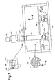
- Figure 1 schematically depicts a lithographic apparatus 1 according to a particular embodiment of the invention.
- the apparatus comprises:
- the apparatus is of a transmissive type (i.e. has a transmissive mask). However, in general, it may also be of a reflective type, for example (with a reflective mask). Alternatively, the apparatus may employ another kind of patterning means, such as a programmable mirror array of a type as referred to above.
- the source LA (e.g. a laser source) produces a beam of radiation.
- This beam is fed into an illumination system (illuminator) IL, either directly or after having traversed conditioning means, such as a beam expander Ex, for example.
- the illuminator IL may comprise adjusting means AM for setting the outer and/or inner radial extent (commonly referred to as ⁇ -outer and ⁇ -inner, respectively) of the intensity distribution in the beam.
- ⁇ -outer and ⁇ -inner commonly referred to as ⁇ -outer and ⁇ -inner, respectively
- it will generally comprise various other components, such as an integrator IN and a condenser CO.
- the beam PB impinging on the mask MA has a desired uniformity and intensity distribution in its cross-section.
- the source LA may be within the housing of the lithographic apparatus (as is often the case when the source LA is a mercury lamp, for example), but that it may also be remote from the lithographic apparatus, the radiation beam which it produces being led into the apparatus (e.g. with the aid of suitable directing mirrors); this latter scenario is often the case when the source LA is an excimer laser.
- the current invention and claims encompass both of these scenarios.
- the mask table MT may just be connected to a short stroke actuator, or may be fixed.
- Mask MA and substrate W may be aligned using mask alignment marks M1, M2 and substrate alignment marks P1, P2.
- the depicted apparatus can be used in two different modes:
- FIG. 1 An alignment subsystem 21 (not shown in figure 1) is included in the apparatus for accurately measuring the position of substrate W to ensure that substrate W is properly aligned during projection.
- Figure 2 schematically shows the alignment subsystem 21, containing an optical subsystem with a radiation source 20, an imaging structure 24, reference structures 26, 26a (forming an optical interference arrangement), detectors 28, 28a and a processing unit 29.
- processing unit 29 is shown as one element, it will be understood that processing unit 29 may be made up of a number of interconnected processors.
- Radiation source 20, for example a laser is arranged to generate a spot of light on an area 22 on substrate W.
- Imaging structure 24 contains a lens arrangement 240, 242 to image area 22 onto reference structure 26.
- Reference structure 26 has spatially periodic transmissive properties.
- Detector 28 is arranged to detect a spatially averaged intensity of radiation transmitted by reference structure 26. Detector 28 has an output coupled to an input of processing unit 29, which in turn has a control output coupled to second positioning means PW, which are coupled to substrate
- Interferometric measuring means IF have an output coupled to processing unit 29. It will be understood that various changes may be made to the alignment subsystem 21 without affecting its function. For example, mirrors may be added to be able to move elements of the alignment subsystem to more convenient locations. In one embodiment the alignment subsystem 21 is immediately next to the projection lens, but it will be understood that the alignment subsystem 21 may be further removed from the projection lens. It is not necessary that the substrate is in the path of the projection beam during alignment. In fact, another substrate, on a separate substrate table may even be in the path of the projection beam during alignment.
- radiation from radiation source 20 is reflected from area 22 and imaging structure 24 uses the reflected radiation to image area 22 onto reference structure 26.
- the imaged radiation is partially transmitted by reference structure 26 onto detector 28 which generates an electric signal that is indicative of the spatially averaged intensity of the transmitted radiation.
- Processing unit 29 uses this electric signal to generate control signals for positioning means PW. This involves a number of stages (which may be executed by different elements (not shown) of processing unit 29).
- a pre-positioning stage processing unit 29 moves substrate W and the alignment subsystem 21 relative to one another so that an alignment structure is imaged onto reference structure 26.
- an accurate positioning stage processing unit 29 accurately measures the position of substrate W and the alignment subsystem 21 relative to one another, i.e. it determines for which output value of interferometric measuring means IF substrate W and alignment subsystem 21 are in a specific alignment relative to one another.
- processing unit 29 uses this measurement to control one or more positions with a predetermined offset to a position at which substrate W and the alignment subsystem 21 are in alignment, to which substrate is moved for illumination with projection beam PB.
- substrate W contains an alignment structure 10 (see figures 3, 5, 7, 9 and 10, to be discussed below) with spatially periodic reflection properties in area 22.
- this alignment structure 10 is imaged onto reference structure 26.
- the spatially averaged amount of light transmitted by reference structure 26 depends periodically on the relative phase of the image of the alignment structure 10 and reference structure 26.
- imaging structure 24 passes only selected pairs of orders of diffraction onto reference structure 26.
- imaging structure 24 has been designed to filter out selected orders of diffraction from area 22.
- imaging element contains lenses 240, 242 with a diffraction order filter 244 in between.
- a first lens 240 maps light diffracted in respective directions to respective positions on diffraction order filter 244, which transmits only light from selected positions.
- a second lens forms an image of area 22 from the transmitted light.
- a number of pairs of diffraction orders of the light from area 22 are treated separately.
- wedges 245 are provided to ensure that different pairs of orders are imaged onto different reference structures 26, 26a, each provided with its own detector 28, 28a.
- the imaging structure 24 is arranged to filter out the 0-th order, effectively halving the period (or doubling the frequency) of the alignment structure 10.
- a 16 ⁇ m period of the alignment structure 10 on the wafer W then effectively becomes a 8 ⁇ m period on the reference grating 26.
- imaging structure 24 may comprise a combination of lenses or imaging mirrors.
- the alignment structure or mark 10 in the area 22 on the wafer W may comprise two different gratings for both the X-and Y-direction (see figure 3).
- two different grating periods for each of the marks 10 e.g. 8.0 and 8.8 ⁇ m
- the capture range is the range in which an alignment can be executed without ambiguities. Because of the periodicity of the gratings, however, there is still an inherent ambiguity in the fine positioning.
- Coarse Wafer Alignment (COWA) followed by a FIWA may be performed in certain embodiments. Also the COWA and FIWA may be executed simultaneously.
- the FIWA may be performed using separate marks 10, such as the known 8.0 ⁇ m phase grating, or the known combination of a 8.0 ⁇ m and 8.8 ⁇ m phase grating using e.g. the above described technique using the Nonius principle.
- the FIWA is performed using the mark 10 according to an embodiment of the present invention (when these include at least a section with the normal period phase grating).
- the present method and use of a phase grating as a mark 10 may be applied to check whether the right initial position has been found to perform a FIWA using a single, e.g. 8.0 ⁇ m, grating mark (confidence check).
- the coarse wafer alignment may be effected using a number of different types of phase gratings for the mark 10.
- the underlying principle of all these types is that a non-periodic feature of the phase grating is used to avoid ambiguities that exist when only using the fine wafer alignment method.
- the capture range and/or the robustness of a periodic alignment system e.g. using 8.0 ⁇ m gratings or a combination of 8.0 ⁇ m and 8.8 ⁇ m gratings
- a periodic alignment system e.g. using 8.0 ⁇ m gratings or a combination of 8.0 ⁇ m and 8.8 ⁇ m gratings
- the non-periodic feature may be included in the phase grating mark 10 on the wafer in a number of manners.
- a number of embodiments of the marks according to the present invention will be discussed below, together with possible specific processing required for that embodiment.
- two classes of marks 10 which embody the present invention exist, i.e. a first class in which the phase of a detected signal is used to determine the mark position (or better: non-periodic feature position), and a second class in which the amplitude of a detected signal is used to determine the mark position.
- phase Jump Mark 10 As a first type of mark 10, a so called Phase Jump Mark is shown in figure 3.
- the reference grating 26 e.g. with a periodicity of 8.0 ⁇ m
- phase jump mark 10 As a first type of mark 10, a so called Phase Jump Mark is shown in figure 3.
- the reference grating 26 e.g. with a periodicity of 8.0 ⁇ m
- Such a phase grating mark 10 comprises lines and spaces as conventional alignment marks (e.g. spaced at 8.0 ⁇ m), but the periodicity of the grating is broken at one or more positions 15 of the mark, resulting in a phase jump of the mark at this position(s).
- the phase jump mark 10 comprises two parts 11, 12 with a phase grating having the same periodicity of lines and spaces, and a feature region 15 between the two parts 11, 12 where the space is not filled with a phase grating having the same periodicity of lines and spaces as the two parts 11, 12.
- a 8.0 ⁇ m phase grating e.g. one of the spaces 15 may be reduced to 4 ⁇ m, 4/7 ⁇ m, 200 nm or enlarged to 12 ⁇ m (the 12 ⁇ m embodiment as shown in figure 3).
- the phase difference between the reference grating and part 11 would differ ⁇ from the phase difference between the reference grating and part 12.
- phase change will occur when the reference grating 26 is moved with respect to the phase grating 10 on the wafer W using the alignment subsystem 21 discussed above.
- This phase change is present in each of the detected orders n of the reflected light beam.
- the signal received on one or more of the detectors 28, 28a may be processed to derive the phase of the received signal, e.g. by applying a best fit on the measured and processed signal phases in a predetermined position window.
- the captured alignment mark position 15 is present.
- the detected signal at the actual alignment position is actually the weakest signal over a larger position window. This of course may result in unreliable results.
- the weak signal is the result of the left and right part of the phase jump mark 10 with a 4 ⁇ m spacing being out of phase.
- the spacing is made much smaller (in the order of 100 nm, e.g. 200 nm) this signal weakening effect is much less prominent or even absent, and still the spacing 15 is large enough to be detected using the phase detection method.
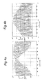
- figure 4a shows the alignment signal S as a function of the displacement x from the alignment subsystem 21 for the phase jump mark having a 4 ⁇ m spacing
- figure 4b shows the alignment signal S as a function of the displacement x from the alignment subsystem 21 for the phase jump mark having a 200 nm spacing. It can be seen, that the alignment signal S for the 200 nm spacing phase jump mark 10 has a much larger signal strength at the aligned position than the alignments signal S for the 4 ⁇ m spacing phase jump mark 10.
- the non-periodic feature of the mark 10 can also be embodied as a linear phase profile mark (LPPM).
- LPPM linear phase profile mark
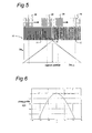
- This embodiment is shown in figure 5.
- two parts 11, 12 of the phase grating 10 both have a period (slightly) different from the reference grating 26.
- two linearly varying phase profile signals can be detected.
- the alignment signal looks like
- the aligned position varies ( ⁇ /8) micron per micron shift of the expected position.
- the gratings 11, 12 of the LPPM 10 are constructed such that the detected alignment phase signal ⁇ x ap shows two slopes with opposite slope sign (See figure 5 bottom part). The unique alignment position can than be derived from the intersection of the two slopes.
- the different periods of the LPPM 10 will lead to different diffraction angles, which must still be transmitted by the diffraction order filter 244 (see figure 2).
- a change in the period of 8 nm will lead to a change in phase slope of 1 nm/ ⁇ m which can be accurately measured.
- a relative period change of 1 ⁇ will lead to a shift of the diffraction order of ⁇ 3 ⁇ m.
- the two slopes may be measured using a single reference grating 26 and a single illumination spot, or, as depicted in figure 5, using two reference gratings 26 and two illumination spots which both move in the direction indicated by the arrow to allow simultaneous determination of the two sloped signals.
- the variation of the grating period has a sinusoidal profile (Sinusoidal Phase Profile Mark, SPPM).
- SPPM Seusoidal Phase Profile Mark
- the two slopes in the resulting measured signal are then replaced by a sinusoidal shape, of which the top can easily be detected.
- the period of the sinusoidal phase profile is much larger than the period of the reference grating (e.g. > 8 ⁇ m, preferably even > 88 ⁇ m)
- a sinus fitting of the detected phase signal profile would provide the capture position 15 of the alignment mark 10.
- Such a sinusoidal phase profile can be obtained from a position-dependent period change: where again we have the boundary condition that ⁇ (x) ⁇ 8.
- ⁇ (x) is the position-dependent period change
- x is the distance along the (longitudinal) x-direction
- L is the alignment mark 10 length.
- An example of the sinusoidal phase profile (solid line), and the associated required position dependent period change ⁇ (x) (broken line) for the SPPM 10 is shown in figure 6.
- the second class of marks 10 uses the intensity of the detected alignment signal to provide the capture position of the non-periodic feature 15 of the mark 10.
- a first embodiment of the second class of marks 10 use is made of the finite properties of regularly used marks, such as a versatile scribeline primary mark (VSPM), a regular 8.0 ⁇ m phase grating mark or a combination of a 8.0 ⁇ m and 8.8 ⁇ m phase mark.
- the marks present are scanned under an angle ⁇ to the longitudinal direction of the mark 10.
- FIG 7 an exemplary arrangement of the scanning with the illumination spot and an existing phase grating mark 10 comprising two separate phase gratings 31, 32 is shown. In this case, both phase gratings 31, 32 present (e.g.
- phase gratings 31 and 32 are scanned by an illumination spot 30 with the same (but opposite signed) scanning angle ⁇ .
- ⁇ scanning angle
- a coordinate axis is shown, indicating that the phase gratings 31 and 32 have their longest dimension in the x-direction and a smaller dimension in the y-axis.
- the intensity signal detected by the alignment subsystem 21 for a single scan (e.g. left part in figure 7, detecting the 8.0 ⁇ m grating 31) is shown in the plot of figure 8 as a function of the y-position.
- the envelope of the detected signal is shown by the broken line, which allows to determine the capture position.
- the detected capture position in this case, however, is the capture position in the direction (y-direction) perpendicular to the longitudinal direction (x-direction) of the phase grating 31.
- the diagonal scan method as discussed with reference to the embodiment shown in figure 7, may also be executed using only a single grating 31.
- phase marks 10 are present on the wafer in both the x- and y-direction in a known configuration (i.e.
- the found capture positions in the x- and y-direction can be used as expected positions in a normal coarse alignment procedure (e.g. using a combination of 8.0 ⁇ m and 8.8 ⁇ m phase gratings as described above).
- a normal coarse alignment procedure e.g. using a combination of 8.0 ⁇ m and 8.8 ⁇ m phase gratings as described above.
- the accuracy of the diagonal scan procedure is e.g.
- This diagonal scan method prevents making a periodic error, as during a scan of a phase grating 31..34, there will only be one distinct envelope shape present in the detected signal.
- no signal or a signal below a predetermined threshold
- the search window of the alignment subsystem 21 should be extended or shifted (e.g. with a positional shift equal to the (known) length of the phase grating 31...34.
- the diagonal scan method is particularly suited to check whether the detected position of the wafer alignment using a detection method having possible periodic errors, is correct (confidence check).
- the non-periodic feature 15 of the mark 10 is the start and end of the phase grating 31...34 in the longitudinal direction of the phase grating 31...34.
- the capture position (either the first edge or the second edge of the phase grating 31...34, or a combination thereof) may be derived from the envelope of the detected alignment signal, the length of which should generally correspond to the length of the phase grating 31...34.
- the non-periodic feature of the phase grating is the start and end of the phase grating 31...34 in the cross direction (i.e. perpendicular to the longitudinal direction).
- a capture position in one direction e.g. y-direction
- the reference grating 26 and the phase grating mark 10 happen to be aligned so that they are exactly out of phase, it is possible that no signal is detected at all using the alignment subsystem 21. This can also happen when the angle is very near to 90° and the lines are less wide than the spaces.
- the diagonal scan method of the alignment subsystem provides a number of further advantages, which are predominantly present for the cases in which 0° ⁇ ⁇ ⁇ 90°.
- the scan doesn't necessarily use more time than conventional scans, as the signal acquisition for capturing and aligning can be performed simultaneously. Also, no further hardware needs to be added to the alignment subsystem 21, as the illuminating beam (spot 30) and associated drive means, and the detectors 28 and associated processing elements 29 are already present.
- the diagonal scan uses the same marks 10 on the wafer W as used for the fine wafer alignment, no further space is needed in the scribelanes on the wafer W.
- the robustness of the diagonal scan method is the same as for the existing fine wafer alignment: when a phase grating mark 10 can be detected using the normal (x-direction) scanning of a phase grating mark 10, the phase grating mark 10 will also be detected using the diagonal scanning method.
- the choice of the size of the illuminating beam is a trade off: for optimal performance it should be very small to prevent cross talk with other features on the wafer W.
- a very small illuminating beam will enlarge the chance of missing the phase grating mark 10 at all.
- the chance of actually hitting the phase grating mark 10 (which is much longer than wide) is greatly enhanced, allowing to actually use a small illuminating beam.
- X 8.0 ⁇ m
- n an integer number
- Duty cycle is the ratio of the width of a line and a space in the alignment structure.
- phase gratings 10 are provided with lines and spaces of equal dimension (duty cycle 50%). When the duty cycle of the lines and spaces is changed, this will be noticeable in the amplitude of the signal from the alignment subsystem 21, and this will indicate the capture position 15 of this embodiment of the mark 10.
- FIG 11 shows a flow chart of part of the operation of processing unit 29.
- the flow-chart contains a prepositioning stage 301, an alignment measurement stage 302 and a positioning-during-projection stage 303.
- the prepositioning stage contains a number of steps.
- the steps of the flow chart are implemented for example by providing a suitable program of instructions in an instruction memory (not shown) of processing unit 29 for execution by a conventional computer (not shown) in processing unit 29.
- Prepositioning stage 301 contains a first, second and third step 304, 305, 316.
- processing unit 29 causes to measure signals from detector 28 (and optionally from detector 28a and further detectors) at a series of positions of substrate W.
- first step 304 includes a first sub-step 311 of moving the substrate or wafer W to a series of positions relative to the measuring subsystem and a second sub-step 312 in which an intensity signal from detector 28 is measured at these positions. The range of these positions is substantially larger than the size of reference structure 26 (and the illumination beam 30).
- a third sub-step 313 ensures that the first and second sub-step are repeated for different positions.
- Figure 12 shows a top view of part of a substrate W with an alignment structure 40.
- a scanning path 42 has been indicated.
- Path 42 is not part of substrate W, but indicates successive locations 44 of substrate W at which radiation source 20 provides spots of light on substrate W which are imaged onto reference structure 26, during sub-step 311.
- the apparatus is arranged to scan along a meandering path of lines. This provides for a two dimensional search area with minimal movement.
- Window 46 indicates the size of an area of points on substrate W that are imaged onto reference structure 26 at a single time. As can be seen the image of alignment structure 40 will overlap with reference structure 26 only for a limited number of positions along scanning path 42 as indicated by the line (path 42) crossing the alignment structure 40.
- processing unit 29 computes amplitude information for a number of positions along scanning path 42.
- second step 305 contains a first sub-step 314 in which the intensity amplitude information is computed.
- a second sub-step 315 ensures that the first sub-step is repeated for a number of positions.
- Figure 13 shows an output signal of detector 28 as a function of position (in micrometers) along a horizontal part of scanning path 42 along substrate W as a continuous curve (although in practice measurements of the output may be performed only at certain sampling positions).
- positions around 500 micrometer
- the output signal varies periodically as a function of position.
- a more or less random variation of smaller amplitude occurs due to structures present in substrate W that are not alignment structures, such as circuit structures in the case of a semi-conducting manufacturing process.
- the more or less random variations involve amplitude and phase variations of a sine wave with a period corresponding to the selected orders of diffraction.
- processing unit 29 computes amplitude information of the variations of the output signal for a number of positions (with coordinates x,y on substrate W as measured by interferometric measuring means IF) along scanning path 42.
- the computation of the amplitude information involves determining a measure of the amplitude of the variations of the output signal. For substrates W that do not produce much output signal in the absence of the alignment structure it suffices to detect the amplitude, for example by taking the difference between minima and maxima (at different positions), or by measuring the maximum deviation from the average output signal value. For other substrates W a certain amount of spatial filtering is preferred that suppresses the amplitudes of output signal variations that do not have the spatial frequency expected for the alignment structure. This may be realized for example by band pass filtering the output signal prior to amplitude measurement, or by correlation techniques that are selectively sensitive for the expected output signal from alignment structure 40.
- the sum is over locations with coordinates x', y', including at least a series of locations with different x' coordinate values spaced less than the width of alignment structure from one another.
- A2(x,y) is the amplitude information A2 for a location with coordinates x,y as determined from the output s(x',y) of detector 28 with substrate positioned at a locations with coordinates x',y'.
- the parameter k is equal to 2 ⁇ /p, where p is the period of the image of the alignment structure 40 onto reference structure 26, 26a.
- the range of coordinates x',y' extends over a window that extends around the position with the coordinates x,y for which the amplitude information is computed. The size of the window can be selected freely. A larger range ensures larger frequency selectivity, making false detection of alignment structures less likely, but reduces position accuracy and vice versa.
- the range of x',y' values that contributes to the sums is taken to have approximately the same size as alignment structure
- processing unit 29 uses the computed amplitude information to select a position (x0,y0) where the computed amplitude information is maximal as a function of a and y.
- a formula for A2 has been given by way of example it should be appreciated without deviating from the inventions other types of formula may be used.
- a formula for the derivative of A2 with respect to x may be computed to locate the maximum, or a product with a weighting functions W(x-x', x-y') included in the sums, W decreasing as x'and/or y' move away from x,y may be.
- measurements from a detector 28 for a single pair of diffraction orders suffice to find the maximum.
- similar determinations of amplitudes for different pairs of diffraction orders may be used, either to compute a combined amplitude function or to confirm whether a maximum occurs for all pairs of orders of diffraction prior to using the location of the maximum.
- Alignment measuring stage 302 is comparable to prepositioning stage 301, except that instead of an amplitude a phase is determined. Moreover, in alignment measuring stage 302 measurements are made preferably only at positions where the alignment structure is at a position from which it images onto reference structure 26.
- processing unit 29 executes a first sub-step 321 similar to first and second sub-steps 311, 312 of prepositioning stage 301, involving moving to a number of locations and measuring output signals of detector 28 for different positions of substrate W.
- a second sub-step 322 ensures repetition at a number of different locations relative to the alignment subsystem: These number of different locations, have coordinates (x",y0) that are selected dependent on the position (x0,y0) produced in fourth step 316, with coordinates (x",y0) wherein x" is varied over a range around x0.
- the sum is over a range of locations with different x" which preferably extends over a range that is equal to the size of alignment structure 40, different x" values preferably being spaced by less than a period of reference structure 26.
- Choice of the y" values do not appreciably affect the computation, as long as they are within the size of the alignment structure, preferably a range of y" values is used in the sum.
- phase value provides accurate position information of alignment structure 40 relative to the alignment sub-system.
- In positioning-during-projection stage 303 of the flow-chart processing unit 29 uses this information to position substrate W at a series of required positions relative to the patterning means.
- the determination of the phase is performed for a number of pairs of orders of diffraction and a combination of the computed phases is used to determine the position of the alignment structure.
- xr may be used.
- a weight function W(x"-x0,y"-y0) may be used in the sums, or the some recursive process may be used to adjust x0 until "b" becomes zero, in which xr coincides with the adjusted x0.
- phase ⁇ and the amplitude A2 use the same type of elements: summing cosine functions and sine functions. Nevertheless the formulas lead to two different types of information.
- the phase value ⁇ varies linearly substantially in the same way as a function of position x0, no matter how wide the range of positions (x",y") over which the sums are taken.
- the amplitude information A2 in contrast increases in strength as this range increased, be it with an accompanying decrease in position dependence. This makes the amplitude information suitable for searching among areas that do not contain the alignment structure and the phase information suitable for accurate positioning once it is known where the alignment structure 40 is located.
- the use of similar elements makes it possible to use much of processing unit 29 for both computations.
- reference position xr from phase value ⁇ is ambiguous, in the sense that any value of xr that differs by a integer multiple of the period p could be determined. Under some circumstances the prepositioning accuracy may be sufficient to identify a single xr value as the correct value, but generally this is not the case. Therefore one or more additional spatially periodic alignment structures are preferably provided on substrate W at predetermined relative positions with respect to alignment structure 40. The period or periods of this additional alignments structure or structures differ from the period of alignment structure 40.
- the alignment sub-system is preferably provided with additional reference structures, detectors etc. to determine the phase of the intensity variations due to displacement of the substrate relative to the alignment sub-system.
- Phase values determined in this way make it possible to increase the distance between ambiguous xr values up to a point that the prepositioning accuracy suffices to select the correct xr value.
- the additional alignment structures may be measured using the same reference structure. This allows to predict the differences in aligned positions coming from the different alignment structures based on a model and a priori information on the shape and relative positions of the additional alignment structures and the first alignment structure.
- the phase ⁇ only provides information about the position of the alignment structure in a direction along which the optical properties of alignment structure 40 vary periodically. Therefore one or more further alignment structures, reference structures etc. are preferably provided with periodical spatial variation in a direction transverse to the period of alignment structure 40 (preferably perpendicular). These one or more further alignment structures are preferably provided at predetermined positions relative to alignment structure 40. During alignment stage 302 these one or more further alignment structures are used to obtain additional phase values for accurately positioning substrate W in the direction transverse to the direction perpendicular to the period of alignment structure 40.
- Processing unit 29 preferably uses the position (x0,y0) selected in third step 316 to control the positions of substrate W where the phase value of the additional alignment structure or structures and the one or more further alignment structures is determined, using amplitude information obtained by using at least one of the alignment structure, the additional alignment structures and the further alignment structures.
- Using a single one of the alignment structures for pre-positioning simplifies processing and is usually sufficiently accurate, both in a direction perpendicular to the period of that alignment structure and in directions transverse thereto. But when increased pre-positioning accuracy is required a combined amplitude value for different alignment structures may be used, for example by summing amplitude information obtained for different alignment structures, taking account of the predetermined offset of these structures on substrate W.
- Figure 14 depicts a further top view of part of a substrate W.
- substrate W way is a semi-conductor substrate on which areas for different integrated circuit chips are reserved. Between the areas for the integrated circuit chips scribe-lanes 78 are provided which will be sacrificed when substrate W is mechanically split into different integrated circuit chips.
- Periodic alignment structures 70, 72 are present in the scribe-lanes 78. For the sake of clarity only two periodic alignment structures 70, 72 are shown, but it should be understood that more will generally be present.
- the optical properties of the alignment structures 70, 72 vary periodically along the direction in which scribe-lanes 78 run, i.e. in the horizontal direction for horizontal scribe lanes between rows of integrated circuit chips and in the vertical direction for vertical scribe lanes between columns of integrated circuit chips.
- the extent of a periodic alignment structure 70, 72 transverse to the direction of the scribe lane in which it is incorporated is relatively narrow compared with its extent along that direction.
- Scanning paths 74, 76 run transverse to the direction in which the optical properties of periodic alignment structures 70, 72 vary periodically.
- the amplitude of the periodic variation of the intensity of the measured light for a particular alignment structure is determined as a function of position along the scanning path 74, 76 transverse to the direction in which the optical properties of periodic alignment structures 70, 72 vary periodically (non-scan direction).
- the intensity of the measurement light for each position along the scanning path 74, 76 is measured at a number of different positions in the direction in which the optical properties of periodic alignment structures 70, 72 vary periodically (scan direction).
- the position transverse to the direction of the scanning path is determined where the amplitude shows best overlap of mark and reference structure.
- this is a position where a maximum amplitude occurs, but in case of a trapezoid shape of the maximum any position in a region with level maximum amplitude as a function of position may be used.. This is done for periodic alignment structures 70, 72 in two mutually transverse scribe lanes.
- the results are used to control respective components of the position where the phase will be measured to realize accurate alignment. That is, the position of the maximum along the scanning path 74 transverse to the alignment structure 70 with optical properties that vary periodically in the horizontal direction is used to determine the vertical position component of alignment structure 72 for accurate alignment, and the position of the maximum along the scanning path 76 transverse to the alignment structure 72 with optical properties that vary periodically in the vertical direction is used to determine the horizontal position component of alignment structure 72 for accurate alignment.
- an accurate position can thus be determined. More generally, when the image of the alignment structure is narrow an accurate position is realized in this way (a narrow image may be a result of a narrow alignment structure, but also of imaging, for example of a form of filtering of orders of diffraction that passes a wider bandwidth transverse to the direction of periodic variation). Moreover, when the alignment structures generally extend over a relatively large extent transverse to the scanning path, pre-positioning is usually sufficiently accurate so that the apparatus needs to try only one transverse scanning line for one alignment structure
- a plurality of measurement intensities for each position along the scanning path 70, 72 is measured at a number of different positions in the direction in which the optical properties of periodic alignment structures 70, 72 vary periodically.
- a meandering scanning path may be used which extends far less in the direction of periodic variation than in the transverse direction, or a series of short scans along the direction of periodic variation at a number of positions in the transverse directions.
- the maximum is preferably determined for at least two parallel scanning paths that are a quarter of a period (plus any number of full periods) apart. But any other distance unequal to an integer number of half periods may be used. As described, alignment is performed in a number of distinct stages and steps.
- the decomposition into stages and steps merely serves to facilitate explanation of the alignment process.
- the various stages and steps need not be distinct.
- the phase be determined from stored intensity measurements that have been obtained before, after or concurrently with (or are indeed part of) the measurements that are obtained at a series of relative positions of the substrate and the alignment measuring system for determining the position of maximum amplitude.
- the determination of the location of maximum amplitude merely serves to select which of the stored intensity measurements should be used.
- separate intensity measurements performed at locations selected under control of the location of maximum amplitude may be used for determining the phase. This requires less storage space for measurements, but it increases the time needed for alignment, since substrate W has to be moved to the selected locations.
- a suitably programmed computer or set of computers for the determination of phase and amplitude, as well as the search for the relative position of substrate and alignment measuring system that leads to maximum amplitude
- dedicated (not or only partly programmable) elements may be used to perform any one or a combination of these operations.
- a digital signal processing circuit may be used to perform the filter operations that filter out intensity variations of the expected frequency and to compute the phase and amplitude.
- specialized hardware amplitude detection circuitry may be used, such as used for AM radio demodulation may be coupled to detector 28.
- Figure 15 shows an alternative alignment system.
- reference structure 26 has been omitted.
- a rotating element 60 has been added, which combines light diffracted in orders of diffraction with mutually opposite sign n, -n rotating the image of the alignment structure of the opposite orders over 180 degrees relative to one another, e.g. rotating one over 90 degrees and the other over -90 degrees.
- n mutually opposite sign
- -n rotating the image of the alignment structure of the opposite orders over 180 degrees relative to one another, e.g. rotating one over 90 degrees and the other over -90 degrees.
- the intensity of the combined light is measured at a detector 28. In this case no reference structure is needed in front of detector 28.
- the output of detector 28 may be used in the way described for figure 2.
Landscapes
- Physics & Mathematics (AREA)
- General Physics & Mathematics (AREA)
- Engineering & Computer Science (AREA)
- Multimedia (AREA)
- Exposure Of Semiconductors, Excluding Electron Or Ion Beam Exposure (AREA)
- Container, Conveyance, Adherence, Positioning, Of Wafer (AREA)
- Exposure And Positioning Against Photoresist Photosensitive Materials (AREA)
Priority Applications (1)
| Application Number | Priority Date | Filing Date | Title |
|---|---|---|---|
| EP03079041A EP1434103A3 (fr) | 2002-12-16 | 2003-12-12 | Appareil lithographique avec sous-système d'alignement, méthode de fabrication d'un dispositif utilisant un alignement et structure d'alignement |
Applications Claiming Priority (7)
| Application Number | Priority Date | Filing Date | Title |
|---|---|---|---|
| EP02080334 | 2002-12-16 | ||
| EP02080334A EP1431832A1 (fr) | 2002-12-16 | 2002-12-16 | Appareil lithographique et méthode de fabrication d'un dispositif |
| EP03075432 | 2003-02-14 | ||
| EP03075432 | 2003-02-14 | ||
| EP03076010 | 2003-04-04 | ||
| EP03076010 | 2003-04-04 | ||
| EP03079041A EP1434103A3 (fr) | 2002-12-16 | 2003-12-12 | Appareil lithographique avec sous-système d'alignement, méthode de fabrication d'un dispositif utilisant un alignement et structure d'alignement |
Publications (2)
| Publication Number | Publication Date |
|---|---|
| EP1434103A2 true EP1434103A2 (fr) | 2004-06-30 |
| EP1434103A3 EP1434103A3 (fr) | 2009-04-15 |
Family
ID=32475505
Family Applications (1)
| Application Number | Title | Priority Date | Filing Date |
|---|---|---|---|
| EP03079041A Withdrawn EP1434103A3 (fr) | 2002-12-16 | 2003-12-12 | Appareil lithographique avec sous-système d'alignement, méthode de fabrication d'un dispositif utilisant un alignement et structure d'alignement |
Country Status (1)
| Country | Link |
|---|---|
| EP (1) | EP1434103A3 (fr) |
Cited By (11)
| Publication number | Priority date | Publication date | Assignee | Title |
|---|---|---|---|---|
| US7440079B2 (en) | 2004-09-22 | 2008-10-21 | Asml Netherlands B.V. | Lithographic apparatus, alignment system, and device manufacturing method |
| US8006484B2 (en) | 2005-02-14 | 2011-08-30 | Eaton Corporation | Systems and methods for reducing emissions of internal combustion engines using a fuel processor bypass |
| NL2008679A (en) * | 2011-04-22 | 2012-10-23 | Mapper Lithography Ip Bv | Position determination in a lithography system using a substrate having a partially reflective position mark. |
| US9201315B2 (en) | 2011-04-22 | 2015-12-01 | Mapper Lithography Ip B.V. | Lithography system for processing a target, such as a wafer, a method for operating a lithography system for processing a target, such as a wafer and a substrate for use in such a lithography system |
| US9383662B2 (en) | 2011-05-13 | 2016-07-05 | Mapper Lithography Ip B.V. | Lithography system for processing at least a part of a target |
| US9484188B2 (en) | 2015-03-11 | 2016-11-01 | Mapper Lithography Ip B.V. | Individual beam pattern placement verification in multiple beam lithography |
| CN111722480A (zh) * | 2019-03-19 | 2020-09-29 | 东芝存储器株式会社 | 基板处理装置 |
| US11347152B2 (en) | 2018-01-17 | 2022-05-31 | Asml Netherlands B.V. | Scan signal characterization diagnostics |
| US11442372B2 (en) * | 2019-03-27 | 2022-09-13 | Asml Netherlands B.V. | Method of measuring an alignment mark or an alignment mark assembly, alignment system, and lithographic tool |
| WO2023147642A1 (fr) * | 2022-02-01 | 2023-08-10 | Huawei Technologies Canada Co., Ltd. | Systèmes et procédés pour filtrer des longueurs d'onde optiques |
| CN116931393A (zh) * | 2023-08-02 | 2023-10-24 | 上海图双精密装备有限公司 | 光刻设备的对准运动台和光轴z轴垂直度校准方法、装置、设备及存储介质 |
Family Cites Families (2)
| Publication number | Priority date | Publication date | Assignee | Title |
|---|---|---|---|---|
| JP3570728B2 (ja) * | 1997-03-07 | 2004-09-29 | アーエスエム リソグラフィ ベスローテン フェンノートシャップ | 離軸整列ユニットを持つリトグラフ投射装置 |
| US6628406B1 (en) * | 2000-04-20 | 2003-09-30 | Justin L. Kreuzer | Self referencing mark independent alignment sensor |
-
2003
- 2003-12-12 EP EP03079041A patent/EP1434103A3/fr not_active Withdrawn
Cited By (16)
| Publication number | Priority date | Publication date | Assignee | Title |
|---|---|---|---|---|
| US7440079B2 (en) | 2004-09-22 | 2008-10-21 | Asml Netherlands B.V. | Lithographic apparatus, alignment system, and device manufacturing method |
| US8006484B2 (en) | 2005-02-14 | 2011-08-30 | Eaton Corporation | Systems and methods for reducing emissions of internal combustion engines using a fuel processor bypass |
| US9395636B2 (en) | 2011-04-22 | 2016-07-19 | Mapper Lithography Ip B.V. | Lithography system for processing a target, such as a wafer, and a method for operating a lithography system for processing a target, such as a wafer |
| WO2012144904A3 (fr) * | 2011-04-22 | 2013-07-25 | Mapper Lithography Ip B.V. | Détermination d'une position dans un système de lithographie à l'aide d'un substrat doté d'un repère partiellement réfléchissant |
| NL2010979A (en) * | 2011-04-22 | 2013-08-01 | Mapper Lithography Ip Bv | Position determination in a lithography system using a substrate having a partially reflective position mark. |
| US9201315B2 (en) | 2011-04-22 | 2015-12-01 | Mapper Lithography Ip B.V. | Lithography system for processing a target, such as a wafer, a method for operating a lithography system for processing a target, such as a wafer and a substrate for use in such a lithography system |
| US9395635B2 (en) | 2011-04-22 | 2016-07-19 | Mapper Lithography Ip B.V. | Position determination in a lithography system using a substrate having a partially reflective position mark |
| NL2008679A (en) * | 2011-04-22 | 2012-10-23 | Mapper Lithography Ip Bv | Position determination in a lithography system using a substrate having a partially reflective position mark. |
| US9383662B2 (en) | 2011-05-13 | 2016-07-05 | Mapper Lithography Ip B.V. | Lithography system for processing at least a part of a target |
| US9484188B2 (en) | 2015-03-11 | 2016-11-01 | Mapper Lithography Ip B.V. | Individual beam pattern placement verification in multiple beam lithography |
| US11347152B2 (en) | 2018-01-17 | 2022-05-31 | Asml Netherlands B.V. | Scan signal characterization diagnostics |
| CN111722480A (zh) * | 2019-03-19 | 2020-09-29 | 东芝存储器株式会社 | 基板处理装置 |
| CN111722480B (zh) * | 2019-03-19 | 2023-04-14 | 铠侠股份有限公司 | 基板处理装置 |
| US11442372B2 (en) * | 2019-03-27 | 2022-09-13 | Asml Netherlands B.V. | Method of measuring an alignment mark or an alignment mark assembly, alignment system, and lithographic tool |
| WO2023147642A1 (fr) * | 2022-02-01 | 2023-08-10 | Huawei Technologies Canada Co., Ltd. | Systèmes et procédés pour filtrer des longueurs d'onde optiques |
| CN116931393A (zh) * | 2023-08-02 | 2023-10-24 | 上海图双精密装备有限公司 | 光刻设备的对准运动台和光轴z轴垂直度校准方法、装置、设备及存储介质 |
Also Published As
| Publication number | Publication date |
|---|---|
| EP1434103A3 (fr) | 2009-04-15 |
Similar Documents
| Publication | Publication Date | Title |
|---|---|---|
| US7002667B2 (en) | Lithographic apparatus with alignment subsystem, device manufacturing method, and device manufactured thereby | |
| US8208121B2 (en) | Alignment mark and a method of aligning a substrate comprising such an alignment mark | |
| US7440079B2 (en) | Lithographic apparatus, alignment system, and device manufacturing method | |
| US8208140B2 (en) | Alignment system and alignment marks for use therewith | |
| US9606442B2 (en) | Position measuring apparatus, position measuring method, lithographic apparatus and device manufacturing method | |
| CN101458464B (zh) | 对准方法、对准系统以及具有对准标记的产品 | |
| JP4701209B2 (ja) | 角度分解したスペクトロスコピーリソグラフィの特性解析方法および装置 | |
| US8319940B2 (en) | Position measurement system and lithographic apparatus | |
| US20070222960A1 (en) | Lithographic apparatus and device manufacturing method with reduced scribe lane usage for substrate measurement | |
| US20120008126A1 (en) | Lithographic apparatus with multiple alignment arrangements and alignment measuring method | |
| EP1434103A2 (fr) | Appareil lithographique avec sous-systéme d'alignement, méthode de fabrication d'un dispositif utilisant un alignement, et structure d'alignement | |
| JP5357219B2 (ja) | リソグラフィ装置、コンピュータプログラムプロダクト及びデバイス製造方法 | |
| US7349101B2 (en) | Lithographic apparatus, overlay detector, device manufacturing method, and device manufactured thereby | |
| US20030227604A1 (en) | Lithographic apparatus, alignment method and device manufacturing method | |
| US9506743B2 (en) | Position measuring apparatus, position measuring method, lithographic apparatus and device manufacturing method | |
| EP1431832A1 (fr) | Appareil lithographique et méthode de fabrication d'un dispositif | |
| EP1526408A1 (fr) | Appareil lithographique et procédé de fabrication d'un dispositif, et un système de mesure | |
| EP1338924B1 (fr) | Méthode d'alignement et méthode pour la fabrication d'un dispositif | |
| EP1398670A2 (fr) | Procédé d'alignement d'un substrat, programme informatique et procédé pour la production d'un dispositif |
Legal Events
| Date | Code | Title | Description |
|---|---|---|---|
| PUAI | Public reference made under article 153(3) epc to a published international application that has entered the european phase |
Free format text: ORIGINAL CODE: 0009012 |
|
| AK | Designated contracting states |
Kind code of ref document: A2 Designated state(s): AT BE BG CH CY CZ DE DK EE ES FI FR GB GR HU IE IT LI LU MC NL PT RO SE SI SK TR |
|
| AX | Request for extension of the european patent |
Extension state: AL LT LV MK |
|
| RAP1 | Party data changed (applicant data changed or rights of an application transferred) |
Owner name: ASML NETHERLANDS B.V. |
|
| PUAL | Search report despatched |
Free format text: ORIGINAL CODE: 0009013 |
|
| AK | Designated contracting states |
Kind code of ref document: A3 Designated state(s): AT BE BG CH CY CZ DE DK EE ES FI FR GB GR HU IE IT LI LU MC NL PT RO SE SI SK TR |
|
| AX | Request for extension of the european patent |
Extension state: AL LT LV MK |
|
| STAA | Information on the status of an ep patent application or granted ep patent |
Free format text: STATUS: THE APPLICATION IS DEEMED TO BE WITHDRAWN |
|
| AKX | Designation fees paid |
Designated state(s): DE FR GB IT NL |
|
| 18D | Application deemed to be withdrawn |
Effective date: 20090701 |