EP1434272A1 - Herstellungsverfahren für ein halbleiterbauelement - Google Patents
Herstellungsverfahren für ein halbleiterbauelement Download PDFInfo
- Publication number
- EP1434272A1 EP1434272A1 EP02777783A EP02777783A EP1434272A1 EP 1434272 A1 EP1434272 A1 EP 1434272A1 EP 02777783 A EP02777783 A EP 02777783A EP 02777783 A EP02777783 A EP 02777783A EP 1434272 A1 EP1434272 A1 EP 1434272A1
- Authority
- EP
- European Patent Office
- Prior art keywords
- semiconductor device
- film
- manufacturing
- gate insulation
- silicon oxide
- Prior art date
- Legal status (The legal status is an assumption and is not a legal conclusion. Google has not performed a legal analysis and makes no representation as to the accuracy of the status listed.)
- Granted
Links
Images

Classifications
-
- H—ELECTRICITY
- H10—SEMICONDUCTOR DEVICES; ELECTRIC SOLID-STATE DEVICES NOT OTHERWISE PROVIDED FOR
- H10D—INORGANIC ELECTRIC SEMICONDUCTOR DEVICES
- H10D12/00—Bipolar devices controlled by the field effect, e.g. insulated-gate bipolar transistors [IGBT]
- H10D12/01—Manufacture or treatment
- H10D12/031—Manufacture or treatment of IGBTs
-
- H—ELECTRICITY
- H10—SEMICONDUCTOR DEVICES; ELECTRIC SOLID-STATE DEVICES NOT OTHERWISE PROVIDED FOR
- H10D—INORGANIC ELECTRIC SEMICONDUCTOR DEVICES
- H10D30/00—Field-effect transistors [FET]
- H10D30/01—Manufacture or treatment
- H10D30/021—Manufacture or treatment of FETs having insulated gates [IGFET]
- H10D30/028—Manufacture or treatment of FETs having insulated gates [IGFET] of double-diffused metal oxide semiconductor [DMOS] FETs
- H10D30/0291—Manufacture or treatment of FETs having insulated gates [IGFET] of double-diffused metal oxide semiconductor [DMOS] FETs of vertical DMOS [VDMOS] FETs
-
- H—ELECTRICITY
- H10—SEMICONDUCTOR DEVICES; ELECTRIC SOLID-STATE DEVICES NOT OTHERWISE PROVIDED FOR
- H10D—INORGANIC ELECTRIC SEMICONDUCTOR DEVICES
- H10D62/00—Semiconductor bodies, or regions thereof, of devices having potential barriers
- H10D62/80—Semiconductor bodies, or regions thereof, of devices having potential barriers characterised by the materials
- H10D62/83—Semiconductor bodies, or regions thereof, of devices having potential barriers characterised by the materials being Group IV materials, e.g. B-doped Si or undoped Ge
- H10D62/832—Semiconductor bodies, or regions thereof, of devices having potential barriers characterised by the materials being Group IV materials, e.g. B-doped Si or undoped Ge being Group IV materials comprising two or more elements, e.g. SiGe
- H10D62/8325—Silicon carbide
-
- H—ELECTRICITY
- H10—SEMICONDUCTOR DEVICES; ELECTRIC SOLID-STATE DEVICES NOT OTHERWISE PROVIDED FOR
- H10D—INORGANIC ELECTRIC SEMICONDUCTOR DEVICES
- H10D64/00—Electrodes of devices having potential barriers
- H10D64/01—Manufacture or treatment
- H10D64/013—Manufacture or treatment of electrodes having a conductor capacitively coupled to a semiconductor by an insulator
- H10D64/01366—Manufacture or treatment of electrodes having a conductor capacitively coupled to a semiconductor by an insulator the semiconductor being silicon carbide
Definitions
- the present invention relates to a method of manufacturing a field-effect transistor, a bipolar transistor, a thyristor or other such semiconductor device having a metal-insulation film (or oxide film)-semiconductor structure that uses a silicon carbide substrate.
- Silicon carbide is a semiconductor material having excellent characteristics, such as a large band gap, high thermal conductivity, high electron saturation drift velocity and high dielectric breakdown voltage, and is drawing attention as a material for next-generation low-loss power device elements.
- thermal oxidation can be used to form an oxide film from silicon carbide, making a field-effect transistor having a metal-oxide film-semiconductor structure (MOSFET) a leading candidate for silicon carbide power device elements.
- MOSFET metal-oxide film-semiconductor structure
- JP-A HEI 11-31691 discloses a method in which the flow rate of hydrogen is increased to more than the flow ratio of 1:1 between hydrogen and oxygen.
- the embodiments thereof describe using this method to form a gate oxide film, decreasing the interface state density in a MOS capacitor using P-type silicon carbide.
- U.S. Patent No. 5,972,801 discloses using the thermal oxidation method to form a gate oxide film in a range of 1050°C to 1100°C, and following this by heat treatment at 600°C to 1000°C in an atmosphere containing H 2 O.
- oxygen is passed through pure water heated to 95°C (subjected to bubbling) to produce an atmosphere containing H 2 O.
- a conventional MIS- or MOS-type FET that uses a silicon carbide substrate has a channel mobility that is much lower than the electron mobility of bulk silicon carbide, the intrinsic properties of silicon carbide are not reflected in the device characteristics. That is, the FET On resistance (R on ) is much higher than the value that is theoretically predicted based on the property values of silicon carbide.
- silicon carbide having the crystalline structure known as 4H (4H-SiC) has a bulk electron mobility in the order of 900 cm 2 /Vs
- the channel mobility of a MOSFET formed by the usual thermal oxidation method is a very low 5 to 10 cm 2 /Vs.
- Reference 1 K. Ueno et al., Mat. Sci. and Eng.
- the present invention was proposed to resolve the above problem, and has as its object to provide a method of manufacturing MIS- and MOS-type semiconductor devices with high channel mobility that use a silicon carbide substrate.
- the present invention provides a method of manufacturing a semiconductor device that includes a process of forming a gate insulation film on a silicon carbide substrate, further comprising a process of heat treatment for a given time at a temperature of 900°C to 1000°C in an atmosphere containing at least 25% H 2 O (water), after formation of the gate insulation film on the silicon carbide substrate.
- the given heat treatment time in the atmosphere containing H 2 O is from 1 to 5 hours.
- the gate insulation film is silicon oxide film, silicon nitride film or silicon oxide nitride film, or a multilayer film that includes one of these films.
- the gate insulation film is a film formed by a thermal oxidation method or a deposition method, or by a method that is a combination of those methods.
- the thermal oxidation method uses an atmosphere of dry oxygen.
- the atmosphere containing H 2 O (water) further contains one or both of O 2 (oxygen) gas and an inert gas.
- the H 2 O (water) contained in the atmosphere containing H 2 O (water) is produced by thermal reaction of H 2 (hydrogen) gas and O 2 (oxygen) gas.
- the method of manufacturing a semiconductor device according to the present invention further comprises a group of processes that are conducted after the heat treatment process in the atmosphere containing H 2 O and that adopt a maximum temperature of 800°C.
- the silicon carbide substrate has a (000-1) plane orientation.
- the channel mobility of the semiconductor device thus manufactured can be substantially improved by heat treatment at a temperature of 900°C to 1000°C in an atmosphere containing H 2 O after the gate insulation film has been formed on the silicon carbide semiconductor substrate, as described above.
- this invention comprises following the process of forming the gate insulation film on the silicon carbide substrate with heat treatment in an atmosphere containing H 2 O in order to improve the channel mobility of the manufactured FET.
- the above heat treatment in an atmosphere containing H 2 O is carried out after formation of the gate insulation film.
- the effect of the heat treatment also depends on gate insulation film formation conditions (temperature, atmosphere and so forth), and if the conditions are different, there may be cases in which no improvement in channel mobility is seen.
- the heat treatment of the present invention in addition to the moisture concentration of the atmosphere containing H 2 O, there are clear ranges at which conditions relating to heat treatment temperature and heat treatment time are optimal, and improvement in channel mobility may not be seen in cases where there is deviation from these conditions. This behavior is different from that discussed with reference to interface state density in the prior art.
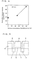
- Figure 5 shows an example of a MOS-type FET using a silicon carbide substrate, manufactured in accordance with the invention.
- a source region 2 and a drain region 3 are provided in a silicon carbide substrate 1 as spaced by a channel region from each other.
- a gate insulation film 5 is provided on the channel region, and a gate electrode 8 is provided on the gate insulation film 5.
- the source region 2 is electrically connected to a source electrode 6 and the drain region 3 is electrically connected to a drain electrode 7, and the source electrode 6, drain electrode 7 and gate electrode are each insulated by an insulation film 4.
- the silicon carbide substrate 1 there were used two types of substrate: a P-type 4H-SiC (0001) epitaxial substrate (having a difference of approximately 5 x 10 15 cm -3 between acceptor density Na and donor density), and a P-type 6H-SiC (0001) epitaxial substrate (having a difference of approximately 5 x 10 15 cm -3 between acceptor density Na and donor density).
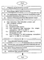
- temperatures were raised and lowered at ⁇ 5°C/minute. Specific details of the processes of manufacturing the MOS-type FETs will now be described, in the order shown in Figure 1.
- Typical respective process conditions pertaining to the following processes are shown below, which processes are gate insulation layer formation 1, annealing 2 in inert gas and heat treatment 3 in H 2 O-containing atmosphere.
- Figure 2 is a diagram showing the gate voltage dependency of the field-effect channel mobility of a MOSFET manufactured by the method of above-described example.
- curve (a) is the channel mobility of a MOSFET (MOSFET (a)) fabricated using a 4H-SiC (0001) substrate
- curve (b) is the channel mobility of a MOSFET (MOSFET (b)) fabricated using a 6H-SiC (0001) substrate.
- the channel mobility of MOSFET (a) was approximately 50 cm 2 /Vs and the channel mobility of MOSFET (b) was approximately 95 cm 2 /Vs.
- the decrease from the maximum channel mobility value ⁇ FEmax to the high gate voltage side (25 V) was small, being in the order of 20%.
- the maximum value ⁇ FEmax in the case of a gate insulation film formed by the usual thermal oxidation method is 5 to 10 cm 2 /Vs in the case of a MOSFET with a 4H-SiC (0001) substrate, and 35 cm 2 /Vs in the case of a MOSFET with a 6H-SiC (0001) substrate, from which it can be seen that with both MOSFETs (a) and (b) manufactured by the method of this invention, major increases in channel mobility ⁇ FE were achieved.
- FIG 3 is a diagram showing the heat-treatment moisture concentration dependency of the maximum field-effect channel mobility of a MOSFET manufactured using a 4H-SiC (0001) substrate.
- the solid bullets ( ⁇ ) are plot points representing the maximum MOSFET channel mobility value ⁇ FEmax at a moisture concentration in the heat-treatment atmosphere of 0% (corresponding to annealing in a dry oxygen atmosphere), 13%, 25%, and 50%.
- the maximum ⁇ FEmax value of the fabricated MOSFETs increases with the increase in the moisture concentration, with the increase in the maximum ⁇ FEmax value being particularly pronounced in the case of MOSFETs fabricated in an atmosphere having a moisture concentration of 25% or more.
- the channel mobilities of MOSFETs fabricated in the above process using heat treatment for 180 minutes at 850°C ( ⁇ ) or 1050°C ( ⁇ ) in an atmosphere containing 25% H 2 O, and MOSFETs thus fabricated using heat treatment for 60 minutes at 950°C in an atmosphere containing 25% H 2 O( ⁇ ) are shown.
- the maximum channel mobility was low, being in the order of 8 cm 2 /Vs.
- Such maximum channel mobility is substantially the same as that obtained using a gate insulation film formed using just the ordinary thermal oxidation.
- the solid bullets ( ⁇ ) are plot points representing the maximum channel mobility value ⁇ FEmax of a MOSFET using a 6H-SiC (0001) substrate fabricated at a moisture concentration in the heat-treatment atmosphere of 25% and 50%.
- the solid squares ( ⁇ ) in the figure denote the values of a MOSFET not subjected to heat treatment in an H 2 O-containing atmosphere after formation of the gate insulation film by thermal oxidation. From the figure, it can be seen that even in the case of a MOSFET that uses a 6H-SiC (0001) substrate, compared to the maximum channel mobility of a MOSFET that uses a gate oxide film formed by ordinary thermal oxidation, an increase in the moisture concentration of the atmosphere is accompanied by a major increase in mobility.
- the channel mobility was approximately 97 cm 2 /Vs in the case of a MOSFET manufactured using an atmosphere having a moisture concentration of 50%.
- the processes after the heat treatment in an H 2 O-containing atmosphere does not include a process at or above a temperature of 800°C, and as a result, fabrication of the semiconductor device can be completed in a state in which the increase in channel mobility resulting from the heat treatment in an H 2 O-containing atmosphere is maintained.
- the processes following the heat treatment in the H 2 O-containing atmosphere included a process at or above the heat treatment temperature, it was confirmed that the effect was reduced.
- channel mobility decreased from 95 cm 2 /Vs to around 70 cm 2 /Vs.
- the effect is not completely extinguished.
- a MIS- or MOS-type semiconductor device having high channel mobility can be realized by, after forming the gate insulation film, using heat treatment for a given time in a water-containing atmosphere.
- channel mobility can be improved by using heat treatment at a temperature of 900°C to 1000°C in an atmosphere containing H 2 O (water) after forming a gate insulation film composed of a single or multiple layers of silicon oxide film, silicon nitride film or silicon oxide nitride film used in a transistor or the like on a silicon carbide region.
- H 2 O water
Landscapes
- Formation Of Insulating Films (AREA)
- Insulated Gate Type Field-Effect Transistor (AREA)
Applications Claiming Priority (3)
| Application Number | Priority Date | Filing Date | Title |
|---|---|---|---|
| JP2001274073A JP2003086792A (ja) | 2001-09-10 | 2001-09-10 | 半導体装置の作製法 |
| JP2001274073 | 2001-09-10 | ||
| PCT/JP2002/009219 WO2003023864A1 (en) | 2001-09-10 | 2002-09-10 | Production method for semiconductor device |
Publications (3)
| Publication Number | Publication Date |
|---|---|
| EP1434272A1 true EP1434272A1 (de) | 2004-06-30 |
| EP1434272A4 EP1434272A4 (de) | 2009-07-01 |
| EP1434272B1 EP1434272B1 (de) | 2011-06-15 |
Family
ID=19099184
Family Applications (1)
| Application Number | Title | Priority Date | Filing Date |
|---|---|---|---|
| EP02777783A Expired - Lifetime EP1434272B1 (de) | 2001-09-10 | 2002-09-10 | Herstellungsverfahren für ein halbleiterbauelement |
Country Status (4)
| Country | Link |
|---|---|
| US (1) | US7256082B2 (de) |
| EP (1) | EP1434272B1 (de) |
| JP (1) | JP2003086792A (de) |
| WO (1) | WO2003023864A1 (de) |
Cited By (7)
| Publication number | Priority date | Publication date | Assignee | Title |
|---|---|---|---|---|
| DE10392870B4 (de) * | 2002-06-28 | 2009-07-30 | National Institute Of Advanced Industrial Science And Technology | Verfahren zur Herstellung einer Halbleitervorrichtung und Halbleitervorrichtung |
| EP1965430A3 (de) * | 2007-02-28 | 2009-08-12 | Denso Corporation | SIC-Halbleiterbauelement und Verfahren zu seiner Herstellung |
| US7880173B2 (en) | 2002-06-28 | 2011-02-01 | National Institute Of Advanced Industrial Science And Technology | Semiconductor device and method of manufacturing same |
| DE102005036063B4 (de) * | 2005-08-01 | 2011-12-01 | New Japan Radio Co. Ltd. | Verfahren zur Herstellung einer Siliziumkarbidhalbleitervorrichtung |
| EP2546867A4 (de) * | 2010-03-12 | 2014-07-09 | Sumitomo Electric Industries | Siliciumcarbid-halbleitervorrichtung und herstellungsverfahren dafür |
| EP2835819A3 (de) * | 2010-06-16 | 2015-07-01 | Sumitomo Electric Industries, Ltd. | Herstellungsverfahren für Siliciumcarbidhalbleitervorrichtung |
| EP3021353A4 (de) * | 2013-07-11 | 2017-02-15 | Fuji Electric Co., Ltd. | Silicium-carbid-halbleiterbauelement und verfahren zur herstellung eines silicium-carbid-halbleiterbauelements |
Families Citing this family (19)
| Publication number | Priority date | Publication date | Assignee | Title |
|---|---|---|---|---|
| JP2005047753A (ja) * | 2003-07-29 | 2005-02-24 | Tadahiro Omi | 炭化珪素製品、その製造方法、及び、炭化珪素製品の洗浄方法 |
| JP2005277253A (ja) * | 2004-03-26 | 2005-10-06 | National Institute Of Advanced Industrial & Technology | 半導体装置の作製方法及び水素処理装置 |
| US7713883B2 (en) * | 2005-03-08 | 2010-05-11 | Hitachi Kokusai Electric Inc. | Manufacturing method of a semiconductor device, and substrate processing apparatus |
| JP2006269641A (ja) * | 2005-03-23 | 2006-10-05 | National Institute Of Advanced Industrial & Technology | 半導体装置及びその製造方法 |
| US7727904B2 (en) | 2005-09-16 | 2010-06-01 | Cree, Inc. | Methods of forming SiC MOSFETs with high inversion layer mobility |
| US7883949B2 (en) * | 2006-06-29 | 2011-02-08 | Cree, Inc | Methods of forming silicon carbide switching devices including P-type channels |
| EP2631951B1 (de) * | 2006-08-17 | 2017-10-11 | Cree, Inc. | Bipolare Hochleistungstransistoren mit isoliertem Gatter |
| JP2008244456A (ja) * | 2007-02-28 | 2008-10-09 | Denso Corp | 炭化珪素半導体装置およびその製造方法 |
| JP4823952B2 (ja) * | 2007-03-26 | 2011-11-24 | 三菱電機株式会社 | 半導体装置の製造方法 |
| JP5157843B2 (ja) * | 2007-12-04 | 2013-03-06 | 住友電気工業株式会社 | 炭化ケイ素半導体装置およびその製造方法 |
| JP5197474B2 (ja) * | 2009-04-17 | 2013-05-15 | 三菱電機株式会社 | 炭化珪素半導体装置の製造方法 |
| JP5659152B2 (ja) | 2009-04-30 | 2015-01-28 | ライオン株式会社 | 半導体用基板の洗浄方法および酸性溶液 |
| JP5610492B2 (ja) | 2009-12-16 | 2014-10-22 | 国立大学法人 奈良先端科学技術大学院大学 | SiC半導体素子およびその作製方法 |
| JP5975460B2 (ja) * | 2012-01-31 | 2016-08-23 | 国立研究開発法人産業技術総合研究所 | 炭化ケイ素半導体装置の製造方法 |
| US20140021464A1 (en) * | 2012-07-17 | 2014-01-23 | National Chung Cheng University | Yttrium-doped Indium Oxide Transparent Conductive Thin-Film Transistor and Method for Making Same |
| JP6331634B2 (ja) * | 2014-04-17 | 2018-05-30 | 住友電気工業株式会社 | 炭化珪素半導体装置の製造方法 |
| CN104637801A (zh) * | 2015-01-30 | 2015-05-20 | 株洲南车时代电气股份有限公司 | 一种制备SiC MOSFET栅氧化层的方法 |
| CN104658903A (zh) * | 2015-01-30 | 2015-05-27 | 株洲南车时代电气股份有限公司 | 一种制备SiC MOSFET栅氧化层的方法 |
| JP2018113371A (ja) | 2017-01-12 | 2018-07-19 | 株式会社ニューフレアテクノロジー | 荷電粒子ビーム描画装置および荷電粒子ビーム描画方法 |
Family Cites Families (10)
| Publication number | Priority date | Publication date | Assignee | Title |
|---|---|---|---|---|
| US5972801A (en) | 1995-11-08 | 1999-10-26 | Cree Research, Inc. | Process for reducing defects in oxide layers on silicon carbide |
| US6028012A (en) * | 1996-12-04 | 2000-02-22 | Yale University | Process for forming a gate-quality insulating layer on a silicon carbide substrate |
| JP3491050B2 (ja) | 1997-05-14 | 2004-01-26 | 富士電機ホールディングス株式会社 | 炭化けい素半導体装置の熱酸化膜形成方法 |
| US5952100A (en) * | 1997-05-21 | 1999-09-14 | General Electric Company | Silicon-doped boron nitride coated fibers in silicon melt infiltrated composites |
| DE19829309B4 (de) * | 1997-07-04 | 2008-02-07 | Fuji Electric Co., Ltd., Kawasaki | Verfahren zur Herstellung eines thermischen Oxidfilms auf Siliciumcarbid |
| JP3085272B2 (ja) * | 1997-12-19 | 2000-09-04 | 富士電機株式会社 | 炭化けい素半導体装置の熱酸化膜形成方法 |
| JP3551909B2 (ja) * | 1999-11-18 | 2004-08-11 | 株式会社デンソー | 炭化珪素半導体装置の製造方法 |
| US6905920B2 (en) * | 2000-09-04 | 2005-06-14 | Seiko Epson Corporation | Method for fabrication of field-effect transistor to reduce defects at MOS interfaces formed at low temperature |
| JP3940560B2 (ja) * | 2001-01-25 | 2007-07-04 | 独立行政法人産業技術総合研究所 | 半導体装置の製造方法 |
| JP4525958B2 (ja) * | 2001-08-27 | 2010-08-18 | 独立行政法人産業技術総合研究所 | 半導体装置の製造方法 |
-
2001
- 2001-09-10 JP JP2001274073A patent/JP2003086792A/ja active Pending
-
2002
- 2002-09-10 US US10/488,243 patent/US7256082B2/en not_active Expired - Lifetime
- 2002-09-10 WO PCT/JP2002/009219 patent/WO2003023864A1/ja not_active Ceased
- 2002-09-10 EP EP02777783A patent/EP1434272B1/de not_active Expired - Lifetime
Cited By (11)
| Publication number | Priority date | Publication date | Assignee | Title |
|---|---|---|---|---|
| DE10392870B4 (de) * | 2002-06-28 | 2009-07-30 | National Institute Of Advanced Industrial Science And Technology | Verfahren zur Herstellung einer Halbleitervorrichtung und Halbleitervorrichtung |
| US7880173B2 (en) | 2002-06-28 | 2011-02-01 | National Institute Of Advanced Industrial Science And Technology | Semiconductor device and method of manufacturing same |
| DE10394372B4 (de) * | 2002-06-28 | 2011-07-28 | National Institute Of Advanced Industrial Science And Technology | Verfahren zur Herstellung einer Halbleitervorrichtung |
| DE102005036063B4 (de) * | 2005-08-01 | 2011-12-01 | New Japan Radio Co. Ltd. | Verfahren zur Herstellung einer Siliziumkarbidhalbleitervorrichtung |
| EP1965430A3 (de) * | 2007-02-28 | 2009-08-12 | Denso Corporation | SIC-Halbleiterbauelement und Verfahren zu seiner Herstellung |
| EP2546867A4 (de) * | 2010-03-12 | 2014-07-09 | Sumitomo Electric Industries | Siliciumcarbid-halbleitervorrichtung und herstellungsverfahren dafür |
| US9012335B2 (en) | 2010-03-12 | 2015-04-21 | Sumitomo Electric Industries, Ltd. | Silicon carbide semiconductor device and method for manufacturing the same |
| EP3223300A1 (de) * | 2010-03-12 | 2017-09-27 | Sumitomo Electric Industries, Ltd. | Siliciumcarbid-halbleiterbauelement und verfahren zur herstellung davon |
| EP2835819A3 (de) * | 2010-06-16 | 2015-07-01 | Sumitomo Electric Industries, Ltd. | Herstellungsverfahren für Siliciumcarbidhalbleitervorrichtung |
| EP3021353A4 (de) * | 2013-07-11 | 2017-02-15 | Fuji Electric Co., Ltd. | Silicium-carbid-halbleiterbauelement und verfahren zur herstellung eines silicium-carbid-halbleiterbauelements |
| US9922822B2 (en) | 2013-07-11 | 2018-03-20 | Fuji Electric Co., Ltd. | Silicon carbide semiconductor device and manufacturing method of silicon carbide semiconductor device |
Also Published As
| Publication number | Publication date |
|---|---|
| US20040242022A1 (en) | 2004-12-02 |
| EP1434272A4 (de) | 2009-07-01 |
| WO2003023864A1 (en) | 2003-03-20 |
| EP1434272B1 (de) | 2011-06-15 |
| JP2003086792A (ja) | 2003-03-20 |
| US7256082B2 (en) | 2007-08-14 |
Similar Documents
| Publication | Publication Date | Title |
|---|---|---|
| US7256082B2 (en) | Production method for semiconductor device | |
| JP4374437B2 (ja) | 半導体装置の製造方法 | |
| US7811874B2 (en) | Method for manufacturing silicon carbide semiconductor device, and silicon carbide semiconductor device | |
| US7880173B2 (en) | Semiconductor device and method of manufacturing same | |
| US7265388B2 (en) | Semiconductor device | |
| JP4525958B2 (ja) | 半導体装置の製造方法 | |
| US6767843B2 (en) | Method of N2O growth of an oxide layer on a silicon carbide layer | |
| US8536066B2 (en) | Methods of forming SiC MOSFETs with high inversion layer mobility | |
| US7538352B2 (en) | Semiconductor device and power converter, driving inverter, general-purpose inverter and high-power high-frequency communication device using same | |
| JP4549167B2 (ja) | 炭化珪素半導体装置の製造方法 | |
| JP2002261275A (ja) | Mosデバイス | |
| CN101635313A (zh) | 碳化硅半导体装置 | |
| KR102324000B1 (ko) | 실리콘 탄화물 반도체 디바이스 및 그 제조 방법 | |
| JP2009016530A (ja) | 炭化珪素電界効果型トランジスタ及びその製造方法 | |
| KR20090048572A (ko) | 탄화규소 반도체 장치 및 그 제조 방법 | |
| JP2003243653A (ja) | 炭化珪素半導体装置の製造方法 | |
| JP5110445B2 (ja) | 半導体装置 | |
| JP2008117878A (ja) | 半導体装置の製造方法 | |
| JP3952978B2 (ja) | 炭化珪素半導体素子 | |
| JP5072482B2 (ja) | 炭化珪素半導体装置の製造方法 | |
| JP2004311815A (ja) | 半導体装置およびその製造方法 | |
| JP2021086896A (ja) | 絶縁ゲート型半導体装置及び絶縁ゲート型半導体装置の製造方法 | |
| JP2007180577A (ja) | 炭化珪素半導体素子 | |
| KR20080033351A (ko) | 반도체 장치의 제조 방법 | |
| JPWO2004090969A1 (ja) | 炭化珪素半導体装置およびその製造方法 |
Legal Events
| Date | Code | Title | Description |
|---|---|---|---|
| PUAI | Public reference made under article 153(3) epc to a published international application that has entered the european phase |
Free format text: ORIGINAL CODE: 0009012 |
|
| 17P | Request for examination filed |
Effective date: 20040323 |
|
| AK | Designated contracting states |
Kind code of ref document: A1 Designated state(s): AT BE BG CH CY CZ DE DK EE ES FI FR GB GR IE IT LI LU MC NL PT SE SK TR |
|
| AX | Request for extension of the european patent |
Extension state: AL LT LV MK RO SI |
|
| A4 | Supplementary search report drawn up and despatched |
Effective date: 20090603 |
|
| RIC1 | Information provided on ipc code assigned before grant |
Ipc: H01L 21/28 20060101AFI20090527BHEP |
|
| 17Q | First examination report despatched |
Effective date: 20100720 |
|
| GRAP | Despatch of communication of intention to grant a patent |
Free format text: ORIGINAL CODE: EPIDOSNIGR1 |
|
| GRAS | Grant fee paid |
Free format text: ORIGINAL CODE: EPIDOSNIGR3 |
|
| GRAA | (expected) grant |
Free format text: ORIGINAL CODE: 0009210 |
|
| AK | Designated contracting states |
Kind code of ref document: B1 Designated state(s): DE GB |
|
| REG | Reference to a national code |
Ref country code: GB Ref legal event code: FG4D |
|
| REG | Reference to a national code |
Ref country code: DE Ref legal event code: R096 Ref document number: 60240297 Country of ref document: DE Effective date: 20110721 |
|
| PLBE | No opposition filed within time limit |
Free format text: ORIGINAL CODE: 0009261 |
|
| STAA | Information on the status of an ep patent application or granted ep patent |
Free format text: STATUS: NO OPPOSITION FILED WITHIN TIME LIMIT |
|
| 26N | No opposition filed |
Effective date: 20120316 |
|
| REG | Reference to a national code |
Ref country code: DE Ref legal event code: R097 Ref document number: 60240297 Country of ref document: DE Effective date: 20120316 |
|
| REG | Reference to a national code |
Ref country code: DE Ref legal event code: R082 Ref document number: 60240297 Country of ref document: DE Representative=s name: BOCKHORNI & KOLLEGEN PATENT- UND RECHTSANWAELT, DE Ref country code: DE Ref legal event code: R082 Ref document number: 60240297 Country of ref document: DE Representative=s name: HEYER, VOLKER, DIPL.-PHYS. DR.RER.NAT., DE |
|
| REG | Reference to a national code |
Ref country code: DE Ref legal event code: R082 Ref document number: 60240297 Country of ref document: DE Representative=s name: HEYER, VOLKER, DIPL.-PHYS. DR.RER.NAT., DE |
|
| PGFP | Annual fee paid to national office [announced via postgrant information from national office to epo] |
Ref country code: GB Payment date: 20210930 Year of fee payment: 20 |
|
| PGFP | Annual fee paid to national office [announced via postgrant information from national office to epo] |
Ref country code: DE Payment date: 20211129 Year of fee payment: 20 |
|
| REG | Reference to a national code |
Ref country code: DE Ref legal event code: R071 Ref document number: 60240297 Country of ref document: DE |
|
| REG | Reference to a national code |
Ref country code: GB Ref legal event code: PE20 Expiry date: 20220909 |
|
| PG25 | Lapsed in a contracting state [announced via postgrant information from national office to epo] |
Ref country code: GB Free format text: LAPSE BECAUSE OF EXPIRATION OF PROTECTION Effective date: 20220909 |