EP1434474A2 - Technique pour interconnecter électriquement des signaux électriques entre un composant électronique et un dispositif d'acheminement de signaux multicouche - Google Patents
Technique pour interconnecter électriquement des signaux électriques entre un composant électronique et un dispositif d'acheminement de signaux multicouche Download PDFInfo
- Publication number
- EP1434474A2 EP1434474A2 EP03394086A EP03394086A EP1434474A2 EP 1434474 A2 EP1434474 A2 EP 1434474A2 EP 03394086 A EP03394086 A EP 03394086A EP 03394086 A EP03394086 A EP 03394086A EP 1434474 A2 EP1434474 A2 EP 1434474A2
- Authority
- EP
- European Patent Office
- Prior art keywords
- electrically conductive
- conductive contacts
- routing device
- signal routing
- array
- Prior art date
- Legal status (The legal status is an assumption and is not a legal conclusion. Google has not performed a legal analysis and makes no representation as to the accuracy of the status listed.)
- Withdrawn
Links
Images





Classifications
-
- H—ELECTRICITY
- H05—ELECTRIC TECHNIQUES NOT OTHERWISE PROVIDED FOR
- H05K—PRINTED CIRCUITS; CASINGS OR CONSTRUCTIONAL DETAILS OF ELECTRIC APPARATUS; MANUFACTURE OF ASSEMBLAGES OF ELECTRICAL COMPONENTS
- H05K1/00—Printed circuits
- H05K1/02—Details
- H05K1/11—Printed elements for providing electric connections to or between printed circuits
-
- H—ELECTRICITY
- H05—ELECTRIC TECHNIQUES NOT OTHERWISE PROVIDED FOR
- H05K—PRINTED CIRCUITS; CASINGS OR CONSTRUCTIONAL DETAILS OF ELECTRIC APPARATUS; MANUFACTURE OF ASSEMBLAGES OF ELECTRICAL COMPONENTS
- H05K1/00—Printed circuits
- H05K1/02—Details
- H05K1/11—Printed elements for providing electric connections to or between printed circuits
- H05K1/115—Via connections; Lands around holes or via connections
-
- H—ELECTRICITY
- H05—ELECTRIC TECHNIQUES NOT OTHERWISE PROVIDED FOR
- H05K—PRINTED CIRCUITS; CASINGS OR CONSTRUCTIONAL DETAILS OF ELECTRIC APPARATUS; MANUFACTURE OF ASSEMBLAGES OF ELECTRICAL COMPONENTS
- H05K1/00—Printed circuits
- H05K1/02—Details
- H05K1/11—Printed elements for providing electric connections to or between printed circuits
- H05K1/111—Pads for surface mounting, e.g. lay-out
- H05K1/112—Pads for surface mounting, e.g. lay-out directly combined with via connections
-
- H—ELECTRICITY
- H05—ELECTRIC TECHNIQUES NOT OTHERWISE PROVIDED FOR
- H05K—PRINTED CIRCUITS; CASINGS OR CONSTRUCTIONAL DETAILS OF ELECTRIC APPARATUS; MANUFACTURE OF ASSEMBLAGES OF ELECTRICAL COMPONENTS
- H05K1/00—Printed circuits
- H05K1/02—Details
- H05K1/0296—Conductive pattern lay-out details not covered by sub groups H05K1/02 - H05K1/0295
- H05K1/0298—Multilayer circuits
-
- H—ELECTRICITY
- H05—ELECTRIC TECHNIQUES NOT OTHERWISE PROVIDED FOR
- H05K—PRINTED CIRCUITS; CASINGS OR CONSTRUCTIONAL DETAILS OF ELECTRIC APPARATUS; MANUFACTURE OF ASSEMBLAGES OF ELECTRICAL COMPONENTS
- H05K2201/00—Indexing scheme relating to printed circuits covered by H05K1/00
- H05K2201/09—Shape and layout
- H05K2201/09209—Shape and layout details of conductors
- H05K2201/09218—Conductive traces
- H05K2201/09227—Layout details of a plurality of traces, e.g. escape layout for Ball Grid Array [BGA] mounting
-
- H—ELECTRICITY
- H05—ELECTRIC TECHNIQUES NOT OTHERWISE PROVIDED FOR
- H05K—PRINTED CIRCUITS; CASINGS OR CONSTRUCTIONAL DETAILS OF ELECTRIC APPARATUS; MANUFACTURE OF ASSEMBLAGES OF ELECTRICAL COMPONENTS
- H05K2201/00—Indexing scheme relating to printed circuits covered by H05K1/00
- H05K2201/09—Shape and layout
- H05K2201/09209—Shape and layout details of conductors
- H05K2201/095—Conductive through-holes or vias
- H05K2201/09509—Blind vias, i.e. vias having one side closed
-
- H—ELECTRICITY
- H05—ELECTRIC TECHNIQUES NOT OTHERWISE PROVIDED FOR
- H05K—PRINTED CIRCUITS; CASINGS OR CONSTRUCTIONAL DETAILS OF ELECTRIC APPARATUS; MANUFACTURE OF ASSEMBLAGES OF ELECTRICAL COMPONENTS
- H05K2201/00—Indexing scheme relating to printed circuits covered by H05K1/00
- H05K2201/09—Shape and layout
- H05K2201/09209—Shape and layout details of conductors
- H05K2201/095—Conductive through-holes or vias
- H05K2201/09536—Buried plated through-holes, i.e. plated through-holes formed in a core before lamination
-
- H—ELECTRICITY
- H05—ELECTRIC TECHNIQUES NOT OTHERWISE PROVIDED FOR
- H05K—PRINTED CIRCUITS; CASINGS OR CONSTRUCTIONAL DETAILS OF ELECTRIC APPARATUS; MANUFACTURE OF ASSEMBLAGES OF ELECTRICAL COMPONENTS
- H05K2201/00—Indexing scheme relating to printed circuits covered by H05K1/00
- H05K2201/09—Shape and layout
- H05K2201/09209—Shape and layout details of conductors
- H05K2201/095—Conductive through-holes or vias
- H05K2201/09627—Special connections between adjacent vias, not for grounding vias
-
- H—ELECTRICITY
- H05—ELECTRIC TECHNIQUES NOT OTHERWISE PROVIDED FOR
- H05K—PRINTED CIRCUITS; CASINGS OR CONSTRUCTIONAL DETAILS OF ELECTRIC APPARATUS; MANUFACTURE OF ASSEMBLAGES OF ELECTRICAL COMPONENTS
- H05K2201/00—Indexing scheme relating to printed circuits covered by H05K1/00
- H05K2201/10—Details of components or other objects attached to or integrated in a printed circuit board
- H05K2201/10613—Details of electrical connections of non-printed components, e.g. special leads
- H05K2201/10621—Components characterised by their electrical contacts
- H05K2201/10734—Ball grid array [BGA]; Bump grid array
-
- H—ELECTRICITY
- H05—ELECTRIC TECHNIQUES NOT OTHERWISE PROVIDED FOR
- H05K—PRINTED CIRCUITS; CASINGS OR CONSTRUCTIONAL DETAILS OF ELECTRIC APPARATUS; MANUFACTURE OF ASSEMBLAGES OF ELECTRICAL COMPONENTS
- H05K3/00—Apparatus or processes for manufacturing printed circuits
- H05K3/0005—Apparatus or processes for manufacturing printed circuits for designing circuits by computer
-
- H—ELECTRICITY
- H05—ELECTRIC TECHNIQUES NOT OTHERWISE PROVIDED FOR
- H05K—PRINTED CIRCUITS; CASINGS OR CONSTRUCTIONAL DETAILS OF ELECTRIC APPARATUS; MANUFACTURE OF ASSEMBLAGES OF ELECTRICAL COMPONENTS
- H05K3/00—Apparatus or processes for manufacturing printed circuits
- H05K3/40—Forming printed elements for providing electric connections to or between printed circuits
- H05K3/42—Plated through-holes or plated via connections
- H05K3/429—Plated through-holes specially for multilayer circuits, e.g. having connections to inner circuit layers
-
- H—ELECTRICITY
- H05—ELECTRIC TECHNIQUES NOT OTHERWISE PROVIDED FOR
- H05K—PRINTED CIRCUITS; CASINGS OR CONSTRUCTIONAL DETAILS OF ELECTRIC APPARATUS; MANUFACTURE OF ASSEMBLAGES OF ELECTRICAL COMPONENTS
- H05K3/00—Apparatus or processes for manufacturing printed circuits
- H05K3/46—Manufacturing multilayer circuits
- H05K3/4602—Manufacturing multilayer circuits characterized by a special circuit board as base or central core whereon additional circuit layers are built or additional circuit boards are laminated
Definitions
- the present invention relates generally to multilayer signal routing devices and, more particularly, to a technique for electrically interconnecting electrical signals between an electronic component and a multilayer signal routing device.
- the making of electrical connections between electronic components has long been accomplished using printed circuit boards.
- the first such circuit boards had only a single signal layer on a top surface thereof for routing electrical signals between electronic components mounted thereon.
- These single signal layer circuit boards have severe limitations with regard to the number of electrical signals that can be routed between electronic components mounted on the same circuit board. That is, the number of electrical signals that can be routed between electronic components mounted on a single signal layer circuit board is limited by the amount of area on the single signal layer.
- multilayer printed circuit boards may be either single or double-sided and may have multiple signal layers on the surface of and buried within the multilayer printed circuit boards.
- multilayer printed circuit boards have allowed a large increase in the number of electrical signals that may be routed between electronic components mounted on the same circuit board.
- multilayer printed circuit boards has been particularly beneficial when using electronic components having high density packages. That is, electronic components having high density packages generally require multiple layers of a multilayer printed circuit board to make electrical connections with other electronic components mounted on the same circuit board. In fact, the density of electronic component packages typically dictates the number of layers that must be provided by the multilayer printed circuit board upon which the electronic component is mounted. While the number of layers that may be provided by a multilayer printed circuit board is theoretically unlimited, problems occur when the number of layers in a multilayer printed circuit board exceeds a reasonable number, particularly when trying to route high speed electrical signals between electronic components. For example, when making electrical connections between different layers in multilayer printed circuit boards, electrically conductive vias are generally used.
- the technique may be realized as an interconnect array for electrically interconnecting electrical signals between an electronic component and a multilayer signal routing device having a plurality of electrically conductive signal path layers.
- the interconnect array comprises a plurality of electrically conductive contacts grouped into a plurality of arrangements of electrically conductive contacts, wherein each of the plurality of arrangements of electrically conductive contacts are separated from other adjacent ones of the plurality of arrangements of electrically conductive contacts by a channel that is correspondingly formed in the multilayer signal routing device such that an increased number of electrical signals may be routed therein on the plurality of electrically conductive signal path layers.
- each of the plurality of arrangements of electrically conductive contacts may beneficially have any number of shapes and sizes.
- the channel may beneficially be formed by removing electrically conductive contacts from a non-channelized interconnect array. If such is the case, the electrically conductive contacts that are removed from the non-channelized interconnect array may beneficially comprise at least one of a row of electrically conductive contacts and a column of electrically conductive contacts.
- the plurality of electrically conductive contacts that are grouped into the plurality of arrangements of electrically conductive contacts beneficially have a substantial center and at least one substantial edge, and the channel beneficially expands in width while traversing from the substantial center to the at least one substantial edge.
- all of the plurality of arrangements of electrically conductive contacts may beneficially be associated with a single electronic component.
- at least one of the plurality of arrangements of electrically conductive contacts may beneficially be associated with a separate electronic component.
- each of the plurality of electrically conductive contacts may beneficially have an associated electrical property, and at least some of the plurality of electrically conductive contacts may beneficially be physically arranged based at least in part upon their associated electrical properties such that the channel is formed in accordance with the arrangement.
- the electrical property associated with each of the plurality of electrically conductive contacts may beneficially comprise a signal electrical property, a power electrical property, a ground electrical property, a test electrical property, or a no-connect electrical property.
- the channel may beneficially coincide with selected ones of the plurality of electrically conductive contacts.
- the channel that is correspondingly formed in the multilayer signal routing device may beneficially be formed on at least one of the plurality of electrically conductive signal path layers beneath selected ones of the plurality of electrically conductive contacts.
- the technique may be realized as a method for electrically interconnecting electrical signals between an electronic component and a multilayer signal routing device having a plurality of electrically conductive signal path layers.
- the method comprises identifying a plurality of electrical signals to be routed, and arranging a plurality of electrically conductive contacts each associated with respective ones of the plurality of electrical signals into a plurality of arrangements of electrically conductive contacts, wherein each of the plurality of arrangements of electrically conductive contacts are separated from other adjacent ones of the plurality of arrangements of electrically conductive contacts by a channel that is correspondingly formed in the multilayer signal routing device such that an increased number of the plurality of electrical signals may be routed therein on the plurality of electrically conductive signal path layers.
- the method may comprise additional features along the lines of those recited above with respect to the above-described interconnect array.
- Figure 1 shows a portion of a surface layer of a multilayer signal routing device having an array of electrically conductive contacts and a corresponding array of electrically conductive contacts/vias.
- Figure 2 shows a portion of a surface layer of a multilayer signal routing device having an array of electrically conductive contacts and a corresponding array of electrically conductive contacts/vias in accordance with an embodiment of the present invention.
- Figure 3 shows a portion of a surface layer of a multilayer signal routing device having an alternate embodiment of an array of electrically conductive contacts and a corresponding array of electrically conductive contacts/vias in accordance with an embodiment of the present invention.
- Figure 4 shows a portion of a surface layer of a multilayer signal routing device having another alternate embodiment of an array of electrically conductive contacts and a corresponding array of electrically conductive contacts/vias in accordance with an embodiment of the present invention.
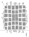
- Figure 5 shows a portion of a surface layer of a multilayer signal routing device having nine subarrays of electrically conductive contacts for mating with nine corresponding subarrays of electrically conductive contacts of a surface mount grid array package of an electronic component that is mounted on the surface of the multilayer signal routing device in accordance with an embodiment of the present invention.
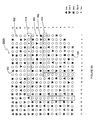
- Figure 6A shows a portion of a surface layer of a multilayer signal routing device having 330 electrically conductive contacts for mating with 330 corresponding electrically conductive contacts of a quadrant of a surface mount grid array package of an electronic component having a total of 1247 electrically conductive contacts that is mounted on the surface of the multilayer signal routing device in accordance with an embodiment of the present invention.
- Figure 6B shows a portion of a surface layer of a multilayer signal routing device having 330 electrically conductive contacts for mating with 330 corresponding electrically conductive contacts of a quadrant of a surface mount grid array package of an electronic component having a total of 1247 electrically conductive contacts that is mounted on the surface of the multilayer signal routing device in accordance with an embodiment of the present invention.
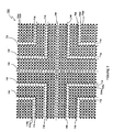
- Figure 7 shows a portion of a surface layer of a multilayer signal routing device having 952 electrically conductive contacts for mating with 952 corresponding electrically conductive contacts of a surface mount grid array package of an electronic component that is mounted on the surface of the multilayer signal routing device in accordance with an embodiment of the present invention.
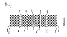
- Figure 8 shows a portion of a surface layer of a multilayer signal routing device having 196 electrically conductive contacts for mating with 196 corresponding electrically conductive contacts of a surface mount grid array package of an electronic connector component that is mounted on the surface of the multilayer signal routing device in accordance with an embodiment of the present invention.
- FIG. 1 there is shown a portion 100 of a surface layer of a multilayer signal routing device having 952 (i.e., a 28 x 34 array) electrically conductive contacts 102 for mating with 952 (i.e. , also a 28 x 34 array) corresponding electrically conductive contacts of a surface mount grid array package of an electronic component that is mounted on the surface of the multilayer signal routing device.
- 952 i.e., a 28 x 34 array
- 952 i.e., a 28 x 34 array
- the 952 electrically conductive contacts 102 may mate with 952 corresponding electrically conductive contacts of multiple surface mount grid array packages of multiple electronic components (or multichip modules or hybrid modules having multiple electronic components of like or differing kind) that are mounted on the surface of the multilayer signal routing device.
- Figure 1 also shows an electrically conductive contact/via 104 that is electrically connected to each of the electrically conductive contacts 102 on the surface layer of the multilayer signal routing device via a dog-bone configuration.
- the electrical connections between each of the electrically conductive contacts 102 and each respective electrically conductive contact/via 104 are not shown in Figure 1 for purposes of figure clarity.
- the letter designations associated with each numerical reference designator indicate which electrically conductive contact 102 is electrically connected to which respective electrically conductive contact/via 104.
- the array of electrically conductive contacts 102 may be divided into four quadrants (e.g., the a, b, c, & d quadrants).
- the four quadrants are separated via the dog-bone configuration by center channels 106, which are formed in the array of electrically conductive contacts 102, or, more appropriately, the array of electrically conductive contacts/vias 104, so as to allow electrical signals to be routed within these center channels 106 in one or more electrically conductive signal path layers of the multilayer signal routing device beneath corresponding ones of the electrically conductive contacts 102.
- FIG. 2 there is shown a portion 200 of a surface layer of a multilayer signal routing device having 1080 (i.e., a 30 x 36 array) electrically conductive contacts 202 for mating with 1080 (i.e., also a 30 x 36 array) corresponding electrically conductive contacts of a surface mount grid array package of an electronic component that is mounted on the surface of the multilayer signal routing device.
- 1080 i.e., a 30 x 36 array
- 1080 i.e., also a 30 x 36 array
- the 1080 electrically conductive contacts 202 may mate with 1080 corresponding electrically conductive contacts of multiple surface mount grid array packages of multiple electronic components (or multichip modules or hybrid modules having multiple electronic components of like or differing kind) that are mounted on the surface of the multilayer signal routing device.
- Figure 2 also shows an electrically conductive contact/via 204 that is electrically connected to each of the electrically conductive contacts 202 on the surface layer of the multilayer signal routing device via a dog-bone configuration.
- the electrical connections between each of the electrically conductive contacts 202 and each respective electrically conductive contact/via 204 are not shown in Figure 2 for purposes of figure clarity.
- the letter designations associated with each numerical reference designator indicate which electrically conductive contact 202 is electrically connected to which respective electrically conductive contact/via 204.
- the array of electrically conductive contacts 202 may be divided into four main quadrants (e.g., the a, b, c, & d main quadrants).
- the four main quadrants are separated via the dog-bone configuration by center channels 206, which are formed in the array of electrically conductive contacts 202, or, more appropriately, the array of electrically conductive contacts/vias 204, so as to allow electrical signals to be routed within these center channels 206 in one or more electrically conductive signal path layers of the multilayer signal routing device beneath corresponding ones of the electrically conductive contacts 202.
- Additional channels 208 are formed in each of the four main quadrants by eliminating rows and columns of electrically conductive contacts 202 in the array of electrically conductive contacts 202, and hence in the array of electrically conductive contacts/vias 204, so as to allow electrical signals to be routed within these additional channels 208 in one or more electrically conductive signal path layers of the multilayer signal routing device beneath corresponding ones of the electrically conductive contacts 202.
- corresponding rows and columns of electrically conductive contacts must be removed from the surface mount grid array package of the electronic component that is mounted on the surface of the multilayer signal routing device.
- one aspect of the present invention is to remove rows and columns of electrically conductive contacts from the surface mount grid array package of the electronic component that is mounted on the surface of the multilayer signal routing device so as to allow corresponding rows and columns of electrically conductive contacts 202 to be removed from the array of electrically conductive contacts 202, and hence the array of electrically conductive contacts/vias 204, thereby allowing additional channels 208 to be formed in the array of electrically conductive contacts 202, or, more appropriately, the array of electrically conductive contacts/vias 204, so as to allow electrical signals to be routed within these additional channels 208 in one or more electrically conductive signal path layers of the multilayer signal routing device beneath corresponding ones of the electrically conductive contacts 202.
- Figure 3 shows a portion 300 of a surface layer of a multilayer signal routing device having 952 (i.e., a 28 x 34 array) electrically conductive contacts 302 for mating with 952 (i.e., also a 28 x 34 array) corresponding electrically conductive contacts of a surface mount grid array package of an electronic component that is mounted on the surface of the multilayer signal routing device.
- 952 i.e., a 28 x 34 array
- 952 i.e., a 28 x 34 array
- the 952 electrically conductive contacts 302 may mate with 952 corresponding electrically conductive contacts of multiple surface mount grid array packages of multiple electronic components (or multichip modules or hybrid modules having multiple electronic components of like or differing kind) that are mounted on the surface of the multilayer signal routing device.
- Figure 3 also shows an electrically conductive contact/via 304 that is electrically connected to each of the electrically conductive contacts 302 on the surface layer of the multilayer signal routing device via a dog-bone configuration.
- the electrical connections between each of the electrically conductive contacts 302 and each respective electrically conductive contact/via 304 are not shown in Figure 3 for purposes of figure clarity.
- the letter designations associated with each numerical reference designator indicate which electrically conductive contact 302 is electrically connected to which respective electrically conductive contact/via 304.
- the array of electrically conductive contacts 302, or, more appropriately, the array of electrically conductive contacts/vias 304 may be divided into four main quadrants (e.g., the a, b, c, & d main quadrants).
- the four main quadrants are separated via the dog-bone configuration by center channels 306, which are formed in the array of electrically conductive contacts 302, or, more appropriately, the array of electrically conductive contacts/vias 304, so as to allow electrical signals to be routed within these center channels 306 in one or more electrically conductive signal path layers of the multilayer signal routing device beneath corresponding ones of the electrically conductive contacts 302.
- the center channels 306 are expanded from the center of the array of electrically conductive contacts 302 to the outer edges of the array of electrically conductive contacts 302.
- Additional channels 308 are again formed in each of the four main quadrants by eliminating rows and columns of electrically conductive contacts 302 in the array of electrically conductive contacts 302, and hence in the array of electrically conductive contacts/vias 304, so as to allow electrical signals to be routed within these additional channels 308 in one or more electrically conductive signal path layers of the multilayer signal routing device beneath corresponding ones of the electrically conductive contacts 302.
- the additional channels 308 are expanded from the center of the array of electrically conductive contacts 302 to the outer edges of the array of electrically conductive contacts 302.
- the expansion of the center channels 306 and the additional channels 308 from the center of the array of electrically conductive contacts 302 to the outer edges of the array of electrically conductive contacts 302 reduces any blocking effects which may be inflicted upon signal paths that are routed on one or more electrically conductive signal path layers of the multilayer signal routing device from the center of the array of electrically conductive contacts 302 by signal paths that are routed on one or more electrically conductive signal path layers of the multilayer signal routing device from the outer edges of the array of electrically conductive contacts 302.
- one aspect of the present invention is to remove rows and columns of electrically conductive contacts from the surface mount grid array package of the electronic component that is mounted on the surface of the multilayer signal routing device so as to allow corresponding rows and columns of electrically conductive contacts 302 to be removed from the array of electrically conductive contacts 302, and hence the array of electrically conductive contacts/vias 304, thereby allowing additional channels 308 to be formed in the array of electrically conductive contacts 302, or, more appropriately, the array of electrically conductive contacts/vias 304, so as to allow electrical signals to be routed within these additional channels 308 in one or more electrically conductive signal path layers of the multilayer signal routing device beneath corresponding ones of the electrically conductive contacts 302.
- Figure 4 shows a portion 400 of a surface layer of a multilayer signal routing device having 420 (i.e., 20 x 21 contact cells) electrically conductive contacts 402 for mating with 420 (i.e., also 20 x 21 contact cells) corresponding electrically conductive contacts of a surface mount grid array package of an electronic component that is mounted on the surface of the multilayer signal routing device.
- 420 i.e., 20 x 21 contact cells
- 420 i.e., also 20 x 21 contact cells
- the 402 electrically conductive contacts 402 may mate with 402 corresponding electrically conductive contacts of multiple surface mount grid array packages of multiple electronic components (or multichip modules or hybrid modules having multiple electronic components of like or differing kind) that are mounted on the surface of the multilayer signal routing device.
- Figure 4 also shows an electrically conductive contact/via 404 that is electrically connected to each of the electrically conductive contacts 402 on the surface layer of the multilayer signal routing device via a dog-bone configuration.
- the electrical connections between each of the electrically conductive contacts 402 and each respective electrically conductive contact/via 404 are not shown in Figure 4 for purposes of figure clarity.
- the letter designations associated with each numerical reference designator indicate which electrically conductive contact 402 is electrically connected to which respective electrically conductive contact/via 404.
- Figure 4 shows the array of electrically conductive contacts 402, and hence the array of electrically conductive contacts/vias 404, as a group of twenty twenty-one contact cells with each cell having a somewhat circular shape, it is within the scope of the present invention to allow any number of cell shapes and sizes (e.g., a square shape). Also, while Figure 4 shows the contact pattern of the array of electrically conductive contacts 402, and hence the array of electrically conductive contacts/vias 404, as being substantially square, it is within the scope of the present invention to allow any number of contact patterns (e.g., a triangular pattern).
- Figure 5 shows a portion 500 of a surface layer of a multilayer signal routing device having nine subarrays 510 (e.g., each having 1247 contacts) of electrically conductive contacts 502 for mating with nine corresponding subarrays of electrically conductive contacts of a surface mount grid array package of an electronic component that is mounted on the surface of the multilayer signal routing device.
- the electrically conductive contacts 502 may mate with corresponding electrically conductive contacts of multiple surface mount grid array packages of multiple electronic components (or multichip modules or hybrid modules having multiple electronic components of like or differing kind) that are mounted on the surface of the multilayer signal routing device.
- the electrically conductive contacts 502 have different shapes corresponding to different electrical properties (e.g., Signal, Ground, Power, and Test electrical properties) associated with the electrically conductive contacts 502.
- each subarray 510 has center channels 506 (light shaded) and additional channels 508 (dark shaded) formed therein.
- the nine subarrays 510 are sized and spaced so as to allow each subarray 510 to route electrical signals therebetween and within the center channels 506 and additional channels 508 formed therein in one or more electrically conductive signal path layers of the multilayer signal routing device.
- both Figure 6A and Figure 6B show a portion (600A and 600B, respectively) of a surface layer of a multilayer signal routing device having 330 electrically conductive contacts for mating with 330 corresponding electrically conductive contacts of a quadrant of a surface mount grid array package of an electronic component having a total of 1247 electrically conductive contacts that is mounted on the surface of the multilayer signal routing device.
- each of the electrically conductive contacts 602 may have one of several different types of electrical properties (e.g., Signal, Ground (GND), Power (Vdd, Vdd2), or Test).
- channels in one or more electrically conductive signal path layers of the multilayer signal routing device beneath electrically conductive contacts 602 that do not have electrical properties associated with Ground (GND) or Power (Vdd, Vdd2), as electrically conductive contacts 602 having Ground (GND) and Power (Vdd, Vdd2) electrical properties typically result in channel blockages (e.g., through hole vias).
- GND Ground
- Vdd Power
- the channels 614 are only proposed to be formed beneath electrically conductive contacts 602 that have electrical properties associated with Signal or Test, as electrically conductive contacts 602 having Signal or Test electrical properties require only surface signal routing or allow microvias to be utilized as discussed in the above-referenced U.S. Patent Application No. 10/126,700, U.S. Patent Application No. 09/651,188 (now U.S. Patent No. 6,388,890), and U.S. Provisional Patent Application No. 60/212,387, all of which have been incorporated by reference herein in their entirety.
- the electronic component that is mounted on the surface of the multilayer signal routing device should be designed with electrically conductive contacts having electrical properties that coincide with that shown in Figures 6A and 6B since such a contact pattern allows the clear orthogonal channels 614 to be formed in electrically conductive signal path layers of the multilayer signal routing device beneath electrically conductive contacts 602 that have electrical properties associated with Signal or Test.
- the electrically conductive contacts 602 that do not have electrical properties associated with Ground (GND) or Power (Vdd, Vdd2) are only cleared away from locations where channels should be formed.
- the electrically conductive contacts 602 that do not have electrical properties associated with Ground (GND) or Power (Vdd, Vdd2) are cleared away from rows and columns in a reasonably regular pattern that also aligns with where channels need to be formed.
- Figure 7 shows a portion 700 of a surface layer of a multilayer signal routing device having 952 (i.e., a 28 x 34 array) electrically conductive contacts 702 and 716 for mating with 952 (i.e., also a 28 x 34 array) corresponding electrically conductive contacts of a surface mount grid array package of an electronic component that is mounted on the surface of the multilayer signal routing device.
- 952 i.e., a 28 x 34 array
- 952 i.e., a 28 x 34 array
- the 952 electrically conductive contacts 702 and 716 may mate with 952 corresponding electrically conductive contacts of multiple surface mount grid array packages of multiple electronic components (or multichip modules or hybrid modules having multiple electronic components of like or differing kind) that are mounted on the surface of the multilayer signal routing device.
- Figure 7 also shows an electrically conductive contact/via 704 that is electrically connected to some of the electrically conductive contacts 702 on the surface layer of the multilayer signal routing device via a dog-bone configuration.
- the electrical connections between each of the electrically conductive contacts 702 and each respective electrically conductive contact/via 704 are not shown in Figure 7 for purposes of figure clarity.
- the letter designations associated with each numerical reference designator indicate which electrically conductive contact 702 is electrically connected to which respective electrically conductive contact/via 704.
- the array of electrically conductive contacts 702 (and 716), or, more appropriately, the array of electrically conductive contacts/vias 704, may be divided into four main quadrants (e.g., the a, b, c, & d main quadrants).
- the four main quadrants are separated via the dog-bone configuration by center channels 706, which are formed in the array of electrically conductive contacts 702 (and 716), or, more appropriately, the array of electrically conductive contacts/vias 704, so as to allow electrical signals to be routed within these center channels 706 in one or more electrically conductive signal path layers of the multilayer signal routing device beneath corresponding ones of the electrically conductive contacts 702.
- the electrically conductive contacts 716 are not electrically connected to respective ones of the electrically conductive contacts/vias 704.
- the electrically conductive contacts 716 are not electrically connected to anything and are commonly referred to as "no-connect" contacts. That is, the electronic component that is mounted on the surface of the multilayer signal routing device is designed with electrically conductive contacts that are not electrically connected to anything and are commonly referred to as "no-connect” contacts.
- these electrically conductive contacts of the electronic component that coincide with the electrically conductive contacts 716 formed on the surface layer of the multilayer signal routing device may be used only for factory testing electronic component.
- these "no-connect" contacts of the electronic component coincide with the electrically conductive contacts 716 formed on the surface layer of the multilayer signal routing device that are not electrically connected to anything. Since these electrically conductive contacts 716 are not connected to anything, additional channels 708 may be formed in electrically conductive signal path layers of the multilayer signal routing device beneath these electrically conductive contacts 716.
- the electrically conductive contacts 716 may be removed entirely from the surface layer of the multilayer signal routing device since they are not electrically connected to anything and the additional channels 708 may still be formed in electrically conductive signal path layers of the multilayer signal routing device beneath where these electrically conductive contacts 716 could have been formed.
- Figure 8 shows a portion 800 of a surface layer of a multilayer signal routing device having 196 (i.e., a 7 x 28 array) electrically conductive contacts 802 and 816 for mating with 196 (i.e., also a 7 x 28 array) corresponding electrically conductive contacts of a surface mount grid array package of an electronic connector component that is mounted on the surface of the multilayer signal routing device.
- 196 i.e., a 7 x 28 array
- electrically conductive contacts 802 and 816 for mating with 196 (i.e., also a 7 x 28 array) corresponding electrically conductive contacts of a surface mount grid array package of an electronic connector component that is mounted on the surface of the multilayer signal routing device.
- the 196 electrically conductive contacts 802 and 816 may mate with 196 corresponding electrically conductive contacts of multiple surface mount grid array packages of multiple electronic components (or multichip modules or hybrid modules having multiple electronic components of like or differing kind) that are mounted on the surface of the multilayer signal routing device.
- Figure 8 also shows an electrically conductive contact/via 804 that is electrically connected to some of the electrically conductive contacts 802 on the surface layer of the multilayer signal routing device via a dog-bone configuration.
- the electrical connections between each of the electrically conductive contacts 802 and each respective electrically conductive contact/via 804 are not shown in Figure 8 for purposes of figure clarity.
- the letter designations associated with each numerical reference designator indicate which electrically conductive contact 802 is electrically connected to which respective electrically conductive contact/via 804.
- the array of electrically conductive contacts 802 (and 816), or, more appropriately, the array of electrically conductive contacts/vias 804, may be divided into two main halves (e.g., the a and b halves). The two main halves are separated via the dog-bone configuration by a center channel 806, which is formed in the array of electrically conductive contacts 802 (and 816), or, more appropriately, the array of electrically conductive contacts/vias 804, so as to allow electrical signals to be routed within this center channel 806 in one or more electrically conductive signal path layers of the multilayer signal routing device beneath corresponding ones of the electrically conductive contacts 802.
- the electrically conductive contacts 816 are not electrically connected to respective ones of the electrically conductive contacts/vias 804.
- the electrically conductive contacts 816 are not electrically connected to anything and are commonly referred to as "no-connect” contacts. That is, the electronic connector component that is mounted on the surface of the multilayer signal routing device is provided with electrically conductive contacts that are not electrically connected to anything and are commonly referred to as “no-connect” contacts. These "no-connect" contacts of the electronic connector component coincide with the electrically conductive contacts 816 formed on the surface layer of the multilayer signal routing device that are not electrically connected to anything. Since these electrically conductive contacts 816 are not connected to anything, additional channels 808 may be formed in electrically conductive signal path layers of the multilayer signal routing device beneath these electrically conductive contacts 816.
- the electrically conductive contacts 816 may be removed entirely from the surface layer of the multilayer signal routing device since they are not electrically connected to anything and the additional channels 808 may still be formed in electrically conductive signal path layers of the multilayer signal routing device beneath where these electrically conductive contacts 816 could have been formed.
Landscapes
- Engineering & Computer Science (AREA)
- Microelectronics & Electronic Packaging (AREA)
- Production Of Multi-Layered Print Wiring Board (AREA)
- Connecting Device With Holders (AREA)
- Electric Connection Of Electric Components To Printed Circuits (AREA)
Applications Claiming Priority (2)
| Application Number | Priority Date | Filing Date | Title |
|---|---|---|---|
| US326079 | 1994-10-19 | ||
| US10/326,079 US20040003941A1 (en) | 2000-06-19 | 2002-12-23 | Technique for electrically interconnecting electrical signals between an electronic component and a multilayer signal routing device |
Publications (2)
| Publication Number | Publication Date |
|---|---|
| EP1434474A2 true EP1434474A2 (fr) | 2004-06-30 |
| EP1434474A3 EP1434474A3 (fr) | 2004-08-04 |
Family
ID=32468980
Family Applications (1)
| Application Number | Title | Priority Date | Filing Date |
|---|---|---|---|
| EP03394086A Withdrawn EP1434474A3 (fr) | 2002-12-23 | 2003-09-12 | Technique pour interconnecter électriquement des signaux électriques entre un composant électronique et un dispositif d'acheminement de signaux multicouche |
Country Status (6)
| Country | Link |
|---|---|
| US (1) | US20040003941A1 (fr) |
| EP (1) | EP1434474A3 (fr) |
| JP (1) | JP2004207741A (fr) |
| KR (1) | KR20040057895A (fr) |
| CN (1) | CN1510982A (fr) |
| CA (1) | CA2438922A1 (fr) |
Families Citing this family (8)
| Publication number | Priority date | Publication date | Assignee | Title |
|---|---|---|---|---|
| US7738259B2 (en) * | 2004-01-22 | 2010-06-15 | Alcatel Lucent | Shared via decoupling for area arrays components |
| US7081672B1 (en) * | 2005-03-07 | 2006-07-25 | Lsi Logic Corporation | Substrate via layout to improve bias humidity testing reliability |
| US8350375B2 (en) * | 2008-05-15 | 2013-01-08 | Lsi Logic Corporation | Flipchip bump patterns for efficient I-mesh power distribution schemes |
| US8093708B2 (en) * | 2009-07-06 | 2012-01-10 | Sony Ericsson Mobile Communications Ab | Semiconductor package having non-uniform contact arrangement |
| KR20120140096A (ko) * | 2011-06-20 | 2012-12-28 | 삼성전자주식회사 | 어레이 보드 패턴을 포함하는 워킹 패널 및 워킹 패널 세트 |
| EP2808890A4 (fr) * | 2012-01-27 | 2015-08-19 | Panasonic Corp | Carte de circuit imprimé multicouches |
| WO2020142656A1 (fr) | 2019-01-04 | 2020-07-09 | Engent, Inc. | Systèmes et procédés de placement précis de composants |
| CN115767904A (zh) * | 2022-11-18 | 2023-03-07 | 环旭(深圳)电子科创有限公司 | 多层电路板的自动摆放导通孔的设计方法 |
Family Cites Families (14)
| Publication number | Priority date | Publication date | Assignee | Title |
|---|---|---|---|---|
| US5490042A (en) * | 1992-08-10 | 1996-02-06 | Environmental Research Institute Of Michigan | Programmable silicon circuit board |
| US5784262A (en) * | 1995-11-06 | 1998-07-21 | Symbios, Inc. | Arrangement of pads and through-holes for semiconductor packages |
| US5650660A (en) * | 1995-12-20 | 1997-07-22 | Intel Corp | Circuit pattern for a ball grid array integrated circuit package |
| US6075711A (en) * | 1996-10-21 | 2000-06-13 | Alpine Microsystems, Inc. | System and method for routing connections of integrated circuits |
| US5847936A (en) * | 1997-06-20 | 1998-12-08 | Sun Microsystems, Inc. | Optimized routing scheme for an integrated circuit/printed circuit board |
| US6232564B1 (en) * | 1998-10-09 | 2001-05-15 | International Business Machines Corporation | Printed wiring board wireability enhancement |
| US6181004B1 (en) * | 1999-01-22 | 2001-01-30 | Jerry D. Koontz | Digital signal processing assembly and test method |
| US6407564B1 (en) * | 1999-08-04 | 2002-06-18 | Taiwan Semiconductor Manufacturing Co., Ltd. | Universal BGA board for failure analysis and method of using |
| US6256769B1 (en) * | 1999-09-30 | 2001-07-03 | Unisys Corporation | Printed circuit board routing techniques |
| JP3407025B2 (ja) * | 2000-06-08 | 2003-05-19 | Necエレクトロニクス株式会社 | 半導体装置及びその製造方法 |
| US6388890B1 (en) * | 2000-06-19 | 2002-05-14 | Nortel Networks Limited | Technique for reducing the number of layers in a multilayer circuit board |
| US6815621B2 (en) * | 2000-10-02 | 2004-11-09 | Samsung Electronics Co., Ltd. | Chip scale package, printed circuit board, and method of designing a printed circuit board |
| US20030043560A1 (en) * | 2001-06-15 | 2003-03-06 | Clarkson Robert Roy | Printed circuit board having a microelectronic semiconductor device mount area for trace routing therethrough |
| US6687133B1 (en) * | 2002-11-15 | 2004-02-03 | Lsi Logic Corporation | Ground plane on 2 layer PBGA |
-
2002
- 2002-12-23 US US10/326,079 patent/US20040003941A1/en not_active Abandoned
-
2003
- 2003-08-29 CA CA002438922A patent/CA2438922A1/fr not_active Abandoned
- 2003-08-29 KR KR1020030060094A patent/KR20040057895A/ko not_active Ceased
- 2003-09-12 EP EP03394086A patent/EP1434474A3/fr not_active Withdrawn
- 2003-09-25 CN CNA031594581A patent/CN1510982A/zh active Pending
- 2003-12-22 JP JP2003425376A patent/JP2004207741A/ja active Pending
Also Published As
| Publication number | Publication date |
|---|---|
| EP1434474A3 (fr) | 2004-08-04 |
| US20040003941A1 (en) | 2004-01-08 |
| CN1510982A (zh) | 2004-07-07 |
| JP2004207741A (ja) | 2004-07-22 |
| KR20040057895A (ko) | 2004-07-02 |
| CA2438922A1 (fr) | 2004-06-23 |
Similar Documents
| Publication | Publication Date | Title |
|---|---|---|
| US6388890B1 (en) | Technique for reducing the number of layers in a multilayer circuit board | |
| US7256354B2 (en) | Technique for reducing the number of layers in a multilayer circuit board | |
| EP2952074B1 (fr) | Carte de circuit imprimé comportant un routage décalé de signaux différentiels | |
| US7069650B2 (en) | Method for reducing the number of layers in a multilayer signal routing device | |
| US7630188B2 (en) | Conditioner with coplanar conductors | |
| US6011695A (en) | External bus interface printed circuit board routing for a ball grid array integrated circuit package | |
| US7095107B2 (en) | Ball assignment schemes for integrated circuit packages | |
| US7069646B2 (en) | Techniques for reducing the number of layers in a multilayer signal routing device | |
| MXPA01013012A (es) | Matriz y/o paquete de circuito integrado que tiene un arreglo de contacto de separacion variable para la maximizacion del numero de lineas de senal por capa de encaminamiento. | |
| EP1434474A2 (fr) | Technique pour interconnecter électriquement des signaux électriques entre un composant électronique et un dispositif d'acheminement de signaux multicouche | |
| US7683483B2 (en) | Electronic device with connection bumps | |
| KR20010021191A (ko) | 다층 회로 기판 | |
| US7107673B2 (en) | Technique for accommodating electronic components on a multiplayer signal routing device | |
| US5691569A (en) | Integrated circuit package that has a plurality of staggered pins | |
| EP1714530B1 (fr) | Procede pouvant augmenter une densite d'acheminement d'une carte de circuit imprime, et carte de circuit imprime de ce type | |
| US20090174072A1 (en) | Semiconductor system having bga package with radially ball-depopulated substrate zones and board with radial via zones | |
| EP1461985B1 (fr) | Technique pour loger des composants electroniques sur un dispositif de routage de signal multicouche | |
| US8013253B2 (en) | Electrical connection board and assembly of such a board and a semiconductor component comprising an integrated circuit chip | |
| HK1065437A (en) | Technique for electrically interconnecting electrical signals between an electronic component and a multilayer signal routing devices | |
| TW202612170A (zh) | 陣列天線裝置 | |
| JPH05315759A (ja) | 多層印刷配線基板の配線構造 | |
| HK1147641B (zh) | 减少信号布线设备中的层数的方法 | |
| HK1064253B (en) | Technique for reducing the number of layers in a multilayer circuit board | |
| HK1143271B (en) | Technique for accommodating electronic components on a multilayer signal routing device | |
| WO2009094024A1 (fr) | Dispositif électronique doté de bosses de connexion |
Legal Events
| Date | Code | Title | Description |
|---|---|---|---|
| PUAI | Public reference made under article 153(3) epc to a published international application that has entered the european phase |
Free format text: ORIGINAL CODE: 0009012 |
|
| PUAL | Search report despatched |
Free format text: ORIGINAL CODE: 0009013 |
|
| AK | Designated contracting states |
Kind code of ref document: A2 Designated state(s): AT BE BG CH CY CZ DE DK EE ES FI FR GB GR HU IE IT LI LU MC NL PT RO SE SI SK TR |
|
| AX | Request for extension of the european patent |
Extension state: AL LT LV MK |
|
| AK | Designated contracting states |
Kind code of ref document: A3 Designated state(s): AT BE BG CH CY CZ DE DK EE ES FI FR GB GR HU IE IT LI LU MC NL PT RO SE SI SK TR |
|
| AX | Request for extension of the european patent |
Extension state: AL LT LV MK |
|
| 17P | Request for examination filed |
Effective date: 20050204 |
|
| AKX | Designation fees paid |
Designated state(s): DE FR GB |
|
| RBV | Designated contracting states (corrected) |
Designated state(s): DE FR GB |
|
| STAA | Information on the status of an ep patent application or granted ep patent |
Free format text: STATUS: THE APPLICATION HAS BEEN WITHDRAWN |
|
| 18W | Application withdrawn |
Effective date: 20060810 |