EP1435535A2 - Faseroptisches Kopplungssystem und sein Herstellungsverfahren - Google Patents
Faseroptisches Kopplungssystem und sein Herstellungsverfahren Download PDFInfo
- Publication number
- EP1435535A2 EP1435535A2 EP03029662A EP03029662A EP1435535A2 EP 1435535 A2 EP1435535 A2 EP 1435535A2 EP 03029662 A EP03029662 A EP 03029662A EP 03029662 A EP03029662 A EP 03029662A EP 1435535 A2 EP1435535 A2 EP 1435535A2
- Authority
- EP
- European Patent Office
- Prior art keywords
- substrate
- fine
- optical fiber
- lenses
- lens
- Prior art date
- Legal status (The legal status is an assumption and is not a legal conclusion. Google has not performed a legal analysis and makes no representation as to the accuracy of the status listed.)
- Withdrawn
Links
Images


Classifications
-
- G—PHYSICS
- G02—OPTICS
- G02B—OPTICAL ELEMENTS, SYSTEMS OR APPARATUS
- G02B6/00—Light guides; Structural details of arrangements comprising light guides and other optical elements, e.g. couplings
- G02B6/24—Coupling light guides
- G02B6/42—Coupling light guides with opto-electronic elements
- G02B6/4201—Packages, e.g. shape, construction, internal or external details
- G02B6/4204—Packages, e.g. shape, construction, internal or external details the coupling comprising intermediate optical elements, e.g. lenses, holograms
- G02B6/4206—Optical features
Definitions
- the present invention relates to an optical fiber coupling system and, more particularly, to an optical fiber coupling system with a compact size capable of minimizing a beam loss and suitable for a mass production, and its manufacturing method.
- the application field is extended to a display using laser such as a CD-RW or a DVD-RAM, optical recording medium, or a large-screen projector, a laser wireless communication, a material processing using laser (welding, cutting and fine processing related to a semiconductor, or the like), an optical amplifier and a pumping light source used for a medical use or a military use.
- laser such as a CD-RW or a DVD-RAM, optical recording medium, or a large-screen projector
- a laser wireless communication a material processing using laser (welding, cutting and fine processing related to a semiconductor, or the like)
- an optical amplifier and a pumping light source used for a medical use or a military use.
- the pumping light source of a solid state laser the material processing and the medical laser, a high laser output more than a few Watt level is required.
- the pumping of the solid state laser is a critical and big application field for a high output diode laser.
- One method for obtaining such a high laser output is that a high output laser diode is formed in an array type for use.
- a high output laser diode is formed in an array type for use.
- several laser beams radiated from the laser diode array are coupled to each optical fiber corresponding to each laser diode, and the optical fiber array is bundled to be used as a light source for pumping, whereby a high laser output can be obtained with the beam emitted from the laser diode array.
- the optical fiber coupling system includes an optical fiber array having a suitable numerical aperture (NA) and a core diameter, and a refractive optical lens serving to collimate the diode array beam.
- NA numerical aperture
- refractive optical lens serving to collimate the diode array beam.
- the existing optical fiber coupling system including the refractive optical lens is a device designed for a beam form of a multi-mode high output diode laser.
- the existing optical fiber coupling system requires a complicate three-dimensional shaped lens structure and an optical system with a high performance.
- a spread angle of light radiated from the laser diode is determined depending on a structure of the laser diode.
- an light-spread angle is in the range of about 32 ⁇ 44 in a vertical direction, and about 8 ⁇ 12 in the horizontal direction. This is because the size of a transversal section of a semiconductor laser oscillation region is a few micrometer ( ⁇ m), that is, so small that the output light is radiated at a wide angle owing to a diffraction effect.
- an overall distribution of the horizontal mode of the output light is oval.
- a laser beam spread angle is to be reduced.
- the light spread angle can be reduced to obtain a high efficiency for the output terminal optical fiber.
- the light spread angles are different at the horizontal and vertical directions, so two lens surfaces are required.
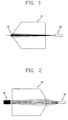
- Figures 1 and 2 show beam paths from a lens to an optical fiber of the output terminal according to a difference in the light spread angle in the horizontal and vertical directions of the general laser diode in a coupling optical system using a three-dimensional shaped lens in accordance with a conventional art.
- a lens R1 serves to collimate the laser beam with a wide light-spread angle radiated from the laser diode in a horizontal direction
- a lens R2 focuses laser beam radiated from the laser diode 10 in a side direction and makes it incident on a core, or a waveguide, of the optical fiber 20 of the output terminal.
- the optical fiber coupling system converts the form of beam radiated from the laser diode. Consequently, the lens R1 having a high numerical aperture collimates from an axis with a wide light-spread angle while the second-dimensional lens R2 projects an expanded light source to an axis with a smaller light-spread angle of the laser diode.
- a beam forming function of the optical fiber forms an almost circular spot at an inlet part of the optical fiber of the output terminal and can be used to pump laser mode.
- An efficiency of the structure is dependent upon the diode laser and the optical fiber as well as the optical system.
- the laser spread angle needs to be small as possible while the aperture of the optical fiber needs to be large, and the lenses of the optical system should be accurately aligned according to size.
- Light coming into the optical fiber with a small angle is totally, internally reflected from a core-cladding interface, and at this time, a portion of the totally-reflected light is absorbed, causing an output reduction.
- the optical fiber coupling optical system needs to be designed to accomplish a maximum coupling efficiency, and a light source including the optical fiber needs to be optimized.
- Lenses serving for collimation reduce a spread angle of laser beam radiated from the laser diode, and the smaller the diameter of the collimated beam is, the easier a laser pumping is at a solid state laser medium, which makes the number of the optical devices reduce and the energy density for pumping increase.
- the optical fiber used by being optically connected to the high output laser diode array, its numerical aperture is 0.16 ⁇ 0.39, and its core size is 100 ⁇ 600 um.
- the laser diode emitting light with the optical fiber having a small numerical aperture is significantly used for a medical, solid state laser pumping.
- a coupling optics used for such usage is fabricated as a product by molding a lens made of glass and replicating it.
- a high-priced lens is aligned with and attached to the laser diode, the collimated beam coming out through the lens is focused to the optical fiber after passing through several lenses or respectively focused to the optical fiber array positioned at regular intervals, to obtain a high output beam.
- the two methods are to use a high-priced lens having a complicate three-dimensional shape or a series of lens array, and in this respect, the three-dimensional lens are can be favored for a mass-production because it is fabricated in an injection form using a precisely-processed high-priced metal mold.
- fabrication of the metal mold is difficult and costly, and in addition, since the minimum size of the lens is limited to the minimum size of a tool for processing a curved surface of the lens of the metal mold, it is very difficult to make the coupling optical system very small (slim).
- an object of the present invention is to provide an optical fiber coupling system which is able to minimize beam loss, compact and suitable for a mass-production, and its manufacturing method.
- an optical fiber coupling system including: a substrate 110 having a predetermined area; a laser beam emitting unit 120 attached at one side of the substrate 110 and emitting beam; a first fine lens 130 insertedly fixed at a first mounting groove 111 formed on the substrate 110 and focusing or collimating vertical beam emitted from the light radiating unit 120; second fine lenses 140 protrusively formed on the substrate 110 and focusing or collimating horizontal beam emitted from the light radiating unit 120; and a beam output unit 150 insertedly fixed to a second mounting groove 112 formed on the substrate 110 and outputting beam focused or collimated by the first and second fine lenses.
- an optical fiber coupling system including: forming mounting grooves with a predetermined shape on a substrate 110 having a predetermined area; coating a thick film photosensitizer with a predetermined thickness on the substrate 110 and forming second fine lenses for focusing or collimating horizontal beam by photolithography; bonding a first fine lens for focusing or collimating vertical beam and an output terminal optical fiber for pumping beam into the mounting grooves of the substrate 110; and aligning and bonding laser diodes on the substrate 110.
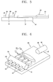
- Figure 3 is a perspective view showing an optical fiber coupling system in accordance with one embodiment of the present invention the present invention, and Figures 4 and 5 are plane view and front view showing the optical fiber coupling system.
- the optical fiber coupling system in accordance with one embodiment of the present invention includes: a substrate 110 having a predetermined area; a laser beam emitting unit 120 attached at one side of the substrate 110 and emitting beam; a first fine lens 130 insertedly fixed at a first mounting groove 111 formed on the substrate 110 and focusing or collimating vertical beam emitted from the light radiating unit 120; second fine lenses 140 protrusively formed on the substrate 110 and focusing or collimating horizontal beam emitted from the light radiating unit 120; and a beam output unit 150 insertedly fixed to a second mounting groove 112 formed on the substrate 110 and outputting beam focused or collimated by the first and second fine lenses.
- the first fine lens 130 and the second fine lenses 40 are positioned between the light radiation unit 120 and the beam output unit 150, and the first fine lens 130 is positioned at the side of the light radiating unit 120 while the second fine lenses 140 are positioned at the side of the beam output unit 150.
- the substrate 110 is formed with a predetermined thickness and an area with a square form.
- the substrate 110 is a silicon substrate 110.
- a first mounting groove 111 is formed at one side of the substrate 110, and a second mounting groove 112 is formed at the other side of the substrate 110.
- the first and second mounting grooves 111 and 112 have a predetermined length and an inverse triangular form in its section.
- the first mounting groove 111 is formed vertical to a longitudinal direction of the substrate 110 and the second mounting groove 112 is formed in a vertical direction of the first mounting groove 111, that is, in a longitudinal direction of the substrate 110.
- a plurality of second mounting grooves 112 are formed at regular intervals.
- the second fine lenses 140 are second-dimensional disk-type lenses 141 with predetermined thickness and shape. That is, the disk-type lens 141 has a rectangular shape with a predetermined thickness and one side there is formed in a semicircular shape. The semicircular side is positioned in a longitudinal direction of the substrate 110.
- the second fine lenses 140 are arranged at predetermined intervals at an upper surface of the substrate 110, protrusively formed at the upper surface of the substrate 110, and positioned in parallel next to the first mounting groove 111.
- the beam output unit 150 includes a plurality of output terminal optical fibers 151 positioned at the same line as the disk-type lenses 141.
- the second mounting grooves 112 are formed as many as the number of output terminal optical fibers 151 which are as many as the number of the second fine lenses 140.
- the plurality of output terminal optical fibers 151 are can be aligned to be bound to two or more-fold.
- the first fine lens 130 has a cylindrical form with a predetermined length and diameter, and is inserted into the first mounting groove 111 of the substrate 110 and fixed by an adhesive.
- the laser beam emitting unit 120 includes a plurality of laser diodes 121.
- the laser diodes 121 are arranged in a row parallel to the first fine lens 130, and attached to be fixed by an adhesive.
- the laser diode array 121 laser beam emitting unit, emits laser beam.
- the beam is an ovally emitted beam with different horizontal and vertical spread angles, which passes through the cylindrical lens, the first fine lens 130.
- the first fine lens 130 focuses the vertical beam with a wide spread angle in a spot form.
- the focused beam passes through the second fine lenses 140, that is, the second-dimensional lenses, and is respectively focused to the output terminal optical fibers 151.
- the second fine lenses 140 serve to collimate the horizontal beam and the collimated beam is focused to the output terminal optical fiber 151.
- the angle of the laser beam focused to the output terminal optical fiber 151 is controlled by adjusting a lens curvature of the second fine lens 140.
- the laser beam Passing through the output terminal optical fibers 151, the laser beam is collected to be used as a high output pumping source of solid state laser.
- the optical fiber coupling system as described above has such a structure that is able to heighten a focusing degree of laser beam as well as minimize an alignment error of an overall optical system.
- the substrate 110 and the second fine lenses 140 of the optical fiber coupling system can be manufactured by a MEMS (Micro Electro Mechanical System) technology which applies a lithographic technology and a micromachining technology. Accordingly, the optical fiber coupling system can be compact and can be fabricated by a mass-production structurally.
- MEMS Micro Electro Mechanical System
- Figure 6 is a perspective view showing an optical fiber coupling system in accordance with another embodiment of the present invention
- Figures 7 and 8 are plane view and front view showing the optical fiber coupling system.
- the optical fiber coupling system in accordance with another embodiment of the present invention includes: a substrate 110 having a predetermined area; a laser beam emitting unit 120 attached at one side of the substrate 110 and emitting beam; a first fine lens 130 insertedly fixed at a first mounting groove 111 formed on the substrate 110 and focusing or collimating vertical beam oscillated from the light radiating unit 120; second fine lenses 140 protrusively formed on the substrate 110 and focusing or collimating horizontal beam oscillated from the light radiating unit 120; and a beam output unit 150 insertedly fixed to a second mounting groove 112 formed on the substrate 110 and outputting beam focused or collimated by the first and second fine lenses.
- the laser beam emitting unit 120 and the first fine lens 130 fixed to the first mounting groove 111 of the substrate 110 have the same construction as those of the optical fiber coupling system of the former embodiment of the present invention.
- the second fine lenses 140 includes a second-dimensional disk-type lenses 141 having predetermined thickness and shape and a focusing lens 142 having predetermined thickness and oval shape.
- the second-dimensional disk-type lens 141 has a rectangular shape with a predetermined thickness and a semicircular shape in its side, and the semicircular side is positioned in a longitudinal direction of the substrate 110.
- the disk-type lenses 141 are arranged at predetermined intervals at an upper surface of the substrate 110, protrusively formed at the upper surface of the substrate 110, and positioned in parallel next to the first mounting groove 111.
- the focusing lens 142 is formed with two circular curved faces with a predetermined curvature, and the length of the circular curved face corresponds to the overall length of the disk-type lenses 141.
- the focusing lens 142 is positioned adjacent in parallel to the arrangement of the disk-type lenses 141, and extendedly protruded on the substrate 110.
- the beam output unit 150 is one output terminal optical fiber 151 positioned at a predetermined distance from the focusing lens 142.
- the output terminal optical fiber 151 is fixedly coupled to the second mounting groove 112 by an adhesive.
- the second mounting groove 112 in which the output terminal optical fiber 151 is mounted has a predetermined length and an inverse-triangular form in its section.
- the second mounting groove 112 is formed in a longitudinal direction of the substrate 110 and positioned at a central line of the focusing lens 142.
- the laser diode array 121 that is, the laser diode emitting unit 120, emits laser beam.
- the beam is an ovally emitted beam with different horizontal and vertical spread angles, which passes through the cylindrical lens, the first fine lens 130.
- the first fine lens 130 focuses the vertical beam with a wide spread angle in a spot form.
- the focused beam passes through the second fine lenses 140, that is, the disk-type lenses 141, and the focusing lens 142, and is respectively focused to the output terminal optical fibers 151.
- the disk-type lenses 141 serve to collimate the horizontal beam and the beams collimated respectively from the disk-type lenses 141 is focused as one beam to the output terminal optical fiber 151.
- the angle of the laser beam focused to the output terminal optical fiber 151 is controlled by adjusting a lens curvature of the second fine lens 140.
- the optical fiber coupling system as described above has such a structure that is able to heighten a focusing degree of laser beam as well as minimize an alignment error of an overall optical system.
- the substrate 110, the disk-type lenses 141, that is, the second fine lenses 140, and the focusing lens 142 constituting the optical fiber coupling system can be manufactured by a MEMS technology which applies a lithographic technology and a micromachining technology. Accordingly, the optical fiber coupling system can be compact and can be fabricated by a mass-production structurally.
- Figures 9A to 9D are front views sequentially showing a method for manufacturing the optical fiber coupling system.
- a method for manufacturing an optical fiber coupling system includes: forming mounting grooves 111 and 112 with a predetermined shape on a substrate 110 having a predetermined thickness and area; coating a thick film photosensitizer with a predetermined thickness on the substrate 110 and forming second fine lenses 140 for focusing or collimating horizontal beam by photolithography; bonding a first fine lens for focusing or collimating vertical beam and an output terminal optical fiber 151 for pumping beam into the mounting grooves 111 and 112 of the substrate 110; and aligning and bonding laser diodes 121 on the substrate 110.
- the substrate 110 is formed such that a silicon wafer having a crystal orientation is subjected to a cleaning process and then an etch mask for the mounting grooves is patterned through photolithography.
- the mounting grooves are respectively formed in a trench form.
- the mounting groove is formed in a trench by anisotropic wet etching with a chemical etching solution such as KOH, and subsequently, fine-processed by using a dry etching method such as a silicon deep reactive ion etching (RIE).
- RIE silicon deep reactive ion etching
- the depth of the mounting grooves 111 and 112 is determined depending on an outer diameter and length of the lenses mounted therein and an outer diameter of the output terminal optical fiber 151.
- the second fine lenses 140 are fabricated such that a thick film photosensitizer such as SU-8 or the like is coated with a predetermined thickness on the silicon substrate 110 and a photolithography process is performed thereon.
- the second fine lenses 140 includes a disk-type lens 141 having a predetermined height and formed with three plane faces and one curved face at its sections, and one focusing lens 142 having a predetermined height and an oval form.
- the disk-type lenses 142 and the focusing lens 142 are second-dimensional lenses with the same height and are adjacently positioned.
- the disk-type lenses 141 are formed in a row.
- the second fine lenses 140 may consist of the disk-type lenses 141 having a predetermined height and formed with three plane faces and one curved face at its sections,
- the disk-type lenses 141 are two-dimensional lenses with the same height and are arranged in a row.
- the second fine lenses 140 can be constructed in various forms.
- the second fine lenses 140 are fabricated by one time photolithography, and alignment of lenses are automatically made by the photolithography process.
- an anti-reflection coating layer (L) is formed on the second fine lenses 140.
- the anti-reflection coating layer (L) is formed entirely by a thin film deposition method such as a sputtering process or an evaporation process.
- the first fine lens 130 and the optical fiber 151 are positioned in the mounting grooves 111 and 112, respectively, and aligned and bonded by using a ultraviolet hardening resin adhesive or a thermosetting adhesive.
- the first fine lens 130 is a cylindrical lens having a predetermined length and outer diameter.
- the first fine lenses 130 and the output terminal optical fibers 151 are respectively positioned in the mounting grooves by a pick-and-place method.
- the laser diodes 121 are aligned and bonded to the silicon substrate 110 by using a silicon bulk micromachining process and a solder bonding technique.
- an intermediate layer made of Cu or the like having a high thermal conductivity can be inserted to a portion of the substrate 110 where the laser diodes 121 are mounted, in order to quickly release heat generated from the laser diode 121 in operation.
- the coupling optics focusing beams coming out of the laser diode array to one output terminal optical fiber 151 is integrated by using the lithography technology and the micromachining technology, so that an alignment error of the optical system can be reduced and beam focusing degree can be heightened.
- the optical fiber coupling system can be made compact, the number of assembly processes can be reduced, and a mass-production can be made.
- optical fiber coupling system and its manufacturing method of the present invention have the following advantages.
- optical fiber coupling system is made slim, its application coverage can be extended.
Landscapes
- Physics & Mathematics (AREA)
- General Physics & Mathematics (AREA)
- Optics & Photonics (AREA)
- Optical Couplings Of Light Guides (AREA)
- Semiconductor Lasers (AREA)
Applications Claiming Priority (4)
| Application Number | Priority Date | Filing Date | Title |
|---|---|---|---|
| KR1020020088392A KR20040062073A (ko) | 2002-12-31 | 2002-12-31 | 미세 렌즈 배열을 이용한 광섬유-결합기 |
| KR2002088392 | 2002-12-31 | ||
| KR10-2003-0048329A KR100539545B1 (ko) | 2003-07-15 | 2003-07-15 | 미세 광학 결합기 및 그 제조방법 |
| KR2003048329 | 2003-07-15 |
Publications (2)
| Publication Number | Publication Date |
|---|---|
| EP1435535A2 true EP1435535A2 (de) | 2004-07-07 |
| EP1435535A3 EP1435535A3 (de) | 2005-02-02 |
Family
ID=32510722
Family Applications (1)
| Application Number | Title | Priority Date | Filing Date |
|---|---|---|---|
| EP03029662A Withdrawn EP1435535A3 (de) | 2002-12-31 | 2003-12-23 | Faseroptisches Kopplungssystem und sein Herstellungsverfahren |
Country Status (4)
| Country | Link |
|---|---|
| US (1) | US7123791B2 (de) |
| EP (1) | EP1435535A3 (de) |
| JP (1) | JP2004213003A (de) |
| CN (1) | CN1514264A (de) |
Cited By (1)
| Publication number | Priority date | Publication date | Assignee | Title |
|---|---|---|---|---|
| EP1542048A1 (de) * | 2003-12-12 | 2005-06-15 | Lg Electronics Inc. | Mikrokollimierendes Linsensystem für die optische Übertragung |
Families Citing this family (15)
| Publication number | Priority date | Publication date | Assignee | Title |
|---|---|---|---|---|
| US7387954B2 (en) * | 2004-10-04 | 2008-06-17 | Semiconductor Energy Laboratory Co., Ltd. | Beam homogenizer, laser irradiation apparatus, and method for manufacturing semiconductor device |
| TWI254131B (en) * | 2005-01-06 | 2006-05-01 | Univ Tsinghua | Real-time monitoring system for arrayed micro prints and method for using said system |
| US7338218B2 (en) * | 2005-02-01 | 2008-03-04 | Ibiden Co., Ltd. | Optical module, method of manufacturing the optical module, and data communication system including the optical module |
| US7881355B2 (en) * | 2005-12-15 | 2011-02-01 | Mind Melters, Inc. | System and method for generating intense laser light from laser diode arrays |
| JP5686015B2 (ja) * | 2011-03-26 | 2015-03-18 | 富士通株式会社 | 光コネクタ及び光コネクタの製造方法 |
| JP6318554B2 (ja) * | 2013-11-07 | 2018-05-09 | セイコーエプソン株式会社 | 光源装置及びプロジェクター |
| JP2015153889A (ja) * | 2014-02-14 | 2015-08-24 | 三菱電機株式会社 | レーザ合成光学装置 |
| TWI510832B (zh) * | 2014-09-12 | 2015-12-01 | Applied Optoelectronics Inc | 光傳輸次組件及其製造方法 |
| CN108020926A (zh) * | 2018-02-07 | 2018-05-11 | 北京镭创高科光电科技有限公司 | 一种激光显示系统及其匀光装置 |
| CN108761982B (zh) * | 2018-04-28 | 2021-01-12 | 毅丰显示科技(深圳)有限公司 | 投影集光系统 |
| CN108508431B (zh) * | 2018-06-08 | 2024-04-26 | 上海禾赛科技有限公司 | 一种激光发射系统 |
| WO2019237581A1 (en) | 2018-06-13 | 2019-12-19 | Hesai Photonics Technology Co., Ltd. | Lidar systems and methods |
| CN111239931A (zh) * | 2018-11-01 | 2020-06-05 | 青岛海信宽带多媒体技术有限公司 | 一种光发射器的耦合方法及光发射器 |
| CN119097413A (zh) * | 2019-01-15 | 2024-12-10 | 波士顿科学医学有限公司 | 对准方法和工具 |
| US20220019034A1 (en) * | 2020-07-14 | 2022-01-20 | Waymo Llc | Stabilizing Power Output |
Family Cites Families (8)
| Publication number | Priority date | Publication date | Assignee | Title |
|---|---|---|---|---|
| GB2220501A (en) * | 1988-07-06 | 1990-01-10 | Plessey Co Plc | Coupling waveguides using transverse cylindrical lenses |
| JPH05164947A (ja) * | 1991-12-13 | 1993-06-29 | Nippon Telegr & Teleph Corp <Ntt> | 光結合装置およびその製造方法 |
| US5745153A (en) * | 1992-12-07 | 1998-04-28 | Eastman Kodak Company | Optical means for using diode laser arrays in laser multibeam printers and recorders |
| US5580471A (en) * | 1994-03-30 | 1996-12-03 | Panasonic Technologies, Inc. | Apparatus and method for material treatment and inspection using fiber-coupled laser diode |
| DE19613755A1 (de) * | 1996-04-06 | 1997-10-09 | Sel Alcatel Ag | Optisches Koppelelement |
| US5761234A (en) * | 1996-07-09 | 1998-06-02 | Sdl, Inc. | High power, reliable optical fiber pumping system with high redundancy for use in lightwave communication systems |
| US6157502A (en) * | 1998-07-02 | 2000-12-05 | Digital Optics Corporation | Optical bench circularizer having alignment indentations and associated methods |
| JP3932982B2 (ja) * | 2002-05-29 | 2007-06-20 | 株式会社豊田中央研究所 | 集光用光回路及び光源装置 |
-
2003
- 2003-12-23 EP EP03029662A patent/EP1435535A3/de not_active Withdrawn
- 2003-12-26 JP JP2003433093A patent/JP2004213003A/ja not_active Withdrawn
- 2003-12-29 US US10/745,680 patent/US7123791B2/en not_active Expired - Fee Related
- 2003-12-31 CN CNA2003101103717A patent/CN1514264A/zh active Pending
Cited By (1)
| Publication number | Priority date | Publication date | Assignee | Title |
|---|---|---|---|---|
| EP1542048A1 (de) * | 2003-12-12 | 2005-06-15 | Lg Electronics Inc. | Mikrokollimierendes Linsensystem für die optische Übertragung |
Also Published As
| Publication number | Publication date |
|---|---|
| US20040136651A1 (en) | 2004-07-15 |
| EP1435535A3 (de) | 2005-02-02 |
| US7123791B2 (en) | 2006-10-17 |
| CN1514264A (zh) | 2004-07-21 |
| JP2004213003A (ja) | 2004-07-29 |
Similar Documents
| Publication | Publication Date | Title |
|---|---|---|
| US7123791B2 (en) | Optical fiber coupling system and manufacturing method thereof | |
| CA2995292C (en) | Photonic chip having a monolithically integrated reflector unit and method of manufacturing a reflector unit | |
| US6722792B2 (en) | Optical interconnect with integral reflective surface and lens, system including the interconnect and method of forming the same | |
| CN100451709C (zh) | 高耦合效率光电模块 | |
| KR20080005351A (ko) | 광섬유 콜리메이터계, 광섬유 콜리메이터 어레이, 광섬유콜리메이터계 및 광섬유 콜리메이터 어레이계의 제조 방법 | |
| JP2004085717A (ja) | レンズ付き光ファイバ | |
| WO2007108508A1 (ja) | 光モジュール | |
| JP2001305376A (ja) | コリメータアレイ装置の設計方法及びこの方法によって作製されたコリメータアレイ装置 | |
| JP2007505747A (ja) | マイクロ構造デバイス及びその製造方法 | |
| US7110630B2 (en) | Optical element assembly and method of making the same | |
| EP3995872B1 (de) | Zweistufige optische kopplung mit erweitertem strahl | |
| JP2001021771A (ja) | 半導体光伝送モジュール | |
| JP4697698B2 (ja) | 光デバイスおよびその製造方法 | |
| Nakagawa et al. | Lens-coupled laser diode module integrated on silicon platform | |
| KR100539545B1 (ko) | 미세 광학 결합기 및 그 제조방법 | |
| JP4537796B2 (ja) | ビーム整形用光学系及びレーザ光源及びビーム整形用光学系の作成方法 | |
| JP2004101962A (ja) | 光モジュール | |
| JP2005070507A (ja) | 光モジュール及び光結合調心方法 | |
| JPS6338909A (ja) | レンズ付光フアイバ | |
| KR20040062073A (ko) | 미세 렌즈 배열을 이용한 광섬유-결합기 | |
| JP2005250480A (ja) | 光結合システム | |
| CN1771446A (zh) | 光束整形及降低将外部光源和光学器件连接至薄硅波导引起的损耗的实用方法 | |
| JP5387930B1 (ja) | 発光素子・光ファイバ結合モジュール及びその部品 | |
| KR100643466B1 (ko) | 실리콘 광학 벤치 및 이를 포함한 레이저 디스플레이광원 | |
| CN121618313B (zh) | 一种侧面泵浦的泵浦装置及其制备方法、芯片 |
Legal Events
| Date | Code | Title | Description |
|---|---|---|---|
| PUAI | Public reference made under article 153(3) epc to a published international application that has entered the european phase |
Free format text: ORIGINAL CODE: 0009012 |
|
| AK | Designated contracting states |
Kind code of ref document: A2 Designated state(s): AT BE BG CH CY CZ DE DK EE ES FI FR GB GR HU IE IT LI LU MC NL PT RO SE SI SK TR |
|
| AX | Request for extension of the european patent |
Extension state: AL LT LV MK |
|
| PUAL | Search report despatched |
Free format text: ORIGINAL CODE: 0009013 |
|
| AK | Designated contracting states |
Kind code of ref document: A3 Designated state(s): AT BE BG CH CY CZ DE DK EE ES FI FR GB GR HU IE IT LI LU MC NL PT RO SE SI SK TR |
|
| AX | Request for extension of the european patent |
Extension state: AL LT LV MK |
|
| 17P | Request for examination filed |
Effective date: 20050402 |
|
| AKX | Designation fees paid |
Designated state(s): AT BE BG CH CY CZ DE DK EE ES FI FR GB GR HU IE IT LI LU MC NL PT RO SE SI SK TR |
|
| 17Q | First examination report despatched |
Effective date: 20050830 |
|
| STAA | Information on the status of an ep patent application or granted ep patent |
Free format text: STATUS: THE APPLICATION IS DEEMED TO BE WITHDRAWN |
|
| 18D | Application deemed to be withdrawn |
Effective date: 20070209 |