EP1435536A2 - Optische Kopplungsvorrichtung, ihr Herstellungsverfahren,optische Kopplungsvorrichtungsanordnung und mit einer Linse versehene Faser in der Kopplungsvorrichtung - Google Patents
Optische Kopplungsvorrichtung, ihr Herstellungsverfahren,optische Kopplungsvorrichtungsanordnung und mit einer Linse versehene Faser in der Kopplungsvorrichtung Download PDFInfo
- Publication number
- EP1435536A2 EP1435536A2 EP03030016A EP03030016A EP1435536A2 EP 1435536 A2 EP1435536 A2 EP 1435536A2 EP 03030016 A EP03030016 A EP 03030016A EP 03030016 A EP03030016 A EP 03030016A EP 1435536 A2 EP1435536 A2 EP 1435536A2
- Authority
- EP
- European Patent Office
- Prior art keywords
- optical
- core
- coupling device
- light
- optical coupling
- Prior art date
- Legal status (The legal status is an assumption and is not a legal conclusion. Google has not performed a legal analysis and makes no representation as to the accuracy of the status listed.)
- Granted
Links
Images


Classifications
-
- G—PHYSICS
- G02—OPTICS
- G02B—OPTICAL ELEMENTS, SYSTEMS OR APPARATUS
- G02B6/00—Light guides; Structural details of arrangements comprising light guides and other optical elements, e.g. couplings
- G02B6/24—Coupling light guides
- G02B6/42—Coupling light guides with opto-electronic elements
-
- G—PHYSICS
- G02—OPTICS
- G02B—OPTICAL ELEMENTS, SYSTEMS OR APPARATUS
- G02B6/00—Light guides; Structural details of arrangements comprising light guides and other optical elements, e.g. couplings
- G02B6/24—Coupling light guides
- G02B6/42—Coupling light guides with opto-electronic elements
- G02B6/4201—Packages, e.g. shape, construction, internal or external details
- G02B6/4204—Packages, e.g. shape, construction, internal or external details the coupling comprising intermediate optical elements, e.g. lenses, holograms
- G02B6/4206—Optical features
Definitions
- the present invention relates generally to an optical device, and in particular, to an optical coupling device for coupling light into an optical waveguide device.
- optical coupling is very important to system stability, mass production, and cost reduction.
- small, easily aligned optical devices must be developed.
- One of the current optical devices having the most effective optical coupling characteristics is a lensed fiber.
- An optical fiber having a micro-lens, a polished end, or a laser micro-machined end each exhibit a coupling efficiency nearing 100%.
- light emitted from an LD is coupled directly to a fiber core.
- a working distance is very small, merely the diameter of the core.
- the working distance can be increased to about 20 ⁇ m using a tapered hemispherical-end fiber.
- a graded index multimode fiber end can increase the working distance up to 45 ⁇ m, though having loss up to a 4dB.
- a silica fiber having an aspherical end face can increase the working distance remarkably, up to 153 ⁇ m.
- axial and lateral misalignment must be relatively small, and the possibility of misalignment has a great impact on mass production and reproducibility of optical modules.
- a lensed fiber using an expanded-core fiber and a hemispherically-ended coreless fiber has a long working distance, it suffers a low coupling efficiency of about 4dB and a small lateral misalignment tolerance of about 1.5 ⁇ m.
- Another coupling device using a pair of graded index-fibers having hemispherical ends has a relatively long working distance of about 50 ⁇ m and a great coupling efficiency of 1.5dB. Yet, its misalignment tolerance is far smaller than that of other lensed fibers and thus only active alignment is allowed. All the above lensed fibers are very complex to fabricate and have low reproducibility.
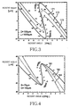
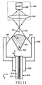
- FIG. 1 illustrates the structure of a conventional lensed fiber and FIGS. 2 to 5 depict the characteristics of the lensed fiber.
- an LD 140 is also illustrated.
- the LD is aligned with the lensed fiber 110 with respect to an optical axis 150.
- the lensed fiber 110 is divided into a single mode fiber 120 and a hemispherically ended coreless tip 130 connected to the single mode fiber 120.
- FIGs. 2, 3 and 4 it is impossible for the tip 130 to transfer all incident optical power to the single mode fiber 120 because of severe limitations on incident height h and incident angle ⁇ , each shown in Fig. 1.
- the more influential factor is incident height h.
- FIG. 2 illustrates incident angle-incident height curves 161, 162 and 163 when a working distance D is 130, 150 and 170 ⁇ m, respectively in the case where the end of the tip 130 has a curvature radius R of 75 ⁇ m and a length L of 1000 ⁇ m.
- the single mode fiber 120 has a thermally expanded core 125 at its end.
- This kind of single mode fiber 120 is characterized by its normalized frequency being maintained during fabrication. Therefore, the product of a maximum incident height and a maximum incident angle is kept as a constant during thermal expansion of the end of the core 125.
- Another parameter to consider in the single mode fiber 120, is that as a modal field diameter increases, the diameter of the end of the core 125 increases and a relative refraction index difference decreases.
- FIG. 5 illustrates an incident angle-incident height curve 191 of the thermally expanded core 125 and an incident angle-incident height curve 192 of a non-thermally expanded core (not shown).
- a larger amount of optical power can be coupled to the expanded core 125 under the above-described conditions.
- the end of the thermally expanded core 125 is similar to a tapered optical waveguide in many respects.
- the relative refractive index difference is drastically decreased during thermal expansion. For example, if the diameter of the section of the core end, as taken perpendicularly to a Z axis, increases from 4 to 16.8 ⁇ m, the relative refractive index difference falls from 0.356 to 0.02%.
- the conventional lensed fibers offer many benefits including high coupling efficiency, small size, and high stability. However, they have the shortcomings of complex fabrication and low reproducibility. Moreover, they have relatively short working distances and small lateral misalignment tolerances. What is worse, the conventional lensed fibers require precise, expensive tools such as V grooves to achieve high coupling efficiency.
- an object of the present invention to provide an optical coupling device, a fabricating method thereof, an optical coupling device assembly, and a lensed fiber using the optical coupling device, which are inexpensive and have a long working distance, a high coupling efficiency, and a large lateral misalignment tolerance.
- optical coupling device for coupling light to a core of an optical waveguide device, a fabrication method thereof, an optical coupling device assembly, and a lensed fiber using the optical coupling device.
- an opened housing has a hole in the bottom, and the optical waveguide device is inserted through the hole.
- An optical coupling device is fixed to the inner wall of the housing.
- a first end of the optical coupling device is connected to the core of the optical waveguide device, and a second end thereof is convex.
- the optical coupling device includes a conicle-shaped waveguide connecting both ends of the optical coupling device, for light transmission, and a cladding surrounding the waveguide.
- the lensed fiber has an optical fiber with a core and a cladding surrounding the core, and an optical coupling device.
- a first end of the optical coupling is connected to the core of the optical fiber and a second end is formed into a convex shape. It includes a conicle-shaped waveguide connecting the first and second ends of the optical coupling device, for light transmission, and a cladding surrounding the waveguide.
- the optical waveguide device is inserted into a hole formed in the bottom of a housing and a UV-cured mixture is filled in the housing.
- a conicle-shaped tapering part for converging UV light in the mixture is formed by irradiating UV light onto the surface of the mixture.
- a connecting part for connecting a narrow end of the tapering part to the core is grown by emitting the UV light through facing ends of the tapering part and the core.
- a cladding is formed by irradiating UV light onto the remaining non-cured mixture.
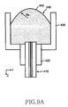
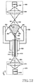
- FIG. 6 is a schematic view illustrating the configuration of an optical coupling device according to the present invention.
- an LD 250 and an optical waveguide device 240 are illustrated to describe the function of the optical coupling device 210.
- the LD 250 generates light 252 at a predetermined wavelength and emits the light 252 at a predetermined diffusion angle.
- the optical waveguide device 240 spaced from the LD 250 by a predetermined distance D+L, includes a core 242 being a light transmission path and a cladding 244 surrounding the core 242.
- the optical waveguide device 240 refers to an arbitrary device including a core as a light transmission path. Thus, it can be a single mode fiber drawn from an optical fiber preform, a planar lightwave circuit (PLC) formed by depositing a plurality of layers on a semiconductor substrate, an LD, or a photodiode.
- PLC planar lightwave circuit
- the optical coupling device 210 is spaced from the LD 250 by a predetermined distance D.
- the optical coupling device 210 has a first end 212 facing the LD 250, convex in a shape and having a predetermined curvature radius R from the center and a second end 214 opposite to the first end 212, the second end 214 being connected to the optical waveguide device 240.
- the optical coupling device 210 is comprised of a conicle or funnel-shaped waveguide 220 extending between the first and second ends 212 and 214, and a cladding 230 surrounding the waveguide 220.
- the waveguide 220 has a higher refractive index than the cladding 230.
- the waveguide 220 is divided into an conicle icicle-shaped tapering part 222 with a predetermined interior angle ⁇ and a connecting part 224 connecting the tapering part 222 to the core 242 of the optical waveguide device 240.
- the section of the tapering part 222 perpendicular to the Z axis becomes smaller from the first end 212 to the second end 214.
- the tapering part 222 serves to converge the light 252 to the convergence point 223 based on reflection of the light 252 at the boundary between the tapering part 222 and the cladding 230.
- the connecting part 224 couples the converged light 252 to the core 242 of the optical waveguide device 240.
- FIG. 7 is a flowchart illustrating a method of fabricating the optical coupling device according a preferred embodiment of the present invention
- FIGS. 8 to 14 are views sequentially illustrating the fabrication method of FIG. 7.
- the optical coupling device fabricating method includes preparation (step 310), alignment (step 350), and curing (step 360).
- step 310 an optical waveguide device is inserted through a hole formed in the bottom of a housing and a mixture is filled in the housing.
- the resultant is illustrated in FIG. 8.
- Step 310 is further branched into sub-steps 320, 330 and 340.
- an optical waveguide device 510 having a core 512 and a cladding 514 is fixedly inserted into a hole at the center of a holder 520.
- the optical waveguide device 510 protrudes at least 100 ⁇ m (shown as distance L 1 ) from the end of the holder 520.
- the optical waveguide device 510 can be an optical fiber or PLC, and a ferrule having a circular or square section perpendicular to the Z axis can be used as the holder 520.
- the holder 520 can be, for example, metal or plastic.
- the optical waveguide device 510 protrudes a predetermined length L 1 , preferably at least 100 ⁇ m from the end of the holder 520.
- the first optical system 550 is comprised of a first convex lens 554 and a first multi-wavelength light source (lamp 1) 552.
- the first multi-wavelength light source 552 is set to emit non-UV light 553 to prevent the mixture 540 from being cured. Preferably, it emits green light.
- a mercury lamp can be used as the first multi-wavelength light source 552 and a green filter can further be used to selectively emit green light from the mercury lamp.
- the light 553 emitted from the first multi-wavelength light source 552 is incident on the first convex lens 554, refracted therefrom, and then converged. The converged light is diffused and reaches the surface of the mixture 540.
- the optimal position tracing is done first to align the first optical system 550 with the housing 530 with respect to the optical axis 551 and then to decide a UV light focus for the curing step 360 using the first optical system 550.
- the first optical system 550 can be configured in various ways. It includes largely a lens system and the first multi-wavelength light source 552. As described before, the first multi-wavelength light source 552 can be a mercury lamp or a wavelength tunable laser that outputs visible rays and UV rays.
- the lens system determines the focus of the light 553 emitted from the first multi-wavelength light source 552 in conjunction with the surface 542 of the mixture 540. While the lens system is shown to have only the first convex lens 554 in FIG.
- a first convex lens collimates the light 553 emitted from the first multi-wavelength light source 552, and a second convex lens collects the collimated light.
- the light convergence position is altered by moving the second convex lens relative to the first convex lens and thus the focus of the light 553 is controlled by the surface 542 of the mixture 540.
- the lens system can also be configured using a holographic optical element (HOE) functioning as a lens. While the above alignment is implemented by moving the housing 530, the first optical system 550 can be moved wholly or partially, instead.
- HOE holographic optical element
- step 360 the mixture 540 is cured in step 360.
- This curing step 360 is further divided into first, second and third curing sub-steps 370, 380 and 390.
- the connecting part 564 is partially extended from the convergence point 563 of the tapering part 562 by means of the first optical system 550.
- the UV light 555 is irradiated onto the surface 542 of the mixture 540 by the first optical system, the UV light 555 is converged by the tapering part 562 and proceeds through the convergence point 563.
- the connecting part 564 is partially grown.
- the connecting part 564 is partially extended from the core 512 of the optical waveguide device 510 by the second optical system 570.
- the UV light 573 is coupled into the core 512 by the second optical system 570, the UV light 573 travels along the core 512 and then passes through the end of the core 512.
- the connecting part 564 is partially grown.
- FIG. 13 illustrates only a waveguide 560 produced in the second curing sub-step 380.
- the optical solder effect-based second curing sub-step 380 does not depend much on the alignment between the tapering part 562 and the optical waveguide device 510.
- the Z-axis length L 2 of the tapering part 562 is 1000 ⁇ m and an optical loss in the tapering part 562 is less than 1.5dB.
- the connecting part 564 undergoes an optical loss less than 0.5dB.
- the misalignment D 3 is dependent on the alignment state of the housing 530 and the growth state of the tapering part 562.
- a cladding is formed by curing the mixture 540 surrounding the waveguide 560 in the third curing sub-step 390. UV light can be irradiated to the mixture 540 in two ways.
- One way is to irradiate the UV light 555 onto the surface of the mixture 540.
- the first optical system 550 can be still used without much displacement. While the UV light is irradiated onto the center of the mixture surface 542 in the first or second curing sub-step 370 or 380, it must be irradiated onto the overall mixture surface 540. Therefore, a first optical system 550' free of the first convex lens is used.
- the other way is to irradiate the UV light 555 laterally onto the housing 530. It boasts of relatively uniform and rapid curing of the mixture 540.
- the housing 530 must be transparent to UV light, and it can be formed of a fused silica.
- UV light is irradiated with the first and second multi-wavelength light sources 552 and 572 or two light sources with different wavelengths positioned face to face at both sides of the housing 530.
- the UV light emitted from the first multi-wavelength light source 552 reaches all over the mixture surface 542.
- a cladding having a predetermined refractive index difference from the waveguide 560 is formed.
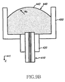
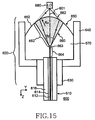
- FIG. 15 illustrates the configuration of a lensed fiber according to an embodiment of the present invention.
- an LD 680 is illustrated to describe the functionality of the lensed fiber 600.
- the LD 680 emits light 682 at a predetermined wavelength and the light 682 is diffused at a predetermined angle from the LD 680.
- the lensed fiber 600 includes a single mode fiber 610 and an optical coupling device assembly 620.
- the optical coupling device assembly 620 has a housing 640, a holder 630, and an optical coupling device 650.
- the single mode fiber 610 includes a core 612, a cladding 614 surrounding the core 612, and a coating 616 surrounding the cladding 614.
- the holder 630 is shaped into a hollow cylinder and the single mode fiber 610 is fixedly inserted into the holder 630, protruding from an end of the holder 630.
- the single mode fiber 610 can be fixed to the holder 630 in various ways. For example, an adhesive is filled in between the inner wall of the holder 630 and the single mode fiber 610.
- the optimal position of the LD 680 is on an optical axis 601 of the lensed fiber 600 and the focus of the light 682 emitted from the LD 680 coincides with a convergence point 663 of the tapering part 662. At this optimal position, the light 682 reaching the boundary of the tapering part 662 is totally reflected. Thus, reflection-incurred loss is minimized.
- the connecting part 664 couples the light 682 converged by the tapering part 662 into the core 612.
- FIG. 19 illustrates the configuration of a lensed fiber according to another embodiment of the present invention.
- a lensed fiber 700 is the same in configuration as that illustrated in FIG. 15 except for the material and fixing of a housing 740 and a holder 730. The following description is made mainly of this difference.
Landscapes
- Physics & Mathematics (AREA)
- General Physics & Mathematics (AREA)
- Optics & Photonics (AREA)
- Optical Couplings Of Light Guides (AREA)
Applications Claiming Priority (2)
| Application Number | Priority Date | Filing Date | Title |
|---|---|---|---|
| KR10-2002-0087991A KR100448968B1 (ko) | 2002-12-31 | 2002-12-31 | 광결합 소자의 제작 방법, 광결합 소자, 광결합 소자조립체 및 광결합 소자를 이용한 렌즈 결합형 광섬유 |
| KR2002087991 | 2002-12-31 |
Publications (3)
| Publication Number | Publication Date |
|---|---|
| EP1435536A2 true EP1435536A2 (de) | 2004-07-07 |
| EP1435536A3 EP1435536A3 (de) | 2004-12-22 |
| EP1435536B1 EP1435536B1 (de) | 2007-04-11 |
Family
ID=32501465
Family Applications (1)
| Application Number | Title | Priority Date | Filing Date |
|---|---|---|---|
| EP03030016A Expired - Lifetime EP1435536B1 (de) | 2002-12-31 | 2003-12-30 | Optische Kopplungsvorrichtung und ihr Herstellungsverfahren |
Country Status (6)
| Country | Link |
|---|---|
| US (1) | US7113671B2 (de) |
| EP (1) | EP1435536B1 (de) |
| JP (1) | JP3863144B2 (de) |
| KR (1) | KR100448968B1 (de) |
| CN (1) | CN1246717C (de) |
| DE (1) | DE60313113T2 (de) |
Cited By (3)
| Publication number | Priority date | Publication date | Assignee | Title |
|---|---|---|---|---|
| EP1703601A1 (de) * | 2005-03-15 | 2006-09-20 | Jtekt Corporation | Faserlaseroszillator |
| EP2056144A1 (de) * | 2007-10-31 | 2009-05-06 | Highyag Lasertechnologie GmbH | Endstück für Lichtleitfaser |
| GB2535803A (en) * | 2015-02-27 | 2016-08-31 | Gooch & Housego Plc | Fibre collimator |
Families Citing this family (19)
| Publication number | Priority date | Publication date | Assignee | Title |
|---|---|---|---|---|
| US7787106B2 (en) * | 2005-10-28 | 2010-08-31 | The United States Of America As Represented By The Department Of Health And Human Services | Particle image velocimetry system having an improved hollow-waveguide-based laser illumination system |
| US20090041412A1 (en) * | 2007-08-07 | 2009-02-12 | Jeffrey Dean Danley | Laser erosion processes for fiber optic ferrules |
| JP2009139895A (ja) * | 2007-12-11 | 2009-06-25 | Sumitomo Electric Ind Ltd | 光モジュールおよび光モジュールの製造方法 |
| WO2010138700A1 (en) * | 2009-05-29 | 2010-12-02 | Corning Cable Systems Llc | Dust cap assembly for sealing an optical fiber ferrule and methods thereof |
| US20110110627A1 (en) * | 2009-11-07 | 2011-05-12 | Dr. Chang Ching TSAI | Beam collimator |
| CN102162883A (zh) * | 2011-03-17 | 2011-08-24 | 武汉电信器件有限公司 | 光斑耦合转换装置 |
| CN103091790B (zh) * | 2011-10-28 | 2014-12-24 | 上海数字电视国家工程研究中心有限公司 | Led光源光纤连接器 |
| CN102681109B (zh) * | 2012-05-09 | 2014-07-09 | 天津大学 | 一种大口径光束耦合器 |
| US9383531B2 (en) * | 2013-04-23 | 2016-07-05 | Hon Hai Precision Industry Co., Ltd. | Light signal gathering device and optical module used thereof |
| JP2014222264A (ja) * | 2013-05-13 | 2014-11-27 | 株式会社オートネットワーク技術研究所 | 光コネクタ |
| JP2015102711A (ja) * | 2013-11-26 | 2015-06-04 | 矢崎総業株式会社 | 光ファイバの端部構造 |
| US9690055B2 (en) * | 2014-06-13 | 2017-06-27 | Corning Optical Communications LLC | Laser-based systems and methods for fiber-to-ferrule bonding for optical fiber connectors |
| CN104023100B (zh) * | 2014-06-26 | 2018-11-09 | 宇龙计算机通信科技(深圳)有限公司 | 一种移动设备及一种机身前壳 |
| CN104570237A (zh) * | 2014-12-19 | 2015-04-29 | 河北四方通信设备有限公司 | 光纤接口组件及其制作工艺 |
| US10439720B2 (en) * | 2017-05-19 | 2019-10-08 | Adolite Inc. | FPC-based optical interconnect module on glass interposer |
| CN110007400A (zh) * | 2018-01-04 | 2019-07-12 | 苏州旭创科技有限公司 | 光波导模式转换器、光学组件及其制造方法 |
| CN109765656A (zh) * | 2019-03-07 | 2019-05-17 | 深圳市艾孚光电科技有限公司 | 扩束多模光纤透镜及制作方法 |
| CN113467015B (zh) * | 2021-08-03 | 2023-03-21 | 新疆师范大学 | 一种激光器耦合台的中心校准装置 |
| CN114839721B (zh) * | 2022-04-15 | 2023-12-05 | 苏州苏驼通信科技股份有限公司 | 一种光线耦合适配器、方法、装置及电子设备 |
Family Cites Families (11)
| Publication number | Priority date | Publication date | Assignee | Title |
|---|---|---|---|---|
| DE3605659A1 (de) | 1986-02-21 | 1987-08-27 | Standard Elektrik Lorenz Ag | Ankoppeloptik fuer lichtwellenleiter |
| US4844580A (en) * | 1988-05-16 | 1989-07-04 | Gte Products Corporation | Fiber optic lens |
| JPH0777637A (ja) | 1993-09-08 | 1995-03-20 | Fujitsu Ltd | 光学素子結合方法及び屈折率像形成材料 |
| KR0126247B1 (en) | 1992-11-09 | 1997-12-26 | Fujitsu Ltd | Method of coupling optical parts and refractive index imaging material |
| JP3050271B2 (ja) * | 1994-06-03 | 2000-06-12 | 和雄 吉野 | 太陽光集光装置 |
| JPH0915448A (ja) | 1995-06-26 | 1997-01-17 | Takahisa Jitsuno | 光ファイバコネクタ及びその製造方法 |
| JP2002536683A (ja) | 1999-02-05 | 2002-10-29 | コーニング インコーポレイテッド | 造形された光学要素を有する光ファイバ部材およびその製造方法 |
| EP1228387A1 (de) | 1999-11-09 | 2002-08-07 | Corning Incorporated | Modenanpassung für mehrmoden-lichtleitfasersysteme |
| US6625351B2 (en) | 2000-02-17 | 2003-09-23 | Microfab Technologies, Inc. | Ink-jet printing of collimating microlenses onto optical fibers |
| JP3569493B2 (ja) | 2000-12-22 | 2004-09-22 | 日本非球面レンズ株式会社 | レンズ面の形成方法および形成装置 |
| US7218812B2 (en) * | 2003-10-27 | 2007-05-15 | Rpo Pty Limited | Planar waveguide with patterned cladding and method for producing the same |
-
2002
- 2002-12-31 KR KR10-2002-0087991A patent/KR100448968B1/ko not_active Expired - Fee Related
-
2003
- 2003-12-22 US US10/742,960 patent/US7113671B2/en not_active Expired - Lifetime
- 2003-12-26 JP JP2003435259A patent/JP3863144B2/ja not_active Expired - Fee Related
- 2003-12-30 CN CNB2003101243549A patent/CN1246717C/zh not_active Expired - Fee Related
- 2003-12-30 EP EP03030016A patent/EP1435536B1/de not_active Expired - Lifetime
- 2003-12-30 DE DE60313113T patent/DE60313113T2/de not_active Expired - Fee Related
Cited By (4)
| Publication number | Priority date | Publication date | Assignee | Title |
|---|---|---|---|---|
| EP1703601A1 (de) * | 2005-03-15 | 2006-09-20 | Jtekt Corporation | Faserlaseroszillator |
| EP2056144A1 (de) * | 2007-10-31 | 2009-05-06 | Highyag Lasertechnologie GmbH | Endstück für Lichtleitfaser |
| GB2535803A (en) * | 2015-02-27 | 2016-08-31 | Gooch & Housego Plc | Fibre collimator |
| GB2535803B (en) * | 2015-02-27 | 2019-01-23 | Gooch & Housego Torquay Ltd | Fibre collimator |
Also Published As
| Publication number | Publication date |
|---|---|
| US7113671B2 (en) | 2006-09-26 |
| JP3863144B2 (ja) | 2006-12-27 |
| EP1435536A3 (de) | 2004-12-22 |
| JP2004213008A (ja) | 2004-07-29 |
| KR20040061704A (ko) | 2004-07-07 |
| CN1514265A (zh) | 2004-07-21 |
| DE60313113D1 (de) | 2007-05-24 |
| DE60313113T2 (de) | 2007-08-09 |
| KR100448968B1 (ko) | 2004-09-18 |
| US20040131311A1 (en) | 2004-07-08 |
| EP1435536B1 (de) | 2007-04-11 |
| CN1246717C (zh) | 2006-03-22 |
Similar Documents
| Publication | Publication Date | Title |
|---|---|---|
| EP1435536B1 (de) | Optische Kopplungsvorrichtung und ihr Herstellungsverfahren | |
| KR100822953B1 (ko) | 광 도파관 렌즈 및 그 제조방법 | |
| US6847770B2 (en) | Lens function-including optical fiber and method of producing the same | |
| KR100276968B1 (ko) | 정렬 허용공차를 확대시킬 수 있는 광 연결구조 | |
| US6782162B2 (en) | Optical module and method for assembling the same | |
| US5278929A (en) | Optical module, method for fabricating the same and optical module unit with the same | |
| JP3726640B2 (ja) | 発光装置 | |
| EP0872747B1 (de) | Optisches Modul | |
| EP1298459A2 (de) | Asphärische Stablinse und zugehöriges Herstellungsverfahren | |
| JP2001350037A (ja) | レンズ部付プラスチック光ファイバ、光ファイバ結合器、その接続構造、及び接続方法 | |
| US7155096B2 (en) | Optical collimator for monomode fibers; monomode fiber with integrated collimator and method for making same | |
| US7874741B2 (en) | Optical module and process for manufacturing the same | |
| US20090016683A1 (en) | Angled fiber ferrule having off-axis fiber through-hole and method of coupling an optical fiber at an off-axis angle | |
| JP2008098316A (ja) | 半導体レーザモジュール | |
| JPH05281443A (ja) | 光結合方法 | |
| US11953737B2 (en) | Systems and methods for coupling light | |
| US6161965A (en) | Optical coupling circuit | |
| CN110646895B (zh) | 光插座及光收发器 | |
| US7653274B2 (en) | Optoelectric subassembly | |
| JP5387930B1 (ja) | 発光素子・光ファイバ結合モジュール及びその部品 | |
| JP2003066252A (ja) | コリメートレンズファイバー | |
| JPH02210406A (ja) | 光結合回路 | |
| JPH0515316B2 (de) | ||
| HK1116933A (en) | A laser module semiconductor | |
| Xuefeng et al. | Efficiency and optical feedback of traveling-wave semiconductor laser amplifier to single-mode fiber coupling: theory and experiment |
Legal Events
| Date | Code | Title | Description |
|---|---|---|---|
| PUAI | Public reference made under article 153(3) epc to a published international application that has entered the european phase |
Free format text: ORIGINAL CODE: 0009012 |
|
| 17P | Request for examination filed |
Effective date: 20031230 |
|
| AK | Designated contracting states |
Kind code of ref document: A2 Designated state(s): AT BE BG CH CY CZ DE DK EE ES FI FR GB GR HU IE IT LI LU MC NL PT RO SE SI SK TR |
|
| AX | Request for extension of the european patent |
Extension state: AL LT LV MK |
|
| PUAL | Search report despatched |
Free format text: ORIGINAL CODE: 0009013 |
|
| AK | Designated contracting states |
Kind code of ref document: A3 Designated state(s): AT BE BG CH CY CZ DE DK EE ES FI FR GB GR HU IE IT LI LU MC NL PT RO SE SI SK TR |
|
| AX | Request for extension of the european patent |
Extension state: AL LT LV MK |
|
| AKX | Designation fees paid |
Designated state(s): DE FI FR GB IT NL |
|
| GRAP | Despatch of communication of intention to grant a patent |
Free format text: ORIGINAL CODE: EPIDOSNIGR1 |
|
| RTI1 | Title (correction) |
Free format text: OPTICAL COUPLING DEVICE AND FABRICATING METHOD THEREOF |
|
| GRAS | Grant fee paid |
Free format text: ORIGINAL CODE: EPIDOSNIGR3 |
|
| GRAA | (expected) grant |
Free format text: ORIGINAL CODE: 0009210 |
|
| AK | Designated contracting states |
Kind code of ref document: B1 Designated state(s): DE FI FR GB IT NL |
|
| REG | Reference to a national code |
Ref country code: GB Ref legal event code: FG4D |
|
| REF | Corresponds to: |
Ref document number: 60313113 Country of ref document: DE Date of ref document: 20070524 Kind code of ref document: P |
|
| ET | Fr: translation filed | ||
| PLBE | No opposition filed within time limit |
Free format text: ORIGINAL CODE: 0009261 |
|
| STAA | Information on the status of an ep patent application or granted ep patent |
Free format text: STATUS: NO OPPOSITION FILED WITHIN TIME LIMIT |
|
| 26N | No opposition filed |
Effective date: 20080114 |
|
| PGFP | Annual fee paid to national office [announced via postgrant information from national office to epo] |
Ref country code: NL Payment date: 20081203 Year of fee payment: 6 |
|
| PGFP | Annual fee paid to national office [announced via postgrant information from national office to epo] |
Ref country code: FI Payment date: 20081212 Year of fee payment: 6 |
|
| PGFP | Annual fee paid to national office [announced via postgrant information from national office to epo] |
Ref country code: IT Payment date: 20081222 Year of fee payment: 6 |
|
| PGFP | Annual fee paid to national office [announced via postgrant information from national office to epo] |
Ref country code: FR Payment date: 20081212 Year of fee payment: 6 |
|
| PGFP | Annual fee paid to national office [announced via postgrant information from national office to epo] |
Ref country code: DE Payment date: 20090123 Year of fee payment: 6 |
|
| PGFP | Annual fee paid to national office [announced via postgrant information from national office to epo] |
Ref country code: GB Payment date: 20090122 Year of fee payment: 6 |
|
| REG | Reference to a national code |
Ref country code: NL Ref legal event code: V1 Effective date: 20100701 |
|
| GBPC | Gb: european patent ceased through non-payment of renewal fee |
Effective date: 20091230 |
|
| PG25 | Lapsed in a contracting state [announced via postgrant information from national office to epo] |
Ref country code: FI Free format text: LAPSE BECAUSE OF NON-PAYMENT OF DUE FEES Effective date: 20091230 |
|
| REG | Reference to a national code |
Ref country code: FR Ref legal event code: ST Effective date: 20100831 |
|
| PG25 | Lapsed in a contracting state [announced via postgrant information from national office to epo] |
Ref country code: NL Free format text: LAPSE BECAUSE OF NON-PAYMENT OF DUE FEES Effective date: 20100701 Ref country code: FR Free format text: LAPSE BECAUSE OF NON-PAYMENT OF DUE FEES Effective date: 20091231 |
|
| PG25 | Lapsed in a contracting state [announced via postgrant information from national office to epo] |
Ref country code: DE Free format text: LAPSE BECAUSE OF NON-PAYMENT OF DUE FEES Effective date: 20100701 |
|
| PG25 | Lapsed in a contracting state [announced via postgrant information from national office to epo] |
Ref country code: GB Free format text: LAPSE BECAUSE OF NON-PAYMENT OF DUE FEES Effective date: 20091230 |
|
| PG25 | Lapsed in a contracting state [announced via postgrant information from national office to epo] |
Ref country code: IT Free format text: LAPSE BECAUSE OF NON-PAYMENT OF DUE FEES Effective date: 20091230 |