EP1435687A1 - Recepteur à conversion directe - Google Patents
Recepteur à conversion directe Download PDFInfo
- Publication number
- EP1435687A1 EP1435687A1 EP02360380A EP02360380A EP1435687A1 EP 1435687 A1 EP1435687 A1 EP 1435687A1 EP 02360380 A EP02360380 A EP 02360380A EP 02360380 A EP02360380 A EP 02360380A EP 1435687 A1 EP1435687 A1 EP 1435687A1
- Authority
- EP
- European Patent Office
- Prior art keywords
- carrier signal
- signal
- image
- output
- compensator
- Prior art date
- Legal status (The legal status is an assumption and is not a legal conclusion. Google has not performed a legal analysis and makes no representation as to the accuracy of the status listed.)
- Granted
Links
- 238000006243 chemical reaction Methods 0.000 title claims abstract description 40
- 238000000034 method Methods 0.000 claims description 22
- 238000004590 computer program Methods 0.000 claims description 5
- 239000000969 carrier Substances 0.000 description 9
- 230000006978 adaptation Effects 0.000 description 4
- 230000000694 effects Effects 0.000 description 3
- 108010076504 Protein Sorting Signals Proteins 0.000 description 2
- 238000004422 calculation algorithm Methods 0.000 description 2
- 238000010276 construction Methods 0.000 description 2
- 244000187656 Eucalyptus cornuta Species 0.000 description 1
- 230000005540 biological transmission Effects 0.000 description 1
- 238000004364 calculation method Methods 0.000 description 1
- 238000004140 cleaning Methods 0.000 description 1
- 230000007547 defect Effects 0.000 description 1
- 230000006735 deficit Effects 0.000 description 1
- 230000001419 dependent effect Effects 0.000 description 1
- 238000012804 iterative process Methods 0.000 description 1
- 238000005070 sampling Methods 0.000 description 1
- 238000000926 separation method Methods 0.000 description 1
- 230000001629 suppression Effects 0.000 description 1
- 230000017105 transposition Effects 0.000 description 1
Images

Classifications
-
- H—ELECTRICITY
- H04—ELECTRIC COMMUNICATION TECHNIQUE
- H04L—TRANSMISSION OF DIGITAL INFORMATION, e.g. TELEGRAPHIC COMMUNICATION
- H04L27/00—Modulated-carrier systems
- H04L27/26—Systems using multi-frequency codes
- H04L27/2601—Multicarrier modulation systems
- H04L27/2647—Arrangements specific to the receiver only
-
- H—ELECTRICITY
- H03—ELECTRONIC CIRCUITRY
- H03D—DEMODULATION OR TRANSFERENCE OF MODULATION FROM ONE CARRIER TO ANOTHER
- H03D3/00—Demodulation of angle-, frequency- or phase- modulated oscillations
- H03D3/007—Demodulation of angle-, frequency- or phase- modulated oscillations by converting the oscillations into two quadrature related signals
-
- H—ELECTRICITY
- H04—ELECTRIC COMMUNICATION TECHNIQUE
- H04B—TRANSMISSION
- H04B1/00—Details of transmission systems, not covered by a single one of groups H04B3/00 - H04B13/00; Details of transmission systems not characterised by the medium used for transmission
- H04B1/06—Receivers
- H04B1/16—Circuits
- H04B1/30—Circuits for homodyne or synchrodyne receivers
-
- H—ELECTRICITY
- H04—ELECTRIC COMMUNICATION TECHNIQUE
- H04L—TRANSMISSION OF DIGITAL INFORMATION, e.g. TELEGRAPHIC COMMUNICATION
- H04L27/00—Modulated-carrier systems
- H04L27/32—Carrier systems characterised by combinations of two or more of the types covered by groups H04L27/02, H04L27/10, H04L27/18 or H04L27/26
- H04L27/34—Amplitude- and phase-modulated carrier systems, e.g. quadrature-amplitude modulated carrier systems
- H04L27/38—Demodulator circuits; Receiver circuits
- H04L27/3845—Demodulator circuits; Receiver circuits using non - coherent demodulation, i.e. not using a phase synchronous carrier
- H04L27/3854—Demodulator circuits; Receiver circuits using non - coherent demodulation, i.e. not using a phase synchronous carrier using a non - coherent carrier, including systems with baseband correction for phase or frequency offset
Definitions
- the invention relates to a direct conversion receiver DCR for receiving a multi-carrier signal including at least a first and a second carrier signal, being located at a first and second image carrier frequency, respectively, via an antenna.
- the invention further relates to a method for receiving such a multi-carrier signal, a computer program for carrying out such a method and an error estimating unit as well as to a compensator stage of such a direct conversion receiver.
- Direct conversion receivers DCR are substantially known in the art. They typically comprise a front end unit for receiving the multi-carrier signal from the antenna and a quadrature demodulator for down-converting said received multi-carrier signal to a base band. Disadvantageously the down-converting process results in that the first carrier signal includes an image signal of said second carrier signal and vice versa.
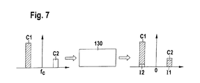
- Figure 7 illustrates the generation of the image signals 11, 12 during a conventional quadrature demodulation process.
- the multi-carrier signal as received via the antenna. It comprises for example a first carrier signal C1 and a second carrier signal C2 which are both free of image signals. These carrier signals are located at a first and a second mirror carrier frequency, respectively. These mirror carrier frequencies are arranged symmetrically around a center frequency f c .
- the carrier signals after the converting process as carried out by the quadrature demodulator. It can be seen that the down-converted first carrier signal C1 comprises an image signal I2 of the second carrier signal C2 and that said second carrier signal comprises an image signal I1 of the second carrier signal C2.
- image signals are undesired because they make a reconstruction of the desired carrier signal more difficult.
- the difficulty of reconstruction depends on the ratio of image signal to carrier signal which itself depends on the level of impairments in the realisation of the analog quadrature demodulator (gain, phase & quadrature mismatches) as well as similar defects in the A to D converter chain.
- the traditional direct conversion receiver DCR further comprises an analog/digital converter for digitizing the down-converted multi-carrier signal and at least a first and a second down-converter DDC-unit for separating the first and the second carrier signal from the digitized down-converted multi-carrier signal and for translating the separated first and second carrier signal to be centered at a predetermined frequency in the frequency plane.
- said predetermined frequency is set to 0.
- this object is solved by the subject-matter of claim 1. More specifically, for the above-described direct conversion receiver this object is solved by providing an error estimating unit for calculating a compensating complex coefficient representing the quota and/or the phase position of the image signal of the second carrier signal being included in the first carrier signal and at least a first compensator stage for removing the undesired image signal from the first carrier signal in response to said compensating coefficient.
- the implementation of a such constructed direct conversion receiver is rather simple and allows an easy image rejection. It is another advantage of the invention that in all embodiments the compensating coefficient is at once calculated correctly so that a sufficient suppression of the image signals in the carrier signals is achieved and that a further processing of the carrier signal is possible; consequently, for most of the applications no further adaptation of said compensating coefficient, e. g. by carrying out further iterations, is required.
- direct' in direct conversion receiver means that A to D conversion is done directly in baseband representation of a complex analog signal as opposed to intermediate frequency sampling and digitizing method where the image problem does not exist but exibit much higher performance requirements for the A to D converter.
- the patent applies also to a superheterodyne receiver with a 1 st intermediate frequency band.
- the compensating coefficients are calculated from the translated down-converted carrier signals as output by the DDC-units and provided to compensator stages which are connected in series behind said DDC-units, respectively. Due to said open loop construction an iterative adaptation of the compensating coefficient is neither possible nor required because the accuracy of the calculated compensating coefficient is sufficient to achieve a proper removement of the image signals for most applications.
- the compensating coefficient is calculated in an iterative process in which the at least partially cleaned output signal of the direct conversion receiver are considered.
- the process for optimizing the compensating coefficients according to the invention is rather quick so that typically only one iteration loop has to be carried out for achieving a proper compensating coefficient which is already able to suppress the undesired image signals sufficiently and which allows a further processing of the carrier signals.
- these embodiments allow further iteration loops in which the compensating coefficient is further optimized.
- the above identified object is further solved by a method for receiving a multi-carrier signal and for rejecting undesired images within these carrier signals and by a computer program for carrying out said method. Moreover, the object is solved by an error estimating unit and by a compensator stage of a direct conversion receiver.
- the advantages of said solutions correspond to the advantages mentioned above with respect to the direct conversion receiver.
- Figure 1 shows a first embodiment of the direct conversion receiver DCR 100' according to the invention.
- Said DCR 100' serves for receiving a multi-carrier signal including at least a first and a second carrier signal - see spot S1 - being located at image carrier frequencies via an antenna 110.
- a front end 120 that can include itself some frequency band transposition the multi-carrier signal is directly down-converted to base band by a quadrature demodulator 130.
- the limited image rejection capabilities of said traditional quadrature demodulator 130 cause a superposition of the desired carrier signals and their images as described above by referring to Figure 7.
- This effect is further illustrated for a multi-carrier signal comprising four carrier signals C1, C2, C3 and C4 by the spots S1 and S2 shown in Figure 1.
- the images caused by the carrier signals C1 ... C4 are assigned by the reference numerals I1 ... I4, respectively.
- the inphase and quadrature components of the complex baseband are respectively digitized by analog/digital AD-converters 140.
- the carriers included in the multi-carrier base band signal are separated by digital down-converters DDCs 150-1 ... 150-4 which are individually provided for each of said carriers.
- DDCs 150-1 ... 150-4 which are individually provided for each of said carriers.
- the DDCs serve for translating the carrier signals in frequency to be centered at 0 Hz in the frequency plane.
- the image signal components I1 ... I4 are still present within the carrier signals C1 ... C4.
- each of the separated carriers C1 ... C4 is subsequently processed in an individually co-ordinated compensator stage 160'-1 ... 160'-4. More specifically, the translated first carrier signal output by the first DDC 150-1 is processed by the first compensator stage 160'-1.
- the same co-ordination applies to the other DDCs and compensator stages.
- the compensator stages 160'-1 ... 160'-4 remove the undesired image signals from the carrier signals in response to a provided compensating coefficient. Consequently, in the first embodiment according to Figure 1 each of said compensator stages 160'-1 ... 160'-4 outputs a cleaned carrier signal which is free of an undesired image signal component; this image rejection effect of the compensator stages is illustrated by the spots S3 and S4 in Figure 1.
- the compensator stages 160'-1 ... 160'-4 need information about the quota /magnitude and/or the phase of the undesired image signal component to be removed. This information is provided to the compensator stages by said compensating coefficients which are individually calculated by an error estimating unit 170 for each of said compensating stages.
- the compensating coefficients in the first embodiment are referred to as first type of compensating coefficients.
- the error estimating unit 170' of the first embodiment is embodied to calculate a first type compensating coefficient representing the amplitude/quota and/or the phase position the undesired image signal within the carrier signal to be cleaned. More specifically, according to Figure 1 it is assumed that the first carrier signal C1 includes an undesired image of the second carrier signal C2 and vice versa. Moreover, it is assumed that the third carrier signal C3 includes - after down-converting - an image 14 of the fourth carrier signal C4 and vice versa. Consequently, the first compensator stage 160-1 is embodied to reject the image 12 of the second carrier signal C2 from the first carrier signal C1. For achieving this, the first compensator stage 160'-1 receives both, the first and the second carrier signal as well as its individual compensating coefficient.
- the error estimating unit 170' in principle generates said compensating coefficients by correlating the output of the DDCs for the desired carrier signal with the DDC output of the image carrier. For example, for generating the individual compensating coefficient CC1 for the first compensator stage 160'-1 the error estimating unit 170' correlates the output of the first DDC 150-1 for the first carrier signal which shall be cleaned with the output of the second DDC 150-2, i. e. the translated second carrier signal, an image of which is included in the translated first carrier signal. From said complex compensating coefficient CC1 and from the levels of the two input signals, i. e. the translated down-converted first and second carrier signals the first compensator stage 160'-1 calculates the cleaned first carrier signal.
- the compensating coefficients only vary slow versus time. For this case it is sufficient to compute these compensating coefficients CCi with 1-4 from time to time.
- the compensating coefficients may be computed sequentially and offline with the result that only limited hardware and/or software resources are required.
- the compensator stages 160'-1 ... 160'-4 have to buffer a certain portion of their above-mentioned input signals in order to await the provision of the corresponding compensating coefficient from the error estimating unit 170'.
- the first compensating coefficient CC1 representing the amplitude/quota and/or the phase position of the image signal of the second carrier signal within the translated and down-converted first carrier signal is calculated.
- this compensating coefficient CC1 is provided to the first compensator stage 160'-1.
- said compensator stage 160'-1 the buffered input signals are processed by using said compensating coefficient CC1 in order to generate the desired clean first carrier signal.
- the term "clean" means a lack of image signals within a carrier signal. Due to its individual calculation the compensating coefficient CC1 it is highly accurate with the result that the undesired image signal components within the cleaned carrier signals are sufficiently suppressed for most applications; usually, no further adaptation of the compensating coefficient CC1 is necessary and thus the described method is best suited for fast varying scenarios.
- Figure 2 shows a second embodiment of the direct conversion receiver according to the present invention.
- the antenna 110, the front end 120, the quadrature demodulator 130, the analog/digital converters 140, the direct down-converters 150-1, 150-4 and the indirect compensator stages 160'-1 ... 160'-4 as well as the operations of said components are identical to the components being identified by the same reference numerals and operations thereof described above for the first embodiment.
- the second embodiment of the DCR according to Figure 2 differs from the first embodiment in that the input for the error estimating unit 170" is now taken from the output of the compensator stages 160'-1 ... 160'-4.
- the effect is that the error estimation operates in an iterative manner.
- said proposed iteration converges very fast so that normally only one iteration loop is sufficient for sufficiently suppressing the image signals.
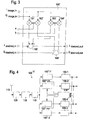
- Figure 3 shows a preferred embodiment of the indirect compensator stages 160'-1 ... 160'-4 as used in the first and second embodiment of the DCR in Figures 1 and 2, respectively.
- each of the compensator stages receives the real component I desired,in of the translated carrier signal to be cleaned.
- the imaginary component Q desired,in of the translated carrier signal to be cleaned is received.
- the compensator stages 160' further receive the real component I image,in of that translated carrier signal, an image of which is included in the translated carrier signal which is desired to be cleaned.
- the indirect compensator stage 160' receives the imaginary component Q image,in of the translated carrier signal an image of which is included in the translated carrier signal desired to be cleaned at the port.
- the indirect compensator stage 160 receives the real component a and the imaginary component b of the co-ordinated compensating coefficient.
- each of the compensator stages 160' comprise a first multiplying unit 161' for multiplying the imaginary component of the translated image carrier signal with a real component of the compensating coefficient a. Further, it comprises a second multiplying unit 162' for multiplying the real component of said translated image carrier signal I image,in with the real component a of the compensating coefficient. Moreover, it comprises a third multiplying unit 163' for multiplying the real component of the translated image carrier signal I image,in with the imaginary component b of the compensating coefficient and a fourth multiplying unit 164' for multiplying the imaginary component of the translated image carrier signal Q image,in with the imaginary component b of the compensating coefficient.
- each of the compensating stages comprise a first adding unit 165' for generating a real component of the desired cleaned carrier signal by adding the output of the third multiplying unit 163' to the real component of the translated carrier signal desired to be cleaned and by substracting the output of the first multiplying unit 161' therefrom.
- each of the compensator stages 160' comprises a second adding unit 166' for generating an imaginary component the of cleaned carrier signal by substracting the output of the second multiplying unit 162' and the output of the fourth multiplying unit 164' from the imaginary component of the translated carrier signal Q desired,in required to be cleaned.
- Figure 4 shows a third embodiment of the direct conversion receiver according to the invention.
- the operation of the antenna 110, the front end 120, the quadrature demodulator 130, the A/D-converter 140 and of the direct down-converters 150-1 ... 150-4 and the operations of these components are the same as described above.
- the third embodiment of the direct conversion receiver differs from the second embodiment substantially in that the compensator stages 160''-1 ... 160''-4 are now connected in series between the A/D-converter 140 and the digital down-converters 150-1.
- the digitized multi-carrier signal output by said A/D-converter 140 is now received by said compensator stages 160''-1 ... 160''-4 and these compensator stages output a cleaned multi-carrier signal; i. e. the output multi-carrier signal is substantially free of undesired image signals.
- the cleaned multi-carrier signals output by the compensator stages 160''-1 ... 160''-4 are received by the individually co-ordinated digital down-converters 150-1 ... 150-4 for separating individual carriers from said cleaned multi-carrier signal.
- the cleaning process carried out by the compensator stages is carried out here before the separation process is carried out by the DDCs.
- the compensating coefficients (third type) are now calculated in response to the output signal of the DDCs channels. In that way an individual adaptation of the compensating coefficient with regard to the carrier signal to be selected from the multi-carrier signal can be provided to said compensating stages 160''-1 ... 160''-4.
- the error estimating unit which is embodied to calculate these individual compensating coefficients is in embodiment 3 assigned by the reference numeral 170'''.
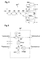
- Figure 5 shows a fourth embodiment of the claimed direct conversion receiver DCR.
- the construction of that fourth embodiment only differs from the third embodiment in that it is facilitated in the way that the plurality of compensator stages used in the third embodiment is here replaced by only one single compensating stage 160''. Due to that facilitation the error estimator unit 170 IV now generates only one fourth-type compensating coefficient for said single compensator stage 160'' in response to the individual signals output by said digital down-converters 150-1 ... 150-4. Because now there is only one compensating coefficient provided to said single compensator stage said compensating coefficient is not individually adapted to each of the carrier signals included within the multi-carrier signal processed by said compensating stage and which are subsequently to be separated by said digital down-converters 150-1 ... 150-4.
- the rejection of undesired image signals within the signals output by said digital down-converters is only suboptimal in comparison to for example embodiment 3.
- the generation of the compensating coefficient is also done in the form of a closed loop. Consequently, also in embodiment 4 an arbitrary accuracy of the compensating coefficient may be achieved perhaps by carrying out the closed loop for some more times than in the other embodiments.
- FIG. 6 shows a preferred embodiment of the compensator stages 160''-1 ... 160''-4 or 160 " as used in embodiments 3 and 4.
- said compensator stage receives a real component I desired,multi-in and an imaginary component Q desired,multi-in as well as the magnitude k and the phase p of the compensating coefficient for the multi-carrier signal as generated by the error estimating unit 170 IV .
- a constant I2DC is substracted from the received real component I desired,multi-in .
- the compensator stage 160'' comprises a substracting unit 161''.
- Said first multiplier 163'' generates a first intermediate signal.
- the compensating stage 160'' comprises a second substracting unit 164'' for generating a second intermediate signal by adding the first intermediate signal to the imaginary component Q desired,multi-in of the received multi-carrier signal and by substracting a second constant Q2DC therefrom.
- the error estimating unit 170 I ... 170 IV serves - as outlined above - to estimate the unknown compensating coefficients, that means in particular the amplitude and the phase imbalance in case of direct error compensation as used in embodiments 3 and 4 or in the form of a complex scaling factor, that means in the form of real component and imaginary component in the case of an indirect error compensation as used or done in embodiments 1 and 2.
- error estimation is done by correlating the "frequency inverted" signal of the corresponding image channel with the signal of the desired channel.
- the scaled complex correlation coefficient is used to compute the scaling factor used for indirect compensation whereas the scaled correlation coefficient is used to compute the amplitude and the phase imbalance of the real and imaginary component of the demodulator.
- the number of DDCs and/or compensator stages preferably corresponds to the number of carriers comprised within the received multi-carrier signal.
- the numbers are not limited for any embodiment of the invention, even if some embodiments have only been described for two carriers in order to facilitate the illustration.
Landscapes
- Engineering & Computer Science (AREA)
- Computer Networks & Wireless Communication (AREA)
- Signal Processing (AREA)
- Power Engineering (AREA)
- Digital Transmission Methods That Use Modulated Carrier Waves (AREA)
- Superheterodyne Receivers (AREA)
- Circuits Of Receivers In General (AREA)
- Measuring Pulse, Heart Rate, Blood Pressure Or Blood Flow (AREA)
- Input Circuits Of Receivers And Coupling Of Receivers And Audio Equipment (AREA)
Priority Applications (5)
| Application Number | Priority Date | Filing Date | Title |
|---|---|---|---|
| EP02360380A EP1435687B1 (fr) | 2002-12-30 | 2002-12-30 | Recepteur à conversion directe |
| DE60206065T DE60206065T2 (de) | 2002-12-30 | 2002-12-30 | Direktmischempfänger |
| AT02360380T ATE304240T1 (de) | 2002-12-30 | 2002-12-30 | Direktmischempfänger |
| US10/701,636 US7292836B2 (en) | 2002-12-30 | 2003-11-06 | Direct conversion receiver |
| CNB2003101154850A CN100517986C (zh) | 2002-12-30 | 2003-11-26 | 直接转换接收机 |
Applications Claiming Priority (1)
| Application Number | Priority Date | Filing Date | Title |
|---|---|---|---|
| EP02360380A EP1435687B1 (fr) | 2002-12-30 | 2002-12-30 | Recepteur à conversion directe |
Publications (2)
| Publication Number | Publication Date |
|---|---|
| EP1435687A1 true EP1435687A1 (fr) | 2004-07-07 |
| EP1435687B1 EP1435687B1 (fr) | 2005-09-07 |
Family
ID=32479836
Family Applications (1)
| Application Number | Title | Priority Date | Filing Date |
|---|---|---|---|
| EP02360380A Expired - Lifetime EP1435687B1 (fr) | 2002-12-30 | 2002-12-30 | Recepteur à conversion directe |
Country Status (5)
| Country | Link |
|---|---|
| US (1) | US7292836B2 (fr) |
| EP (1) | EP1435687B1 (fr) |
| CN (1) | CN100517986C (fr) |
| AT (1) | ATE304240T1 (fr) |
| DE (1) | DE60206065T2 (fr) |
Cited By (2)
| Publication number | Priority date | Publication date | Assignee | Title |
|---|---|---|---|---|
| EP2290828A3 (fr) * | 2009-09-01 | 2011-08-24 | Electronics and Telecommunications Research Institute | Appareil et procédé de réception |
| WO2013165289A1 (fr) * | 2012-05-03 | 2013-11-07 | Telefonaktiebolaget L M Ericsson (Publ) | Appareil récepteur de radiocommunication et procédé correspondant |
Families Citing this family (10)
| Publication number | Priority date | Publication date | Assignee | Title |
|---|---|---|---|---|
| US7684778B1 (en) * | 2005-02-23 | 2010-03-23 | Marvell International Ltd. | Image cancellation in receivers |
| JP5354750B2 (ja) * | 2010-07-21 | 2013-11-27 | Kddi株式会社 | イメージ信号を除去するアンダーサンプリングを用いた受信機、プログラム及び方法 |
| CN102655487B (zh) * | 2011-03-01 | 2015-09-23 | 瑞昱半导体股份有限公司 | 补偿装置、补偿模块、补偿参数计算模块及其接收器 |
| US8787860B2 (en) | 2011-07-21 | 2014-07-22 | Marvell World Trade Ltd. | Image cancellation in receivers using dual adaptive filters |
| US9197279B2 (en) | 2013-03-15 | 2015-11-24 | Blackberry Limited | Estimation and reduction of second order distortion in real time |
| US8811538B1 (en) | 2013-03-15 | 2014-08-19 | Blackberry Limited | IQ error correction |
| EP2779510B1 (fr) | 2013-03-15 | 2018-10-31 | BlackBerry Limited | Pondération statistique et ajustement de variables d'état dans une radio |
| US8942656B2 (en) | 2013-03-15 | 2015-01-27 | Blackberry Limited | Reduction of second order distortion in real time |
| US8983486B2 (en) | 2013-03-15 | 2015-03-17 | Blackberry Limited | Statistical weighting and adjustment of state variables in a radio |
| WO2017070939A1 (fr) * | 2015-10-30 | 2017-05-04 | 富士通株式会社 | Appareil de modulation multi-porteuse et appareil, procédé et système de démodulation multi-porteuse |
Citations (3)
| Publication number | Priority date | Publication date | Assignee | Title |
|---|---|---|---|---|
| EP0984288A1 (fr) * | 1998-09-03 | 2000-03-08 | Sony/Tektronix Corporation | Séparateur IQ à large bande et son procédé de calibration |
| US20020097812A1 (en) * | 2000-12-01 | 2002-07-25 | John Wiss | In-phase and quadrature-phase rebalancer |
| EP1241779A2 (fr) * | 2001-03-07 | 2002-09-18 | Nokia Corporation | Récepteur à multiples porteuses |
Family Cites Families (5)
| Publication number | Priority date | Publication date | Assignee | Title |
|---|---|---|---|---|
| IT1297278B1 (it) * | 1997-09-15 | 1999-08-09 | Italtel Spa | Radioricevitore digitale a larga banda per segnale multiportante |
| US6748200B1 (en) * | 2000-10-02 | 2004-06-08 | Mark A. Webster | Automatic gain control system and method for a ZIF architecture |
| US6694131B1 (en) * | 2001-02-21 | 2004-02-17 | Mitsubishi Electric Corporation | Method and apparatus for adaptive image rejection |
| WO2002084859A1 (fr) * | 2001-04-18 | 2002-10-24 | Nokia Corporation | Agencement de circuit equilibre et procede de linearisation de cet agencement |
| US7020226B1 (en) * | 2002-04-04 | 2006-03-28 | Nortel Networks Limited | I/Q distortion compensation for the reception of OFDM signals |
-
2002
- 2002-12-30 EP EP02360380A patent/EP1435687B1/fr not_active Expired - Lifetime
- 2002-12-30 DE DE60206065T patent/DE60206065T2/de not_active Expired - Lifetime
- 2002-12-30 AT AT02360380T patent/ATE304240T1/de not_active IP Right Cessation
-
2003
- 2003-11-06 US US10/701,636 patent/US7292836B2/en not_active Expired - Fee Related
- 2003-11-26 CN CNB2003101154850A patent/CN100517986C/zh not_active Expired - Fee Related
Patent Citations (3)
| Publication number | Priority date | Publication date | Assignee | Title |
|---|---|---|---|---|
| EP0984288A1 (fr) * | 1998-09-03 | 2000-03-08 | Sony/Tektronix Corporation | Séparateur IQ à large bande et son procédé de calibration |
| US20020097812A1 (en) * | 2000-12-01 | 2002-07-25 | John Wiss | In-phase and quadrature-phase rebalancer |
| EP1241779A2 (fr) * | 2001-03-07 | 2002-09-18 | Nokia Corporation | Récepteur à multiples porteuses |
Non-Patent Citations (4)
| Title |
|---|
| M. VALKAMA ET AL.: "Advanced DSP for I/Q imbalance compensation in a low-IF receiver", IEEE INTERNATIONAL CONFERENCE ON COMMUNICATIONS, vol. 2, 2000, pages 768 - 772, XP002240825 * |
| M. VALKAMA ET AL.: "Advanced methods for I/Q imbalance compensation in communication receivers", IEEE TRANSACTIONS ON SIGNAL PROCESSING, vol. 49, no. 10, October 2001 (2001-10-01), pages 2335 - 2344, XP002240824 * |
| SCHUCHERT A ET AL: "A novel IQ imbalance compensation scheme for the reception of OFDM signals", IEEE TRANSACTIONS ON CONSUMER ELECTRONICS, IEEE INC. NEW YORK, US, vol. 47, no. 3, August 2001 (2001-08-01), pages 313 - 318, XP002217600, ISSN: 0098-3063 * |
| VALKAMA ET AL.: "On the performance of interference canceller based I/Q imbalance compensation", PROCEEDINGS OF ICASSP 2000, vol. 5, 5 June 2000 (2000-06-05), pages 2885 - 2888, XP010506610 * |
Cited By (4)
| Publication number | Priority date | Publication date | Assignee | Title |
|---|---|---|---|---|
| EP2290828A3 (fr) * | 2009-09-01 | 2011-08-24 | Electronics and Telecommunications Research Institute | Appareil et procédé de réception |
| US8462884B2 (en) | 2009-09-01 | 2013-06-11 | Electronics And Telecommunications Research Institute | Receiving apparatus and receiving method |
| WO2013165289A1 (fr) * | 2012-05-03 | 2013-11-07 | Telefonaktiebolaget L M Ericsson (Publ) | Appareil récepteur de radiocommunication et procédé correspondant |
| US9692393B2 (en) | 2012-05-03 | 2017-06-27 | Telefonaktiebolaget Lm Ericsson (Publ) | Radio communication receiver apparatus and method |
Also Published As
| Publication number | Publication date |
|---|---|
| EP1435687B1 (fr) | 2005-09-07 |
| CN100517986C (zh) | 2009-07-22 |
| US7292836B2 (en) | 2007-11-06 |
| CN1512674A (zh) | 2004-07-14 |
| DE60206065T2 (de) | 2006-02-23 |
| ATE304240T1 (de) | 2005-09-15 |
| DE60206065D1 (de) | 2005-10-13 |
| US20040127188A1 (en) | 2004-07-01 |
Similar Documents
| Publication | Publication Date | Title |
|---|---|---|
| US6987815B2 (en) | Receive method and receiver in communication system | |
| JP3228353B2 (ja) | 適応位相制御付き復調方法及び装置 | |
| EP2060081B1 (fr) | Estimation d'un déséquilibre I/Q dépendant de la fréquence | |
| US20060183453A1 (en) | Methods and apparatus to perform signal removal in a low intermediate frequency receiver | |
| EP1435687A1 (fr) | Recepteur à conversion directe | |
| JPH0257373B2 (fr) | ||
| US7986930B2 (en) | IQ imbalance image suppression in presence of unknown phase shift | |
| KR20100102713A (ko) | 수신기의 2차 상호변조 보정 시스템 및 방법 | |
| EP3096500B1 (fr) | Appareil de communication, appareil de démodulation, appareil de reproduction de porteuse, appareil de compensation d'erreur de phase, procédé de compensation d'erreur de phase, et support d'informations sur lequel est stocké un programme de compensation d'erreur de phase | |
| US20120177151A1 (en) | Apparatus and method for adaptive i/q imbalance compensation | |
| US8798125B2 (en) | Phase tracking in communications systems | |
| CN116232558B (zh) | 一种iq时延补偿方法、装置、电子设备和存储介质 | |
| JP3549814B2 (ja) | 通信システムにおける受信方法及び受信機 | |
| JP5639777B2 (ja) | Dcオフセット補償システムおよび方法 | |
| JP2002199039A (ja) | 通信システムにおける受信方法及び受信機 | |
| JP3306736B2 (ja) | 周波数オフセット補償回路 | |
| JP2000049881A (ja) | 通信システム | |
| WO2012094087A1 (fr) | Appareil et procédé destinés à la compensation de déséquilibre i/q adaptatif | |
| KR100676568B1 (ko) | 타이밍추출장치 및 방법 그리고 그 타이밍추출장치를구비한 복조장치 | |
| KR100452619B1 (ko) | I/q부정합의 추정 및 보상방법과 그 장치, i/q부정합과 dc옵셋의 추정 및 보상방법과 그 장치 | |
| CN112532260B (zh) | 一种接收机iq失衡估计和补偿方法及装置 | |
| JP2956724B2 (ja) | オーバーサンプリングトランスバーサル等化器 | |
| EP1324529A2 (fr) | Méthode d'estimation d'horloge de symbole par une manière en avale | |
| JP2006166257A (ja) | タイミング同期回路 | |
| US8139627B2 (en) | DC offset estimation in received signals |
Legal Events
| Date | Code | Title | Description |
|---|---|---|---|
| PUAI | Public reference made under article 153(3) epc to a published international application that has entered the european phase |
Free format text: ORIGINAL CODE: 0009012 |
|
| 17P | Request for examination filed |
Effective date: 20030606 |
|
| AK | Designated contracting states |
Kind code of ref document: A1 Designated state(s): AT BE BG CH CY CZ DE DK EE ES FI FR GB GR IE IT LI LU MC NL PT SE SI SK TR |
|
| AX | Request for extension of the european patent |
Extension state: AL LT LV MK RO |
|
| GRAP | Despatch of communication of intention to grant a patent |
Free format text: ORIGINAL CODE: EPIDOSNIGR1 |
|
| AKX | Designation fees paid |
Designated state(s): AT BE BG CH CY CZ DE DK EE ES FI FR GB GR IE IT LI LU MC NL PT SE SI SK TR |
|
| GRAS | Grant fee paid |
Free format text: ORIGINAL CODE: EPIDOSNIGR3 |
|
| GRAA | (expected) grant |
Free format text: ORIGINAL CODE: 0009210 |
|
| AK | Designated contracting states |
Kind code of ref document: B1 Designated state(s): AT BE BG CH CY CZ DE DK EE ES FI FR GB GR IE IT LI LU MC NL PT SE SI SK TR |
|
| PG25 | Lapsed in a contracting state [announced via postgrant information from national office to epo] |
Ref country code: BE Free format text: LAPSE BECAUSE OF FAILURE TO SUBMIT A TRANSLATION OF THE DESCRIPTION OR TO PAY THE FEE WITHIN THE PRESCRIBED TIME-LIMIT Effective date: 20050907 Ref country code: CZ Free format text: LAPSE BECAUSE OF FAILURE TO SUBMIT A TRANSLATION OF THE DESCRIPTION OR TO PAY THE FEE WITHIN THE PRESCRIBED TIME-LIMIT Effective date: 20050907 Ref country code: CH Free format text: LAPSE BECAUSE OF FAILURE TO SUBMIT A TRANSLATION OF THE DESCRIPTION OR TO PAY THE FEE WITHIN THE PRESCRIBED TIME-LIMIT Effective date: 20050907 Ref country code: SK Free format text: LAPSE BECAUSE OF FAILURE TO SUBMIT A TRANSLATION OF THE DESCRIPTION OR TO PAY THE FEE WITHIN THE PRESCRIBED TIME-LIMIT Effective date: 20050907 Ref country code: FI Free format text: LAPSE BECAUSE OF FAILURE TO SUBMIT A TRANSLATION OF THE DESCRIPTION OR TO PAY THE FEE WITHIN THE PRESCRIBED TIME-LIMIT Effective date: 20050907 Ref country code: AT Free format text: LAPSE BECAUSE OF FAILURE TO SUBMIT A TRANSLATION OF THE DESCRIPTION OR TO PAY THE FEE WITHIN THE PRESCRIBED TIME-LIMIT Effective date: 20050907 Ref country code: NL Free format text: LAPSE BECAUSE OF FAILURE TO SUBMIT A TRANSLATION OF THE DESCRIPTION OR TO PAY THE FEE WITHIN THE PRESCRIBED TIME-LIMIT Effective date: 20050907 Ref country code: LI Free format text: LAPSE BECAUSE OF FAILURE TO SUBMIT A TRANSLATION OF THE DESCRIPTION OR TO PAY THE FEE WITHIN THE PRESCRIBED TIME-LIMIT Effective date: 20050907 Ref country code: EE Free format text: LAPSE BECAUSE OF FAILURE TO SUBMIT A TRANSLATION OF THE DESCRIPTION OR TO PAY THE FEE WITHIN THE PRESCRIBED TIME-LIMIT Effective date: 20050907 Ref country code: SI Free format text: LAPSE BECAUSE OF FAILURE TO SUBMIT A TRANSLATION OF THE DESCRIPTION OR TO PAY THE FEE WITHIN THE PRESCRIBED TIME-LIMIT Effective date: 20050907 Ref country code: TR Free format text: LAPSE BECAUSE OF FAILURE TO SUBMIT A TRANSLATION OF THE DESCRIPTION OR TO PAY THE FEE WITHIN THE PRESCRIBED TIME-LIMIT Effective date: 20050907 |
|
| REG | Reference to a national code |
Ref country code: GB Ref legal event code: FG4D |
|
| REG | Reference to a national code |
Ref country code: CH Ref legal event code: EP |
|
| REG | Reference to a national code |
Ref country code: IE Ref legal event code: FG4D |
|
| REF | Corresponds to: |
Ref document number: 60206065 Country of ref document: DE Date of ref document: 20051013 Kind code of ref document: P |
|
| PG25 | Lapsed in a contracting state [announced via postgrant information from national office to epo] |
Ref country code: GR Free format text: LAPSE BECAUSE OF FAILURE TO SUBMIT A TRANSLATION OF THE DESCRIPTION OR TO PAY THE FEE WITHIN THE PRESCRIBED TIME-LIMIT Effective date: 20051207 Ref country code: BG Free format text: LAPSE BECAUSE OF FAILURE TO SUBMIT A TRANSLATION OF THE DESCRIPTION OR TO PAY THE FEE WITHIN THE PRESCRIBED TIME-LIMIT Effective date: 20051207 Ref country code: DK Free format text: LAPSE BECAUSE OF FAILURE TO SUBMIT A TRANSLATION OF THE DESCRIPTION OR TO PAY THE FEE WITHIN THE PRESCRIBED TIME-LIMIT Effective date: 20051207 Ref country code: SE Free format text: LAPSE BECAUSE OF FAILURE TO SUBMIT A TRANSLATION OF THE DESCRIPTION OR TO PAY THE FEE WITHIN THE PRESCRIBED TIME-LIMIT Effective date: 20051207 |
|
| PG25 | Lapsed in a contracting state [announced via postgrant information from national office to epo] |
Ref country code: ES Free format text: LAPSE BECAUSE OF FAILURE TO SUBMIT A TRANSLATION OF THE DESCRIPTION OR TO PAY THE FEE WITHIN THE PRESCRIBED TIME-LIMIT Effective date: 20051218 |
|
| PG25 | Lapsed in a contracting state [announced via postgrant information from national office to epo] |
Ref country code: CY Free format text: LAPSE BECAUSE OF FAILURE TO SUBMIT A TRANSLATION OF THE DESCRIPTION OR TO PAY THE FEE WITHIN THE PRESCRIBED TIME-LIMIT Effective date: 20051230 Ref country code: IE Free format text: LAPSE BECAUSE OF NON-PAYMENT OF DUE FEES Effective date: 20051230 |
|
| PG25 | Lapsed in a contracting state [announced via postgrant information from national office to epo] |
Ref country code: MC Free format text: LAPSE BECAUSE OF NON-PAYMENT OF DUE FEES Effective date: 20051231 Ref country code: LU Free format text: LAPSE BECAUSE OF NON-PAYMENT OF DUE FEES Effective date: 20051231 |
|
| PG25 | Lapsed in a contracting state [announced via postgrant information from national office to epo] |
Ref country code: PT Free format text: LAPSE BECAUSE OF FAILURE TO SUBMIT A TRANSLATION OF THE DESCRIPTION OR TO PAY THE FEE WITHIN THE PRESCRIBED TIME-LIMIT Effective date: 20060207 |
|
| NLV1 | Nl: lapsed or annulled due to failure to fulfill the requirements of art. 29p and 29m of the patents act | ||
| REG | Reference to a national code |
Ref country code: CH Ref legal event code: PL |
|
| ET | Fr: translation filed | ||
| PLBE | No opposition filed within time limit |
Free format text: ORIGINAL CODE: 0009261 |
|
| STAA | Information on the status of an ep patent application or granted ep patent |
Free format text: STATUS: NO OPPOSITION FILED WITHIN TIME LIMIT |
|
| 26N | No opposition filed |
Effective date: 20060608 |
|
| REG | Reference to a national code |
Ref country code: IE Ref legal event code: MM4A |
|
| PGFP | Annual fee paid to national office [announced via postgrant information from national office to epo] |
Ref country code: IT Payment date: 20101227 Year of fee payment: 9 |
|
| PG25 | Lapsed in a contracting state [announced via postgrant information from national office to epo] |
Ref country code: IT Free format text: LAPSE BECAUSE OF NON-PAYMENT OF DUE FEES Effective date: 20111230 |
|
| REG | Reference to a national code |
Ref country code: FR Ref legal event code: CA Effective date: 20130612 Ref country code: FR Ref legal event code: TP Owner name: ALCATEL LUCENT, FR Effective date: 20130612 |
|
| REG | Reference to a national code |
Ref country code: FR Ref legal event code: GC Effective date: 20130920 |
|
| REG | Reference to a national code |
Ref country code: FR Ref legal event code: RG Effective date: 20141016 |
|
| PGFP | Annual fee paid to national office [announced via postgrant information from national office to epo] |
Ref country code: DE Payment date: 20141211 Year of fee payment: 13 Ref country code: GB Payment date: 20141219 Year of fee payment: 13 |
|
| PGFP | Annual fee paid to national office [announced via postgrant information from national office to epo] |
Ref country code: FR Payment date: 20141219 Year of fee payment: 13 |
|
| REG | Reference to a national code |
Ref country code: DE Ref legal event code: R119 Ref document number: 60206065 Country of ref document: DE |
|
| GBPC | Gb: european patent ceased through non-payment of renewal fee |
Effective date: 20151230 |
|
| REG | Reference to a national code |
Ref country code: FR Ref legal event code: ST Effective date: 20160831 |
|
| PG25 | Lapsed in a contracting state [announced via postgrant information from national office to epo] |
Ref country code: GB Free format text: LAPSE BECAUSE OF NON-PAYMENT OF DUE FEES Effective date: 20151230 Ref country code: DE Free format text: LAPSE BECAUSE OF NON-PAYMENT OF DUE FEES Effective date: 20160701 |
|
| PG25 | Lapsed in a contracting state [announced via postgrant information from national office to epo] |
Ref country code: FR Free format text: LAPSE BECAUSE OF NON-PAYMENT OF DUE FEES Effective date: 20151231 |