EP1436765B1 - Adaptateur pour la mise en contact de cartes a puce - Google Patents
Adaptateur pour la mise en contact de cartes a puce Download PDFInfo
- Publication number
- EP1436765B1 EP1436765B1 EP02801891A EP02801891A EP1436765B1 EP 1436765 B1 EP1436765 B1 EP 1436765B1 EP 02801891 A EP02801891 A EP 02801891A EP 02801891 A EP02801891 A EP 02801891A EP 1436765 B1 EP1436765 B1 EP 1436765B1
- Authority
- EP
- European Patent Office
- Prior art keywords
- circuit board
- adapter
- elements
- receiving channel
- spring elements
- Prior art date
- Legal status (The legal status is an assumption and is not a legal conclusion. Google has not performed a legal analysis and makes no representation as to the accuracy of the status listed.)
- Expired - Lifetime
Links
Images


Classifications
-
- G—PHYSICS
- G06—COMPUTING OR CALCULATING; COUNTING
- G06K—GRAPHICAL DATA READING; PRESENTATION OF DATA; RECORD CARRIERS; HANDLING RECORD CARRIERS
- G06K19/00—Record carriers for use with machines and with at least a part designed to carry digital markings
- G06K19/06—Record carriers for use with machines and with at least a part designed to carry digital markings characterised by the kind of the digital marking, e.g. shape, nature, code
- G06K19/067—Record carriers with conductive marks, printed circuits or semiconductor circuit elements, e.g. credit or identity cards also with resonating or responding marks without active components
- G06K19/07—Record carriers with conductive marks, printed circuits or semiconductor circuit elements, e.g. credit or identity cards also with resonating or responding marks without active components with integrated circuit chips
- G06K19/077—Constructional details, e.g. mounting of circuits in the carrier
- G06K19/07737—Constructional details, e.g. mounting of circuits in the carrier the record carrier consisting of two or more mechanically separable parts
- G06K19/07741—Constructional details, e.g. mounting of circuits in the carrier the record carrier consisting of two or more mechanically separable parts comprising a first part operating as a regular record carrier and a second attachable part that changes the functional appearance of said record carrier, e.g. a contact-based smart card with an adapter part which, when attached to the contact card makes the contact card function as a non-contact card
-
- G—PHYSICS
- G06—COMPUTING OR CALCULATING; COUNTING
- G06K—GRAPHICAL DATA READING; PRESENTATION OF DATA; RECORD CARRIERS; HANDLING RECORD CARRIERS
- G06K7/00—Methods or arrangements for sensing record carriers, e.g. for reading patterns
- G06K7/0013—Methods or arrangements for sensing record carriers, e.g. for reading patterns by galvanic contacts, e.g. card connectors for ISO-7816 compliant smart cards or memory cards, e.g. SD card readers
- G06K7/0047—Methods or arrangements for sensing record carriers, e.g. for reading patterns by galvanic contacts, e.g. card connectors for ISO-7816 compliant smart cards or memory cards, e.g. SD card readers for reading/sensing record carriers having edge contacts
-
- H—ELECTRICITY
- H01—ELECTRIC ELEMENTS
- H01R—ELECTRICALLY-CONDUCTIVE CONNECTIONS; STRUCTURAL ASSOCIATIONS OF A PLURALITY OF MUTUALLY-INSULATED ELECTRICAL CONNECTING ELEMENTS; COUPLING DEVICES; CURRENT COLLECTORS
- H01R13/00—Details of coupling devices of the kinds covered by groups H01R12/70 or H01R24/00 - H01R33/00
- H01R13/02—Contact members
- H01R13/22—Contacts for co-operating by abutting
- H01R13/24—Contacts for co-operating by abutting resilient; resiliently-mounted
-
- H—ELECTRICITY
- H01—ELECTRIC ELEMENTS
- H01R—ELECTRICALLY-CONDUCTIVE CONNECTIONS; STRUCTURAL ASSOCIATIONS OF A PLURALITY OF MUTUALLY-INSULATED ELECTRICAL CONNECTING ELEMENTS; COUPLING DEVICES; CURRENT COLLECTORS
- H01R2201/00—Connectors or connections adapted for particular applications
- H01R2201/06—Connectors or connections adapted for particular applications for computer periphery
Definitions
- the invention relates to an adapter for contacting smart cards, in particular with a standardized according to the PCMCIA standard connection of a data processing device, with a card-shaped housing, which opens at one end into a receiving channel insertion slot for receiving a smart card and arranged on the opposite end Having terminal array, and with an electrically connected to the pad circuit board, which extends parallel to the receiving channel and is provided with contact elements for contacting the chip card.
- a chip card designed as a contact reader units which allow in the form of an adapter system, for example, a Chip card to connect to a standard PCMCIA standard connection of a data processing system.
- the known in the art for this purpose adapters have a PCMCIA plug-in socket, which causes a mechanical and electrical contact with a PCMCIA slot of the data processing system.
- the read-out of the chip card takes place via arranged in the receiving channel for the chip card contact elements which contact the same touching or, for example, on optical or magnetic way, without contact.
- An adapter for contacting chip cards is known, for example, from US Pat. No. 6,272,017 B1.
- the adapter has a card-shaped housing with an opening on a front side opening into a receiving channel slot for receiving a smart card and a arranged on the opposite end side panel.
- a printed circuit board is electrically connected, which extends parallel to the receiving channel and is provided with contact elements for contacting the chip card.
- a contacting unit for card-shaped carrier elements of electronic assemblies comprising a base plate with a plane-parallel recording of a card-shaped support member suitable size, at least one arranged substantially parallel to the base plate circuit board with contact elements for the electronic components of the support element its surface and is provided with a arranged at one edge of the base plate connection panel.
- a to the base plate substantially congruent, plate-shaped cover member forms with the circuit board a slot-like insertion channel and is attached to the base plate in the region of the connection pad and the opposite corners. Due to the mounting in the housing, the printed circuit board fills the full installation space in the housing.
- the invention has for its object to provide an adapter for contacting smart cards, in particular with a standard PCMCIA standard connection of a data processing device or the like, the above mentioned type, to the effect that the economic benefits of higher component integration can be used by the PCB manufacturing, so that a simple and cost-effective production can be achieved, which ensures an economical mass production, especially in view of the increasingly extensive use of prescribed card systems.
- the circuit board in the extension direction of the receiving channel has a relation to the receiving channel shortened length and the insertion slot facing end side with a device for positioning the circuit board and for guiding the chip card in the receiving channel is provided.
- the invention which is defined in the claims, is based on the recognition that the printed circuit board surface must be reduced in order to take advantage of the economic advantages of higher component integration. This reduction not only brings savings in PCB base material, but also benefits in PCB manufacturing.
- the device according to the invention for positioning the printed circuit board and for guiding the chip card in the receiving channel simultaneously ensures reliable contacting of a chip card inserted into the receiving channel, so that the two cost advantages, the saving of printed circuit board base material on the one hand and the increase in benefits in printed circuit board production on the other hand, are usable.
- Such a ausgestalteter adapter can be easily and inexpensively manufactured and therefore allows a mass production in the aforementioned sense. This is due to the fact that the advantageously the circuit board floating einklemmende means for a secure positioning of the shortened circuit board in the receiving channel of the housing of the adapter and on the other a secure guidance and contacting the chip card in the receiving channel of the housing of the adapter between the circuit board and the upper cover plate ensured the housing of the adapter.
- the plug-card-shaped housing on one end face has a slot for receiving a memory card and on the opposite end face a pad which is electrically connected to a printed circuit board arranged in the housing.
- the circuit board is in the known adapter shorter than the overall length of the housing, but the memory card is not - as in the invention - pushed over or under the circuit board, so that the contact fields of the memory card and the circuit board face each other, but the receiving channel of the housing is arranged such that the memory card to be read out is brought to the end of the circuit board and contacted via contact pins also on the front side.
- the device for positioning the printed circuit board arm-shaped support members and arm-shaped spring elements with a fixed end and a free end, wherein the free ends of the support members and the spring elements on opposite sides of the circuit board extending in the direction of the pad.
- the arm-shaped support elements and spring elements thus provide functional elements for the chip card guide and the printed circuit board receptacle.
- the circuit board is clamped floating between the arm-shaped support members and the arm-shaped spring elements. Characterized in that the device is connected directly to the circuit board, the PCB length is variable depending on the application without changes to the housing of the adapter or the receiving channel.
- PCMCIA adapter instead of usual for PCMCIA adapter
- the arm-shaped spring elements cam-shaped locking means, which engage in corresponding thereto provided on the sides of the circuit board receptacles.
- the cam-shaped latching means are advantageously arranged at the free end of the spring element and the receptacles are holes formed in the printed circuit board, preferably catching holes, or recesses formed in the printed circuit board.
- the locking means ensure a secure connection between the circuit board and the device.
- the spring elements guide and / or abutment means for positioning the circuit board on the device are formed as arranged on the spring elements tabs which are aligned with the longitudinal sides of the circuit board.
- the device has two support elements and two spring elements, which extend in the extension direction of the receiving channel parallel to and at a distance from each other and perpendicular to the extension direction of the receiving channel from each other.
- the support elements and the spring elements are arranged symmetrically to the front side, preferably such that the spring elements are outside and the support elements inside, particularly preferably such that the support elements are positioned to the left and right of the contact elements of the circuit board.
- the arms of the spring elements in the extension direction of the receiving channel on a serving for guiding the chip card projection.
- the device for further guidance of the chip card arm-shaped spring elements which extend in the direction of the pad and are placed over the circuit board to the contact elements.
- the device of the further between the spring elements preferably in the center of the end face of the Printed circuit board, extending in the direction of the pad field ramp-shaped projection which extends on the side opposite the support elements of the circuit board to the contact elements of the circuit board.
- the ramp-shaped projection advantageously leads with respect to a contact contact with the chip card when guiding the chip card of the projection of the latching means having spring elements.
- a further embodiment .der invention provides that the advantageously made of plastic device is integrally formed, preferably as a plastic injection molded part.
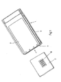
- the adapter 1 shown in Figure 1 has a housing whose dimensions correspond to those of a type II PCMCIA card.
- the housing 3 of the adapter 1 is provided on the right in Figure 1 located on the front side with a PCMCIA connection pad 8, which as seen in Figure 2 - completely housed in the housing 3.
- the housing 3 has at the terminal box 8 opposite end face an insertion slot 7 for a smart card 2, which merges into a laterally open receiving channel 6.
- the chip card 2 is provided with a flat contact field 18 and can be inserted or pulled out in the direction of the double arrow shown in the housing 3 of the adapter 1.
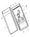
- the housing 3 of the adapter 1 consists of an upper cover plate 4 and a lower cover plate 5, which are connected to one another by a frame-shaped intermediate element 19.
- the cover plates 4 and 5 produced as stamped sheet metal parts have orthogonally angled staples 20 and 21, which ensures a simple but nevertheless reliable connection of the cover plates 4 and 5 with the intermediate element 19, which can be designed in several parts, despite different materials.
- That at the arranged lower cover plate intermediate member 19 is formed as a substantially U-shaped frame, whose legs on its inner contour clamping and guiding portions for receiving the circuit board 9 and the device 11 have.
- the intermediate element 19 in the region of the insertion slot 7 on an end face inlet bevel 22, which allows easy insertion of the smart card 2 in the receiving channel 6 of the adapter. Due to the frame-like configuration of the intermediate element 19, a high connection rigidity of the housing 3 of the adapter 1 is ensured.
- the circuit board 9 has a shortened in the extension direction of the receiving channel 6 relative to the receiving channel 6 length and is provided on the insertion slot 7 facing end with a device 11 for positioning the circuit board 9 and for guiding the smart card 2 in the receiving channel 6, wherein the device
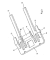
- the plastic-made device 11 for positioning the printed circuit board 9 has two arm-shaped support elements 12 and two arm-shaped spring elements 13 with a fixed end and a free end which extends in the extension direction of the Receiving channels 6 extend parallel and perpendicular to the extension direction of the receiving channel 6 are spaced from each other.
- the free ends of the support members 12 and the spring elements 13 extend on opposite sides of the circuit board 9 in the direction of the pad 8, which is electrically and mechanically connected to the circuit board 9 via contact elements 23. Due to the floating reception of the printed circuit board 9 via the device 11, the printed circuit board length can be designed variably. By varying the thickness of the support members 12 in the extension direction of the receiving channel a height adjustment for positioning the circuit board in the receiving channel 6 is given, so that an adaptation to different thickness boards with the device 11 for positioning in the receiving channel 6 of the adapter 1 is given.
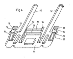
- the spring elements 13, as shown in Figures 4 and 7, in the region of its free end cams 14, which engage in corresponding holes of the shortened circuit board 9, as shown in Figure 9 can be seen.
- the spring elements 13 for positioning the circuit board strap-like guide means 15 which are aligned with the longitudinal sides of the circuit board 9, as can be seen in particular with reference to Figure 9.
- the in length compared to the Receiving channel 6 shortened circuit board 9 is clamped floating between the symmetrical to the front side parent support elements 12 and spring elements 13, wherein the support members 12 come to lie on the one and the spring elements 13 on the opposite side of the circuit board 9, as with reference to the figures 8, 9 and 10 to recognize.
- the spring elements 13 are positioned on the left and right of the contact elements 10 for contacting the contact pad 18 of a chip card 2.
- the so floating between the support members 12 and provided with cams 14 as locking means spring elements 13 floating mounted circuit board can compensate with the help of the device 11 position tolerances within the circuit board recording.
- the device 11 has to guide the chip card 2 arm-shaped spring elements 16 which extend in the direction of the pad 8 on the support elements 12 opposite side and are placed over the circuit board 9 to the contact elements 10, as shown in Figure 8 and 10 ,
- the spring elements 16 are arranged symmetrically to the front side of the circuit board.
- the ramp-like projection 17 and the projection 24 of the spring elements 13 are matched with respect to a touch contact with the smart card 2 in the leadership of the smart card 2 when inserting the smart card 2 in the receiving channel 6 such that the ramp-like projection 17 of the projection 24 of the spring elements 13 lags ,
- the projection 24 of the spring elements 13 in turn is formed lagging with respect to a touch contact with the chip card 2 of the establishment of the spring elements 16.
- the projection 17 and the spring elements 15 have a contact surface 25 or 26 for the front side of the printed circuit board 9, which serve for defined positioning of the printed circuit board 9 on the device 11.
Landscapes
- Engineering & Computer Science (AREA)
- Physics & Mathematics (AREA)
- General Physics & Mathematics (AREA)
- Theoretical Computer Science (AREA)
- Computer Hardware Design (AREA)
- Microelectronics & Electronic Packaging (AREA)
- Artificial Intelligence (AREA)
- Computer Vision & Pattern Recognition (AREA)
- Coupling Device And Connection With Printed Circuit (AREA)
- Details Of Connecting Devices For Male And Female Coupling (AREA)
Claims (16)
- Adaptateur (1) pour la mise en contact de cartes à puce (2), avec- un boîtier (3) en forme de carte à insérer, qui possède sur une face d'extrémité une fente d'insertion (7) débouchant dans un canal de réception (6) pour recevoir une carte à puce (2) ainsi qu'un champ de connexion (8) disposé sur la face d'extrémité opposée, et avec- une carte de circuits (9) connectée électriquement au champ de connexion (8), qui s'étend parallèlement au canal de réception (6) et qui est pourvue d'éléments de contact (10) pour la mise en contact de la carte à puce (2),caractérisé en ce que la carte de circuits (9) est plus courte que le canal de réception (6) dans le sens de l'étendue du canal de réception (6) et possède sur sa face d'extrémité tournée vers la fente d'insertion (7) un dispositif (11) pour positionner la carte de circuits (9) et pour guider la carte à puce (2) dans le canal de réception (6).
- Adaptateur selon la revendication 1, caractérisé en ce que le dispositif (11) serre la carte de circuits (9) avec un jeu.
- Adaptateur selon la revendication 1 ou la revendication 2, caractérisé en ce que le dispositif (11) pour positionner la carte de circuits (9) possède des éléments portants (12) en forme de bras et des éléments élastiques (13) en forme de bras avec une extrémité fixe et une extrémité libre, les extrémités libres des éléments portants (12) et des éléments élastiques (13) s'étendant en direction du champ de connexion (8) sur des faces opposées de la carte de circuits (9).
- Adaptateur selon la revendication 3, caractérisé en ce que les éléments élastiques (13) présentent des moyens d'engagement (14) en forme de cames, qui se mettent en prise dans des réceptacles correspondants sur la carte de circuits (9).
- Adaptateur selon la revendication 4, caractérisé en ce que les moyens d'engagement (14) sont disposés à l'extrémité libre de l'élément élastique (13).
- Adaptateur selon la revendication 4 ou 5, caractérisé en ce que les réceptacles sont des trous formés dans la carte de circuits (9), de préférence des trous de positionnement.
- Adaptateur selon la revendication 4 ou 5, caractérisé en ce que les réceptacles sont des renfoncements formés dans la carte de circuits (9).
- Adaptateur selon l'une quelconque des revendications 3 à 7, caractérisé en ce que les éléments élastiques (13) possèdent des moyens de guidage (15) pour positionner la carte de circuits (9) sur le dispositif (11).
- Adaptateur selon l'une quelconque des revendications 3 à 8, caractérisé en ce que le dispositif (11) possède deux éléments portants (12) et deux éléments élastiques (13), qui sont de préférence parallèles l'un à l'autre dans le sens de l'extension du canal de réception et distants l'un de l'autre et qui sont écartés l'un de l'autre perpendiculairement au sens de l'extension du canal de réception.
- Adaptateur selon la revendication 9, caractérisé en ce que les éléments portants (12) et les éléments élastiques (13) sont disposés de façon symétrique par rapport à la face d'extrémité, de préférence de telle manière que les éléments élastiques (13) se trouvent sur l'extérieur et les éléments portants (12) sur l'intérieur, et notamment de telle manière que les éléments portants (12) puissent être positionnés à gauche et à droite des éléments de contact (10) de la carte de circuits (9).
- Adaptateur selon l'une quelconque des revendications 3 à 10, caractérisé en ce que le bras des éléments élastiques (13) possède dans le sens de l'extension du canal de réception une échancrure (24) servant au guidage de la carte à puce (2).
- Adaptateur selon l'une quelconque des revendications 1 à 11, caractérisé en ce que le dispositif (11) pour le guidage de la carte à puce (2) possède des éléments élastiques en forme de bras (16), qui s'étendent en direction du champ de connexion (8) et sont posés sur la carte de circuits (9) jusqu'aux éléments de contact (10).
- Adaptateur selon la revendication 12, caractérisé en ce que le dispositif (11) présente entre les éléments élastiques (16), de préférence au milieu de la face d'extrémité de la carte de circuits (9), une saillie en forme de rampe (17) s'étendant en direction du champ de connexion (8), qui s'étend du côté de la carte de circuits (9) faisant face aux éléments portants (12) jusqu'aux éléments de contact (10) de la carte de circuits (9).
- Adaptateur selon la revendication 13, caractérisé en ce que la saillie en forme de rampe (17) suit l'échancrure (24) et la disposition des éléments élastiques (16) lors du guidage de la carte à puce (2) en vue d'un contact avec la carte à puce (2).
- Adaptateur selon l'une quelconque des revendications 1 à 14, caractérisé en ce que le dispositif (11) est formé d'un seul tenant.
- Adaptateur selon l'une quelconque des revendications 1 à 15, caractérisé en ce que le dispositif (11) est fait de plastique, de préférence d'une pièce en plastique moulé par injection.
Applications Claiming Priority (3)
| Application Number | Priority Date | Filing Date | Title |
|---|---|---|---|
| DE20117188U DE20117188U1 (de) | 2001-10-19 | 2001-10-19 | Adapter zum Kontaktieren von Chipkarten |
| DE20117188U | 2001-10-19 | ||
| PCT/EP2002/011558 WO2003036551A1 (fr) | 2001-10-19 | 2002-10-16 | Adaptateur pour la mise en contact de cartes a puce |
Publications (2)
| Publication Number | Publication Date |
|---|---|
| EP1436765A1 EP1436765A1 (fr) | 2004-07-14 |
| EP1436765B1 true EP1436765B1 (fr) | 2006-11-15 |
Family
ID=7963064
Family Applications (1)
| Application Number | Title | Priority Date | Filing Date |
|---|---|---|---|
| EP02801891A Expired - Lifetime EP1436765B1 (fr) | 2001-10-19 | 2002-10-16 | Adaptateur pour la mise en contact de cartes a puce |
Country Status (7)
| Country | Link |
|---|---|
| US (1) | US6967848B2 (fr) |
| EP (1) | EP1436765B1 (fr) |
| JP (1) | JP2005506638A (fr) |
| AT (1) | ATE345541T1 (fr) |
| DE (2) | DE20117188U1 (fr) |
| NO (1) | NO20032646L (fr) |
| WO (1) | WO2003036551A1 (fr) |
Families Citing this family (8)
| Publication number | Priority date | Publication date | Assignee | Title |
|---|---|---|---|---|
| DE102004013320A1 (de) * | 2004-03-17 | 2005-09-29 | Giesecke & Devrient Gmbh | Vorrichtung zum Verbinden einer Smart Card mit einem USB-Anschluss |
| US7040905B1 (en) * | 2005-05-18 | 2006-05-09 | Epo Science & Technology Inc. | Structure for combining printing circuit board with rack |
| US7097511B1 (en) * | 2005-07-21 | 2006-08-29 | Research In Motion Limited | Structure for SIM card assembly and disassembly |
| DE102005061688A1 (de) * | 2005-12-21 | 2007-07-05 | Stocko Contact Gmbh & Co. Kg | Kontaktiereinheit |
| US8665603B2 (en) * | 2007-12-03 | 2014-03-04 | Osram Gesellschaft Mit Beschraenkter Haftung | Housing for electrical components |
| US9136621B1 (en) * | 2012-08-14 | 2015-09-15 | Ciena Corporation | Guides and tab arrangement to retain a card having an edge connector and method of use |
| JP2014085936A (ja) * | 2012-10-25 | 2014-05-12 | Toshiba Corp | 電子機器 |
| TWM459640U (zh) * | 2013-04-09 | 2013-08-11 | Chi Mei Comm Systems Inc | 晶片卡裝取結構及具有該晶片卡裝取結構之電子裝置 |
Citations (3)
| Publication number | Priority date | Publication date | Assignee | Title |
|---|---|---|---|---|
| DE3902230A1 (de) * | 1989-01-26 | 1990-08-02 | Daimler Benz Ag | Einrichtung zur befestigung eines elektrischen moduls an einem basisteil |
| DE4310517A1 (de) * | 1993-03-31 | 1994-10-06 | Wolfgang Neifer | Vorrichtung zum Lesen von Chipkarten |
| DE19533569A1 (de) * | 1995-09-11 | 1997-03-13 | Ibm | Vorrichtung zur Herstellung einer Verbindung mit einer Leiterplatte |
Family Cites Families (8)
| Publication number | Priority date | Publication date | Assignee | Title |
|---|---|---|---|---|
| US5457601A (en) * | 1993-12-08 | 1995-10-10 | At&T Corp. | Credit card-sized modem with modular DAA |
| DE29505678U1 (de) | 1995-04-01 | 1995-06-14 | Stocko Metallwarenfabriken Henkels Und Sohn Gmbh & Co, 42327 Wuppertal | Kontaktiereinheit für kartenförmige Trägerelemente |
| US5846092A (en) * | 1997-08-05 | 1998-12-08 | Minnesota Mining And Manufacturing Company | Plastic cased IC card adapter assembly |
| DE29722142U1 (de) * | 1997-12-16 | 1998-02-12 | Stocko Metallwarenfabriken Henkels & Sohn GmbH & Co, 42327 Wuppertal | Adapter zum Kontaktieren von Chipkarten |
| JP3017709B2 (ja) | 1998-01-22 | 2000-03-13 | ティーディーケイ株式会社 | カード保持体 |
| US6015092A (en) * | 1998-02-05 | 2000-01-18 | Postlewaite; William M. | Smart card reader having angled smart card holder |
| US6075709A (en) * | 1998-07-08 | 2000-06-13 | Yang; Li-Ho | Memory adapter |
| DE19925146C2 (de) | 1999-06-02 | 2003-01-09 | Itt Mfg Enterprises Inc | Steckkarte für elektronische Geräte |
-
2001
- 2001-10-19 DE DE20117188U patent/DE20117188U1/de not_active Expired - Lifetime
-
2002
- 2002-10-16 EP EP02801891A patent/EP1436765B1/fr not_active Expired - Lifetime
- 2002-10-16 DE DE50208726T patent/DE50208726D1/de not_active Expired - Fee Related
- 2002-10-16 WO PCT/EP2002/011558 patent/WO2003036551A1/fr not_active Ceased
- 2002-10-16 AT AT02801891T patent/ATE345541T1/de not_active IP Right Cessation
- 2002-10-16 JP JP2003538967A patent/JP2005506638A/ja active Pending
- 2002-10-16 US US10/490,078 patent/US6967848B2/en not_active Expired - Fee Related
-
2003
- 2003-06-11 NO NO20032646A patent/NO20032646L/no not_active Application Discontinuation
Patent Citations (3)
| Publication number | Priority date | Publication date | Assignee | Title |
|---|---|---|---|---|
| DE3902230A1 (de) * | 1989-01-26 | 1990-08-02 | Daimler Benz Ag | Einrichtung zur befestigung eines elektrischen moduls an einem basisteil |
| DE4310517A1 (de) * | 1993-03-31 | 1994-10-06 | Wolfgang Neifer | Vorrichtung zum Lesen von Chipkarten |
| DE19533569A1 (de) * | 1995-09-11 | 1997-03-13 | Ibm | Vorrichtung zur Herstellung einer Verbindung mit einer Leiterplatte |
Also Published As
| Publication number | Publication date |
|---|---|
| EP1436765A1 (fr) | 2004-07-14 |
| US20040243748A1 (en) | 2004-12-02 |
| WO2003036551A8 (fr) | 2003-12-24 |
| ATE345541T1 (de) | 2006-12-15 |
| NO20032646D0 (no) | 2003-06-11 |
| WO2003036551A1 (fr) | 2003-05-01 |
| JP2005506638A (ja) | 2005-03-03 |
| NO20032646L (no) | 2003-07-29 |
| DE20117188U1 (de) | 2002-01-03 |
| US6967848B2 (en) | 2005-11-22 |
| DE50208726D1 (de) | 2006-12-28 |
Similar Documents
| Publication | Publication Date | Title |
|---|---|---|
| EP0924640B1 (fr) | Adaptateur pour le contact de cartes à puce | |
| EP0866413B1 (fr) | Adaptateur pour le contact de porteurs au format carte | |
| EP0735507B1 (fr) | Unité de contact pour éléments porteurs en forme de carte | |
| DE69837176T2 (de) | Datenkartengehäuse | |
| DE60220480T2 (de) | Kartenverbinderseinrichtung für verschiede Kartentypen | |
| EP0803833B1 (fr) | Lecteur de carte à puce mixte | |
| DE19846366C2 (de) | Steckkarte für elektronische Geräte | |
| EP1056032B1 (fr) | Lecteur de carte à puce | |
| DE69504259T2 (de) | Tragbare Schnittstelle für elektronische Chipkarte | |
| DE19521721B4 (de) | Geschirmte Kontaktiereinrichtung | |
| EP0775964A2 (fr) | Unité de contact pour supports de composants électroniques en forme de carte | |
| DE19947162C1 (de) | Steckkarte für elektronische Geräte | |
| DE4310517C2 (de) | Vorrichtung zum Lesen von Chipkarten | |
| DE60037791T2 (de) | Karten-verbinder | |
| WO2000001210A1 (fr) | Unite de mise en contact pour un element de support en forme de carte de modules electroniques, en particulier correspondant a la norme pcmcia | |
| DE69937103T2 (de) | Tragbare Chipkarten-Leseanordnung | |
| EP1512111A1 (fr) | Lecteur de carte a puce en format carte pc | |
| EP1436765B1 (fr) | Adaptateur pour la mise en contact de cartes a puce | |
| EP1553663B1 (fr) | Unité de contact pour supports de composants électroniques en forme de carte | |
| DE68910208T2 (de) | Kartenabtaster. | |
| DE69808829T2 (de) | Elektrischer Steckverbinder | |
| DE19925076B4 (de) | Doppel-SIM-Kartenleser | |
| DE19815549C2 (de) | Steckkarte für elektronische Geräte | |
| DE102004032104B4 (de) | Kontaktiereinheit zum Lesen und/oder Beschreiben von Chipkarten | |
| DE19704503C1 (de) | Steckverbindung für einen Stapel kartenförmiger Datenträgeranordnungen |
Legal Events
| Date | Code | Title | Description |
|---|---|---|---|
| PUAI | Public reference made under article 153(3) epc to a published international application that has entered the european phase |
Free format text: ORIGINAL CODE: 0009012 |
|
| 17P | Request for examination filed |
Effective date: 20040226 |
|
| AK | Designated contracting states |
Kind code of ref document: A1 Designated state(s): AT BE BG CH CY CZ DE DK EE ES FI FR GB GR IE IT LI LU MC NL PT SE SK TR |
|
| 17Q | First examination report despatched |
Effective date: 20040830 |
|
| GRAP | Despatch of communication of intention to grant a patent |
Free format text: ORIGINAL CODE: EPIDOSNIGR1 |
|
| GRAS | Grant fee paid |
Free format text: ORIGINAL CODE: EPIDOSNIGR3 |
|
| GRAA | (expected) grant |
Free format text: ORIGINAL CODE: 0009210 |
|
| AK | Designated contracting states |
Kind code of ref document: B1 Designated state(s): AT BE BG CH CY CZ DE DK EE ES FI FR GB GR IE IT LI LU MC NL PT SE SK TR |
|
| PG25 | Lapsed in a contracting state [announced via postgrant information from national office to epo] |
Ref country code: SK Free format text: LAPSE BECAUSE OF FAILURE TO SUBMIT A TRANSLATION OF THE DESCRIPTION OR TO PAY THE FEE WITHIN THE PRESCRIBED TIME-LIMIT Effective date: 20061115 Ref country code: IT Free format text: LAPSE BECAUSE OF FAILURE TO SUBMIT A TRANSLATION OF THE DESCRIPTION OR TO PAY THE FEE WITHIN THE PRESCRIBED TIME-LIMIT;WARNING: LAPSES OF ITALIAN PATENTS WITH EFFECTIVE DATE BEFORE 2007 MAY HAVE OCCURRED AT ANY TIME BEFORE 2007. THE CORRECT EFFECTIVE DATE MAY BE DIFFERENT FROM THE ONE RECORDED. Effective date: 20061115 Ref country code: FI Free format text: LAPSE BECAUSE OF FAILURE TO SUBMIT A TRANSLATION OF THE DESCRIPTION OR TO PAY THE FEE WITHIN THE PRESCRIBED TIME-LIMIT Effective date: 20061115 Ref country code: CZ Free format text: LAPSE BECAUSE OF FAILURE TO SUBMIT A TRANSLATION OF THE DESCRIPTION OR TO PAY THE FEE WITHIN THE PRESCRIBED TIME-LIMIT Effective date: 20061115 Ref country code: IE Free format text: LAPSE BECAUSE OF FAILURE TO SUBMIT A TRANSLATION OF THE DESCRIPTION OR TO PAY THE FEE WITHIN THE PRESCRIBED TIME-LIMIT Effective date: 20061115 Ref country code: NL Free format text: LAPSE BECAUSE OF FAILURE TO SUBMIT A TRANSLATION OF THE DESCRIPTION OR TO PAY THE FEE WITHIN THE PRESCRIBED TIME-LIMIT Effective date: 20061115 |
|
| REG | Reference to a national code |
Ref country code: GB Ref legal event code: FG4D Free format text: NOT ENGLISH |
|
| REG | Reference to a national code |
Ref country code: CH Ref legal event code: EP |
|
| REF | Corresponds to: |
Ref document number: 50208726 Country of ref document: DE Date of ref document: 20061228 Kind code of ref document: P |
|
| REG | Reference to a national code |
Ref country code: IE Ref legal event code: FG4D Free format text: LANGUAGE OF EP DOCUMENT: GERMAN |
|
| GBT | Gb: translation of ep patent filed (gb section 77(6)(a)/1977) |
Effective date: 20070111 |
|
| PG25 | Lapsed in a contracting state [announced via postgrant information from national office to epo] |
Ref country code: SE Free format text: LAPSE BECAUSE OF FAILURE TO SUBMIT A TRANSLATION OF THE DESCRIPTION OR TO PAY THE FEE WITHIN THE PRESCRIBED TIME-LIMIT Effective date: 20070215 Ref country code: BG Free format text: LAPSE BECAUSE OF FAILURE TO SUBMIT A TRANSLATION OF THE DESCRIPTION OR TO PAY THE FEE WITHIN THE PRESCRIBED TIME-LIMIT Effective date: 20070215 Ref country code: DK Free format text: LAPSE BECAUSE OF FAILURE TO SUBMIT A TRANSLATION OF THE DESCRIPTION OR TO PAY THE FEE WITHIN THE PRESCRIBED TIME-LIMIT Effective date: 20070215 |
|
| PG25 | Lapsed in a contracting state [announced via postgrant information from national office to epo] |
Ref country code: ES Free format text: LAPSE BECAUSE OF FAILURE TO SUBMIT A TRANSLATION OF THE DESCRIPTION OR TO PAY THE FEE WITHIN THE PRESCRIBED TIME-LIMIT Effective date: 20070226 |
|
| PG25 | Lapsed in a contracting state [announced via postgrant information from national office to epo] |
Ref country code: PT Free format text: LAPSE BECAUSE OF FAILURE TO SUBMIT A TRANSLATION OF THE DESCRIPTION OR TO PAY THE FEE WITHIN THE PRESCRIBED TIME-LIMIT Effective date: 20070416 |
|
| ET | Fr: translation filed | ||
| NLV1 | Nl: lapsed or annulled due to failure to fulfill the requirements of art. 29p and 29m of the patents act | ||
| REG | Reference to a national code |
Ref country code: IE Ref legal event code: FD4D |
|
| PLBE | No opposition filed within time limit |
Free format text: ORIGINAL CODE: 0009261 |
|
| STAA | Information on the status of an ep patent application or granted ep patent |
Free format text: STATUS: NO OPPOSITION FILED WITHIN TIME LIMIT |
|
| 26N | No opposition filed |
Effective date: 20070817 |
|
| BERE | Be: lapsed |
Owner name: STOCKO CONTACT G.M.B.H. & CO. KG Effective date: 20071031 |
|
| PG25 | Lapsed in a contracting state [announced via postgrant information from national office to epo] |
Ref country code: GR Free format text: LAPSE BECAUSE OF FAILURE TO SUBMIT A TRANSLATION OF THE DESCRIPTION OR TO PAY THE FEE WITHIN THE PRESCRIBED TIME-LIMIT Effective date: 20070216 |
|
| PG25 | Lapsed in a contracting state [announced via postgrant information from national office to epo] |
Ref country code: MC Free format text: LAPSE BECAUSE OF NON-PAYMENT OF DUE FEES Effective date: 20071031 |
|
| REG | Reference to a national code |
Ref country code: CH Ref legal event code: PL |
|
| PG25 | Lapsed in a contracting state [announced via postgrant information from national office to epo] |
Ref country code: LI Free format text: LAPSE BECAUSE OF NON-PAYMENT OF DUE FEES Effective date: 20071031 Ref country code: CH Free format text: LAPSE BECAUSE OF NON-PAYMENT OF DUE FEES Effective date: 20071031 |
|
| PG25 | Lapsed in a contracting state [announced via postgrant information from national office to epo] |
Ref country code: BE Free format text: LAPSE BECAUSE OF NON-PAYMENT OF DUE FEES Effective date: 20071031 |
|
| PG25 | Lapsed in a contracting state [announced via postgrant information from national office to epo] |
Ref country code: EE Free format text: LAPSE BECAUSE OF FAILURE TO SUBMIT A TRANSLATION OF THE DESCRIPTION OR TO PAY THE FEE WITHIN THE PRESCRIBED TIME-LIMIT Effective date: 20061115 |
|
| PGFP | Annual fee paid to national office [announced via postgrant information from national office to epo] |
Ref country code: DE Payment date: 20081105 Year of fee payment: 7 |
|
| PGFP | Annual fee paid to national office [announced via postgrant information from national office to epo] |
Ref country code: AT Payment date: 20081015 Year of fee payment: 7 |
|
| PGFP | Annual fee paid to national office [announced via postgrant information from national office to epo] |
Ref country code: FR Payment date: 20081014 Year of fee payment: 7 |
|
| PGFP | Annual fee paid to national office [announced via postgrant information from national office to epo] |
Ref country code: GB Payment date: 20081021 Year of fee payment: 7 |
|
| PG25 | Lapsed in a contracting state [announced via postgrant information from national office to epo] |
Ref country code: LU Free format text: LAPSE BECAUSE OF NON-PAYMENT OF DUE FEES Effective date: 20071016 Ref country code: CY Free format text: LAPSE BECAUSE OF FAILURE TO SUBMIT A TRANSLATION OF THE DESCRIPTION OR TO PAY THE FEE WITHIN THE PRESCRIBED TIME-LIMIT Effective date: 20061115 |
|
| PG25 | Lapsed in a contracting state [announced via postgrant information from national office to epo] |
Ref country code: TR Free format text: LAPSE BECAUSE OF FAILURE TO SUBMIT A TRANSLATION OF THE DESCRIPTION OR TO PAY THE FEE WITHIN THE PRESCRIBED TIME-LIMIT Effective date: 20061115 |
|
| REG | Reference to a national code |
Ref country code: FR Ref legal event code: ST Effective date: 20100630 |
|
| PG25 | Lapsed in a contracting state [announced via postgrant information from national office to epo] |
Ref country code: FR Free format text: LAPSE BECAUSE OF NON-PAYMENT OF DUE FEES Effective date: 20091102 Ref country code: DE Free format text: LAPSE BECAUSE OF NON-PAYMENT OF DUE FEES Effective date: 20100501 |
|
| PG25 | Lapsed in a contracting state [announced via postgrant information from national office to epo] |
Ref country code: AT Free format text: LAPSE BECAUSE OF NON-PAYMENT OF DUE FEES Effective date: 20091016 |
|
| PG25 | Lapsed in a contracting state [announced via postgrant information from national office to epo] |
Ref country code: GB Free format text: LAPSE BECAUSE OF NON-PAYMENT OF DUE FEES Effective date: 20091016 |