EP1437606A2 - Verfahren zur Herstellung einer Struktur von Interferenz-Farbfiltern - Google Patents
Verfahren zur Herstellung einer Struktur von Interferenz-Farbfiltern Download PDFInfo
- Publication number
- EP1437606A2 EP1437606A2 EP04000793A EP04000793A EP1437606A2 EP 1437606 A2 EP1437606 A2 EP 1437606A2 EP 04000793 A EP04000793 A EP 04000793A EP 04000793 A EP04000793 A EP 04000793A EP 1437606 A2 EP1437606 A2 EP 1437606A2
- Authority
- EP
- European Patent Office
- Prior art keywords
- color filter
- layer
- lift
- plasma
- paint
- Prior art date
- Legal status (The legal status is an assumption and is not a legal conclusion. Google has not performed a legal analysis and makes no representation as to the accuracy of the status listed.)
- Granted
Links
Images

Classifications
-
- G—PHYSICS
- G02—OPTICS
- G02B—OPTICAL ELEMENTS, SYSTEMS OR APPARATUS
- G02B5/00—Optical elements other than lenses
- G02B5/20—Filters
- G02B5/28—Interference filters
- G02B5/285—Interference filters comprising deposited thin solid films
-
- G—PHYSICS
- G02—OPTICS
- G02B—OPTICAL ELEMENTS, SYSTEMS OR APPARATUS
- G02B5/00—Optical elements other than lenses
- G02B5/20—Filters
- G02B5/201—Filters in the form of arrays
-
- G—PHYSICS
- G02—OPTICS
- G02B—OPTICAL ELEMENTS, SYSTEMS OR APPARATUS
- G02B5/00—Optical elements other than lenses
- G02B5/20—Filters
- G02B5/28—Interference filters
- G02B5/285—Interference filters comprising deposited thin solid films
- G02B5/286—Interference filters comprising deposited thin solid films having four or fewer layers, e.g. for achieving a colour effect
Definitions
- the present invention relates to a process for the preparation a color filter layer system structure on a base, in the case of the lift-off technique, a structured lacquer layer is deposited, with Lack für dichloric Acid and Lack Matting techniques, then a color filter layer system is deposited and finally with the Lack für perennialen the areas of the color filter layer system deposited thereon be removed.
- Such a technique is known as a lift-off technique. She is relatively inexpensive, because it relatively few process steps be carried out in a vacuum atmosphere. This technique is for example known from US-A-3,914,464:
- the lift-off mask is a photoresist or a metal layer deposited with a predetermined thickness of, for example, 4 to 6 microns and above, a dielectric interference color filter layer system only half the thickness.
- the lift-off paint will last for a long time Time, over 8 hours at 200 ° C, cured in vacuum atmosphere.
- the lift-off varnish or its structured surfaces will become smaller Deposition of the color filter layer system with hot xylene in actual lift-off step away.
- the glass substrate embrittles at the high temperatures mentioned, especially considering the thermal Alternating stress, for example, in the sequential deposition of several color filter layer systems in lift-off technology. This leads to the impairment of the breaking strength the structures produced and thus also to increase the Outage.
- Another alternative would be to use a paint that withstand the high vapor deposition temperatures required, ie temperatures in the range of 300 ° C. Such paints are expensive and difficult to process.
- metal lift-off masks e.g. made of Al or Cr deploy. But their application is usually one again Vacuum coating step, this would be too expensive.
- a more directional coating process than sputtering is plasma assisted vapor deposition, in which, as known, material from an evaporation crucible into the process atmosphere thermally evaporated, for example by electron beam evaporation, with a plasma in the atmosphere becomes. This adds to the problem of shading fixed and it becomes possible also color filter layer system structures mastered with very small dimensions and with high efficiency.
- the proposed method is particularly suitable for the Color filter structuring for LCD projectors and CCD sensors.
- the layers of the color filter layer systems are each either non-reactive, ie exclusively using the working gas AG and / or by a reactive sputtering process and using a reactive gas RG, as generated by O 2 , for example, depending on which layer materials are used.
- temperatures of the coated workpieces 15 provided with the lift-off lacquer 11 of at most 150.degree. C., preferably of at most 100.degree. C. are maintained.
- the sputter coating according to the invention is suitable for applications in which disturbed areas 3 as shown in FIG. 1 with a Extension of about 5 * d can be accepted.
- a second The method used according to the invention is shown schematically. namely plasma-assisted or ion-assisted Evaporate.
- a gas e.g. by means of an electron beam 23 and / or a heater 25 evaporates material from a crucible 27.
- a supply source 28 which, what arrived at the output signals, analogous to the basis of Fig. 2 explained source 17 may be constructed, a dense Plasma 24 above the crucible 27 entertained.
- the workpieces are here preferably on a rotary-driven carrier dome 26 attached, the spherical center, the center Z of the evaporation source 27 is.
- temperatures will be at most Maintained at 150 ° C, in particular of at most 100 ° C.
- This directed method allows lift-off paint structures 11 to coat with filter layer systems, which disturbed Areas 3 according to FIG. 1 require, whose extension is about 1 * d and less.
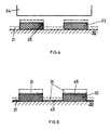
- the lift-off lacquer structure 32 is shown on the substrate 30.
- the plasma 34 of the plasma-assisted deposition process is shown schematically. If the first layer 31 of the color filter layer system, shown in dashed lines in FIG. 4, is to be deposited by a reactive process, in particular using ionized oxygen, then the lift-off lacquer structure, as schematically indicated at 35, is excited in particular in the edge regions Reactive gas, as mentioned in particular O 2 or attacked by in the plasma activated and / or cleaved H 2 O from the residual gas.
- a first way to prevent this is to use the first layer of the color filter layer system non-reactive deposit, So with regard to Fig. 2 and Fig. 3 under ausschliessmaschine Use of the working gas Ar.
- This is the Layer material either directly as a target or evaporation source material used.
- a second and preferred option is to apply to the lift-off lacquer structure, before the first layer 31 of the color filter layer system is applied, an optically broadband and substantially losslessly transmitting, ie optically neutral, well adhering intermediate layer which, as a protective layer , withstand the subsequent process.
- the intermediate layer 45 shown in FIG. 5 with a thickness of 5 to 10 nm preferably consists of SiO or SiO 2 , which is not chemically attacked by excited ionized reactive gas, in particular O 2 or H 2 O from the residual gas.
- the layer 31 indicated by dashed lines denotes the subsequently applied first optically active layer of the color filter layer system, which can now be deposited by a reactive process.
- the intermediate layer 45 may also consist of SiO 2 , which is deposited non-reactive or only weakly reactive. An SiO 2 intermediate layer then forms the first, lower refractive index layer of the filter layer system with the following, higher refractive index layers.
- the intermediate layer is dispensed with.
- the plasma is switched on before the actual coating starts. Therefore, the resist mask comes in contact with O2 / Ar plasma. This rounds the edges of the paint. This makes it difficult the lift-off step or makes a relatively thick Lacquer mask necessary.
- SiO 2 Reactive vapor deposition with APS plasma source
- the procedure according to the invention makes it possible to use pixel structures especially for LCD Lightvalve projectors and CCD sensors, cost-effective and with a low reject rate in addition to environmental changes, in particular temperature and humidity changes, spectrally highly stable.
- Especially under Use of the mentioned intermediate layer is also an extremely achieved good adhesion of the color filter systems on the substrate.
- the necessary lift-off paint layers can be much thinner as twice the color filter layer systems deposited over it be.
- the provision of overhanging side walls of the paint areas, as in the aluminization in semiconductor production usual, is superfluous.
- the preferred use of the mentioned intermediate layer avoids the negative influence on the reactive deposition of the first filter layer on the lift-off lacquer, in particular the edge damage of the lacquer structures by reactive Ar-O 2 -H 2 O plasmas.
Landscapes
- Physics & Mathematics (AREA)
- General Physics & Mathematics (AREA)
- Optics & Photonics (AREA)
- Optical Filters (AREA)
- Liquid Crystal (AREA)
- Physical Vapour Deposition (AREA)
- Solid State Image Pick-Up Elements (AREA)
Abstract
Description
- ergibt mithin wesentlich reduzierte Beschichtungstemperaturen, was zur Reduktion der notwendigen Lackdicke und zur Verwendbarkeit üblicher kostengünstiger Lacke führt. Die sich weiter ergebende Lackdickenreduktion führt direkt zur Reduktion der Ausdehnung der Störbereiche gemäss Fig. 1.
- Durch die Plasmaunterstützung der Beschichtung, sei dies durch Erzeugung geladener Teilchen in einer separaten Plasmakammer, Extraktion durch Gitter in den Beschichtungsraum oder durch Plasmaerzeugung im Beschichtungsraum, wird eine Bombardierung der Substrate mit einem Ionenstrom hoher Dichte realisiert, womit dichte, optisch stabile Filterschichten realisiert werden.
- Die Ausdehnung der durch Abschattung bewirkten Störstellen kann durch zusätzliche Richtmassnahmen, wie Vorsehen von Kolliminatoren oder durch elektrostatische Ausrichtung der Ionenbewegung, reduziert werden. Es werden auch möglichst niedrige Drücke in der Beschichtungskammer eingesetzt, mit entsprechend grosser mittlerer freien Weglänge.
- Fig. 1:
- eine schematische Darstellung eines belackten, strukturierten und beschichteten Substrates zur Erläuterung der Entstehung gestörter Bereiche,
- Fig. 2:
- schematisch eine für die Durchführung des erfindungsgemässen Verfahrens geeignete Sputterbeschichtungsanlage in schematischer Form,
- Fig. 3:
- eine zur Durchführung des erfindungsgemässen Verfahrens geeignete Anlage zum plasmaunterstützten thermischen Aufdampfen, wiederum schematisch dargestellt,
- Fig. 4:
- schematisch eine auf einem Substrat abgelegte Lackstruktur und deren Abrundung der nachfolgenden Beschichtung und
- Fig. 5:
- in Darstellung analog zu Fig. 4 das Vorsehen einer Zwischenschicht zwischen Lackstruktur und nachfolgend abgeschiedener Filterschicht zur Vermeidung der anhand von Fig. 4 erläuterten Verrundung der Kanten des Photolacks.
- EP-508 359 bzw.
US-5 423 970; - EP-564 789 bzw. die US-Anmeldungen
US SN 08/300865
US SN 08/641707.
In Fig. 5 bezeichnet die gestrichelt eingetragene Schicht 31 die nachmals aufgebrachte erste optisch aktive Schicht des Farbfilterschichtsystems, die nun durch einen reaktiven Prozess abgelegt werden kann. Im weiteren kann die Zwischenschicht 45 auch aus SiO2 bestehen, das nicht- oder nur schwach reaktiv abgeschieden wird. Eine SiO2-Zwischenschicht bildet dann die erste, niedrigerbrechende Schicht des Filterschichtsystems mit folgenden, höherbrechenden Schichten.
- Substrat: Glas
- Filterstruktur: Streifen 160 µm breit, 20 mm lang, 100 µm Abstand
- Lackschichtdicke: 3.2 µm
- Lack: Shipley 1045, 6:1 verdünnt.
- opt. Filterschichtsystem: 1,5 µm (d5 von Fig. 1)
- Schichtsystem: SiO2 / TiO2
-
Beschichtungsprozess SiO2: Reaktives Sputtern, Anlage BAS 767
- Quelle: Si-Target
- Sputterleistung: 6.4 kW
- Arbeitsgas: Ar
- Reaktivgas: O2
- Fluss Arbeitsgas: 40 sccm
- Fluss Reaktivgas: 50 sccm
- Rate: 0.3 nm/sec
-
Beschichtungsprozess TiO2: Reaktives Sputtern
- Quelle: Ti-Target
- Sputterleistung: 10 kW
- Arbeitsgas: Ar
- Reaktivgas: O2
- Fluss Arbeitsgas: 40 sccm
- Fluss Reaktivgas: 36 sccm
- Rate: 0.16 nm/sec
- Beschichtungstemperatur: T ≤ 80°C
- neben der Lackmaske (1 von Fig. 1):
- ≤ 10 µm
- Stabilität der Kanten des Filters:
- ≤ 1 nm Kantenshift von 20°C bis 80°C
- Substrat: Glas
- Filterstruktur: Streifen 10 x 10 µm bis 100 x 100 µm
- Lackschichtdicke (d): 0,5 µm - 2 µm
- opt. Filterschicht (d5) : 1,4 µm
- Lack: Shipley 1045, Verdünnung 6:1 bis 1:1
- Schichtsystem: Zwischenschicht SiO, 10 nm dick, SiO2 / TiO2
- Beschichtungsprozess: SiO-Zwischenschicht nichtreaktiv ohne Plasmaunterstützung, SiO2/TiO2 System plasmaunterstütztes Aufdampfen, Anlage LEYBOLD APS 1100
- Quelle E-Strahlverdampfer mit Vierlochtiegel, SiO-Granulat
- Rate: 0.1 nm/sec
- Anlage: BAS 767
- Druck: 1*10-5 mbar
- Quelle: E-Strahlverdampfer mit Vierlochtiegel, SiO2-Granulat
- Rate: 0.6 m/sec
- Entladungsstrom: 50 A
- Biasspannung: 150 V
- UAnode-Kathode: 130 V
- Arbeitsgas: Ar
- Reaktivgas: O2
- Fluss Arbeitsgas: 15 sccm
- Fluss Reaktivgas: 10 sccm
- Totaldruck: 3.5*10-3 mbar
- Quelle: E-Strahlverdampfer mit Vierlochtiegel, TiO-Tabletten
- Rate: 0.3 m/sec
- Entladungsstrom: 50 A
- Biasspannung: 110 - 120 V
- UAnode-Kathode: 100 - 110 V
- Arbeitsgas: Ar
- Reaktivgas: O2
- Fluss Arbeitsgas: 11 sccm
- Fluss Reaktivgas: 35 sccm
- Totaldruck: 4.2*10-3 mbar
- Beschichtungstemperatur: T ≤ 105°C
- Stabilität:
- < 1 nm spektrale Kantenshift von 20°C bis 80°C
- Grösse (1) der gestörten Zone:
- < 2 µm
Claims (6)
- Farbfilterflächenstruktur, abgelegt auf einem Substrat als Feld von Farbfilterschichtsystemen, in unterschiedlichen Spektren wirkend, dadurch gekennzeichnet, dass die dem Substrat zugewandte erste Schicht der Farbfilterschichtsysteme eine in allen unterschiedlichen Spektren optisch im wesentlichen neutrale Schicht ist.
- Farbfilterflächenstruktur nach Anspruch 1, dadurch gekennzeichnet, dass die erste Schicht aus SiO2 besteht.
- Farbfilterflächenstruktur nach Anspruch 1, dadurch gekennzeichnet, dass die erste Schicht aus SiO besteht.
- Farbfilterflächenstruktur, dadurch gekennzeichnet, dass die erste Schicht eine Dicke von 5 - 10 nm hat.
- Farbfilterflächenstruktur nach Anspruch 1, dadurch gekennzeichnet, dass die erste Schicht eine niedriger brechende Schicht der Farbfilterschichtsysteme ist, welcher höher brechende Schichten folgen.
- Verwendung der Farbfilterflächenstruktur nach einem der Ansprüche 1 bis 5 an LCD-Lightalve-Projektoren oder für die Farbgebung für CCD-Sensoren.
Applications Claiming Priority (5)
| Application Number | Priority Date | Filing Date | Title |
|---|---|---|---|
| CH4171998 | 1998-02-20 | ||
| CH7199841 | 1998-02-20 | ||
| CH00417/98A CH693076A5 (de) | 1998-02-20 | 1998-02-20 | Verfahren zur Herstellung einer Farbfilterschichtsystem-Struktur auf einer Unterlage. |
| EP99900426A EP1057052B2 (de) | 1998-02-20 | 1999-01-21 | Verfahren zur herstellung einer struktur von interferenz-farbfiltern |
| PCT/CH1999/000026 WO1999042864A1 (de) | 1998-02-20 | 1999-01-21 | Verfahren zur herstellung einer struktur von interferenz-farbfiltern |
Related Parent Applications (1)
| Application Number | Title | Priority Date | Filing Date |
|---|---|---|---|
| EP99900426A Division EP1057052B2 (de) | 1998-02-20 | 1999-01-21 | Verfahren zur herstellung einer struktur von interferenz-farbfiltern |
Publications (3)
| Publication Number | Publication Date |
|---|---|
| EP1437606A2 true EP1437606A2 (de) | 2004-07-14 |
| EP1437606A3 EP1437606A3 (de) | 2004-12-08 |
| EP1437606B1 EP1437606B1 (de) | 2018-07-18 |
Family
ID=4186565
Family Applications (2)
| Application Number | Title | Priority Date | Filing Date |
|---|---|---|---|
| EP99900426A Expired - Lifetime EP1057052B2 (de) | 1998-02-20 | 1999-01-21 | Verfahren zur herstellung einer struktur von interferenz-farbfiltern |
| EP04000793.2A Expired - Lifetime EP1437606B1 (de) | 1998-02-20 | 1999-01-21 | Verfahren zur Herstellung einer Struktur von Interferenz-Farbfiltern |
Family Applications Before (1)
| Application Number | Title | Priority Date | Filing Date |
|---|---|---|---|
| EP99900426A Expired - Lifetime EP1057052B2 (de) | 1998-02-20 | 1999-01-21 | Verfahren zur herstellung einer struktur von interferenz-farbfiltern |
Country Status (8)
| Country | Link |
|---|---|
| US (3) | US6468703B1 (de) |
| EP (2) | EP1057052B2 (de) |
| JP (3) | JP2002504699A (de) |
| CH (1) | CH693076A5 (de) |
| DE (1) | DE59908652D1 (de) |
| ES (1) | ES2214837T3 (de) |
| TW (1) | TW420823B (de) |
| WO (1) | WO1999042864A1 (de) |
Families Citing this family (10)
| Publication number | Priority date | Publication date | Assignee | Title |
|---|---|---|---|---|
| CH693076A5 (de) * | 1998-02-20 | 2003-02-14 | Unaxis Trading Ag | Verfahren zur Herstellung einer Farbfilterschichtsystem-Struktur auf einer Unterlage. |
| DE102004034418B4 (de) * | 2004-07-15 | 2009-06-25 | Schott Ag | Verfahren zur Herstellung struktuierter optischer Filterschichten auf Substraten |
| DE102004034419B4 (de) * | 2004-07-15 | 2009-05-07 | Schott Ag | Verfahren und Vorrichtung zur Herstellung mehrlagiger, strukturierter Farbfilter |
| DE102009034532A1 (de) * | 2009-07-23 | 2011-02-03 | Msg Lithoglas Ag | Verfahren zum Herstellen einer strukturierten Beschichtung auf einem Substrat, beschichtetes Substrat sowie Halbzeug mit einem beschichteten Substrat |
| US20140233126A1 (en) * | 2011-05-31 | 2014-08-21 | Suzhou University | Reflective color filter |
| CN102590917B (zh) * | 2012-03-12 | 2014-05-14 | 杭州麦乐克电子科技有限公司 | 3.65微米至5微米宽带红外滤光片 |
| US10197716B2 (en) | 2012-12-19 | 2019-02-05 | Viavi Solutions Inc. | Metal-dielectric optical filter, sensor device, and fabrication method |
| KR102465995B1 (ko) * | 2015-09-30 | 2022-11-25 | 삼성전자주식회사 | 색분할기 구조와 그 제조방법, 색분할기 구조를 포함하는 이미지센서 및 이미지센서를 포함하는 광학장치 |
| US11156753B2 (en) | 2017-12-18 | 2021-10-26 | Viavi Solutions Inc. | Optical filters |
| JP6847996B2 (ja) * | 2019-04-02 | 2021-03-24 | ヴァイアヴィ・ソリューションズ・インコーポレイテッドViavi Solutions Inc. | 金属誘電体光学フィルター、センサーデバイス、および製造方法 |
Family Cites Families (26)
| Publication number | Priority date | Publication date | Assignee | Title |
|---|---|---|---|---|
| US3914464A (en) * | 1971-04-19 | 1975-10-21 | Optical Coating Laboratory Inc | Striped dichroic filter and method for making the same |
| US3771857A (en) † | 1971-04-19 | 1973-11-13 | Optical Coating Laboratory Inc | Striped dichroic filter and method for making the same |
| JPS50147339A (de) * | 1974-05-16 | 1975-11-26 | ||
| US3996461A (en) * | 1975-03-31 | 1976-12-07 | Texas Instruments Incorporated | Silicon photosensor with optical thin film filter |
| US4155627A (en) * | 1976-02-02 | 1979-05-22 | Rca Corporation | Color diffractive subtractive filter master recording comprising a plurality of superposed two-level relief patterns on the surface of a substrate |
| JPS53135348A (en) * | 1977-04-30 | 1978-11-25 | Toshiba Corp | Etching method for multilayer film |
| US4433470A (en) * | 1981-05-19 | 1984-02-28 | Tokyo Shibaura Denki Kabushiki Kaisha | Method for manufacturing semiconductor device utilizing selective etching and diffusion |
| US5144498A (en) * | 1990-02-14 | 1992-09-01 | Hewlett-Packard Company | Variable wavelength light filter and sensor system |
| US5164858A (en) * | 1990-03-07 | 1992-11-17 | Deposition Sciences, Inc. | Multi-spectral filter |
| US5246803A (en) * | 1990-07-23 | 1993-09-21 | Eastman Kodak Company | Patterned dichroic filters for solid state electronic image sensors |
| ATE144004T1 (de) * | 1991-04-12 | 1996-10-15 | Balzers Hochvakuum | Verfahren und anlage zur beschichtung mindestens eines gegenstandes |
| JP2526182B2 (ja) * | 1991-05-24 | 1996-08-21 | 株式会社日本製鋼所 | 化合物薄膜の形成方法及び装置 |
| JP3036136B2 (ja) * | 1991-08-16 | 2000-04-24 | 凸版印刷株式会社 | パターン状多層干渉膜の形成方法 |
| JPH0667018A (ja) * | 1992-08-19 | 1994-03-11 | Tokai Rubber Ind Ltd | 薄膜光フィルターの製法 |
| DE4407067C2 (de) * | 1994-03-03 | 2003-06-18 | Unaxis Balzers Ag | Dielektrisches Interferenz-Filtersystem, LCD-Anzeige und CCD-Anordnung sowie Verfahren zur Herstellung eines dielektrischen Interferenz-Filtersystems |
| JP3232866B2 (ja) * | 1994-04-06 | 2001-11-26 | 株式会社日立製作所 | カラー液晶表示装置の製造方法 |
| US5502595A (en) * | 1994-06-03 | 1996-03-26 | Industrial Technology Research Institute | Color filters and their preparation |
| JPH0894831A (ja) * | 1994-09-26 | 1996-04-12 | Olympus Optical Co Ltd | カラーフィルター |
| US5510215A (en) * | 1995-01-25 | 1996-04-23 | Eastman Kodak Company | Method for patterning multilayer dielectric color filter |
| JPH09219505A (ja) * | 1996-02-08 | 1997-08-19 | Olympus Optical Co Ltd | カラー固体撮像装置 |
| JPH09318808A (ja) * | 1996-05-29 | 1997-12-12 | Toppan Printing Co Ltd | カラーフィルターの製造方法 |
| US6154265A (en) * | 1996-06-18 | 2000-11-28 | Canon Kabushiki Kaisha | Liquid crystal device and production process thereof |
| US5726805A (en) * | 1996-06-25 | 1998-03-10 | Sandia Corporation | Optical filter including a sub-wavelength periodic structure and method of making |
| US5915051A (en) * | 1997-01-21 | 1999-06-22 | Massascusetts Institute Of Technology | Wavelength-selective optical add/drop switch |
| JP3829412B2 (ja) * | 1997-05-28 | 2006-10-04 | Jsr株式会社 | カラーフィルタ用感放射線性組成物 |
| CH693076A5 (de) * | 1998-02-20 | 2003-02-14 | Unaxis Trading Ag | Verfahren zur Herstellung einer Farbfilterschichtsystem-Struktur auf einer Unterlage. |
-
1998
- 1998-02-20 CH CH00417/98A patent/CH693076A5/de not_active IP Right Cessation
-
1999
- 1999-01-21 JP JP2000532744A patent/JP2002504699A/ja active Pending
- 1999-01-21 ES ES99900426T patent/ES2214837T3/es not_active Expired - Lifetime
- 1999-01-21 EP EP99900426A patent/EP1057052B2/de not_active Expired - Lifetime
- 1999-01-21 WO PCT/CH1999/000026 patent/WO1999042864A1/de not_active Ceased
- 1999-01-21 EP EP04000793.2A patent/EP1437606B1/de not_active Expired - Lifetime
- 1999-01-21 DE DE59908652T patent/DE59908652D1/de not_active Expired - Lifetime
- 1999-02-19 TW TW088102404A patent/TW420823B/zh not_active IP Right Cessation
-
2000
- 2000-08-18 US US09/641,486 patent/US6468703B1/en not_active Expired - Lifetime
-
2002
- 2002-07-25 US US10/205,088 patent/US6879450B2/en not_active Expired - Lifetime
-
2005
- 2005-03-10 US US11/076,691 patent/US7632629B2/en not_active Expired - Fee Related
-
2009
- 2009-10-14 JP JP2009237488A patent/JP4871987B2/ja not_active Expired - Lifetime
-
2010
- 2010-05-21 JP JP2010117421A patent/JP5113879B2/ja not_active Expired - Lifetime
Also Published As
| Publication number | Publication date |
|---|---|
| JP4871987B2 (ja) | 2012-02-08 |
| US7632629B2 (en) | 2009-12-15 |
| JP2010009078A (ja) | 2010-01-14 |
| DE59908652D1 (de) | 2004-04-01 |
| JP5113879B2 (ja) | 2013-01-09 |
| EP1057052B8 (de) | 2004-03-10 |
| JP2002504699A (ja) | 2002-02-12 |
| US20050157414A1 (en) | 2005-07-21 |
| EP1437606A3 (de) | 2004-12-08 |
| EP1057052B2 (de) | 2010-07-21 |
| TW420823B (en) | 2001-02-01 |
| ES2214837T3 (es) | 2004-09-16 |
| EP1057052A1 (de) | 2000-12-06 |
| US6879450B2 (en) | 2005-04-12 |
| EP1057052B1 (de) | 2004-01-21 |
| EP1437606B1 (de) | 2018-07-18 |
| CH693076A5 (de) | 2003-02-14 |
| JP2010250329A (ja) | 2010-11-04 |
| US6468703B1 (en) | 2002-10-22 |
| WO1999042864A1 (de) | 1999-08-26 |
| HK1034118A1 (en) | 2001-10-12 |
| US20020196568A1 (en) | 2002-12-26 |
Similar Documents
| Publication | Publication Date | Title |
|---|---|---|
| EP0529268B1 (de) | Harte Entspiegelungsschicht für Kunststofflinsen | |
| EP1437606B1 (de) | Verfahren zur Herstellung einer Struktur von Interferenz-Farbfiltern | |
| EP2735018B1 (de) | Verfahren und vorrichtung zur herstellung partikelarmer schichten auf substraten | |
| DE202004019052U1 (de) | Aufbau diffraktiver Optiken durch strukturierte Glasbeschichtung | |
| DE10228946A1 (de) | Optischer Modulator | |
| DE4324325B4 (de) | Verfahren zur Herstellung eines Bauelementes, optisches Bauelement, Verwendung desselben und Vakuumbehandlungsanlage zu seiner Herstellung | |
| DE102009034532A1 (de) | Verfahren zum Herstellen einer strukturierten Beschichtung auf einem Substrat, beschichtetes Substrat sowie Halbzeug mit einem beschichteten Substrat | |
| EP1778889A1 (de) | Reinraumfähige beschichtungsanlage | |
| EP0838535B1 (de) | Interferenzschichtensystem | |
| JP7310360B2 (ja) | 薄膜の製造方法 | |
| US6692850B2 (en) | Controlled stress optical coatings for membranes | |
| EP3133184B1 (de) | Verfahren zum ausbilden einer schicht mit hoher lichttransmission und/oder niedriger lichtreflexion | |
| DE3442208A1 (de) | Verfahren und vorrichtung zum herstellen harten kohlenstoffschichten | |
| DE102012100288B4 (de) | Verfahren zur Herstellung eines Kunststoffsubstrats mit einer porösen Schicht | |
| EP3417086B1 (de) | Vorrichtung und verfahren zur herstellung definierter eigenschaften von gradientenschichten in einem system mehrlagiger beschichtungen bei sputter-anlagen | |
| EP1655385B1 (de) | Verfahren zum Aufbringen optischer Beschichtungen | |
| EP0961806B1 (de) | Verfahren zur modifizierung von substratoberflächen aus polymeren oder copolymeren mit methacrylatanteil | |
| HK1071787A (en) | Method of making a structure of interference filters | |
| HK1034118B (en) | Method for producing a structure of interference colour filters | |
| WO2025176417A1 (de) | Verfahren zur herstellung zonaler beschichtungen auf optischen oberflächen | |
| EP2420587B1 (de) | Verfahren zur Erzeugung einer farbigen Überzugsschicht mittels Kathodenstrahlzerstäuben | |
| DD241175A1 (de) | Verfahren zur herstellung transparenter leiterbahnen fuer elektrolumineszenzdisplays | |
| DE102006027098A1 (de) | Verfahren und Vorrichtung zur Schichtoptimierung mittels Radikale |
Legal Events
| Date | Code | Title | Description |
|---|---|---|---|
| PUAI | Public reference made under article 153(3) epc to a published international application that has entered the european phase |
Free format text: ORIGINAL CODE: 0009012 |
|
| AC | Divisional application: reference to earlier application |
Ref document number: 1057052 Country of ref document: EP Kind code of ref document: P |
|
| AK | Designated contracting states |
Kind code of ref document: A2 Designated state(s): BE DE ES FI FR GB IT NL SE |
|
| PUAL | Search report despatched |
Free format text: ORIGINAL CODE: 0009013 |
|
| AK | Designated contracting states |
Kind code of ref document: A3 Designated state(s): BE DE ES FI FR GB IT NL SE |
|
| RIC1 | Information provided on ipc code assigned before grant |
Ipc: 7G 02B 5/28 B Ipc: 7H 01J 9/233 B Ipc: 7G 02B 1/10 A Ipc: 7G 02B 5/20 B |
|
| 17P | Request for examination filed |
Effective date: 20050426 |
|
| REG | Reference to a national code |
Ref country code: HK Ref legal event code: DE Ref document number: 1071787 Country of ref document: HK |
|
| AKX | Designation fees paid |
Designated state(s): BE DE ES FI FR GB IT NL SE |
|
| 17Q | First examination report despatched |
Effective date: 20121022 |
|
| RAP1 | Party data changed (applicant data changed or rights of an application transferred) |
Owner name: OERLIKON TRADING AG, TRUEBBACH |
|
| GRAP | Despatch of communication of intention to grant a patent |
Free format text: ORIGINAL CODE: EPIDOSNIGR1 |
|
| INTG | Intention to grant announced |
Effective date: 20171205 |
|
| GRAS | Grant fee paid |
Free format text: ORIGINAL CODE: EPIDOSNIGR3 |
|
| GRAJ | Information related to disapproval of communication of intention to grant by the applicant or resumption of examination proceedings by the epo deleted |
Free format text: ORIGINAL CODE: EPIDOSDIGR1 |
|
| GRAL | Information related to payment of fee for publishing/printing deleted |
Free format text: ORIGINAL CODE: EPIDOSDIGR3 |
|
| INTC | Intention to grant announced (deleted) | ||
| RAP1 | Party data changed (applicant data changed or rights of an application transferred) |
Owner name: OERLIKON SURFACE SOLUTIONS AG, PFAEFFIKON |
|
| GRAR | Information related to intention to grant a patent recorded |
Free format text: ORIGINAL CODE: EPIDOSNIGR71 |
|
| GRAA | (expected) grant |
Free format text: ORIGINAL CODE: 0009210 |
|
| AC | Divisional application: reference to earlier application |
Ref document number: 1057052 Country of ref document: EP Kind code of ref document: P |
|
| AK | Designated contracting states |
Kind code of ref document: B1 Designated state(s): BE DE ES FI FR GB IT NL SE |
|
| INTG | Intention to grant announced |
Effective date: 20180611 |
|
| REG | Reference to a national code |
Ref country code: GB Ref legal event code: FG4D Free format text: NOT ENGLISH |
|
| REG | Reference to a national code |
Ref country code: DE Ref legal event code: R096 Ref document number: 59915477 Country of ref document: DE |
|
| REG | Reference to a national code |
Ref country code: NL Ref legal event code: MP Effective date: 20180718 |
|
| PG25 | Lapsed in a contracting state [announced via postgrant information from national office to epo] |
Ref country code: NL Free format text: LAPSE BECAUSE OF FAILURE TO SUBMIT A TRANSLATION OF THE DESCRIPTION OR TO PAY THE FEE WITHIN THE PRESCRIBED TIME-LIMIT Effective date: 20180718 |
|
| REG | Reference to a national code |
Ref country code: DE Ref legal event code: R071 Ref document number: 59915477 Country of ref document: DE |
|
| PG25 | Lapsed in a contracting state [announced via postgrant information from national office to epo] |
Ref country code: SE Free format text: LAPSE BECAUSE OF FAILURE TO SUBMIT A TRANSLATION OF THE DESCRIPTION OR TO PAY THE FEE WITHIN THE PRESCRIBED TIME-LIMIT Effective date: 20180718 Ref country code: FI Free format text: LAPSE BECAUSE OF FAILURE TO SUBMIT A TRANSLATION OF THE DESCRIPTION OR TO PAY THE FEE WITHIN THE PRESCRIBED TIME-LIMIT Effective date: 20180718 |
|
| RIC2 | Information provided on ipc code assigned after grant |
Ipc: G02B 1/10 20150101AFI20040518BHEP Ipc: G02B 5/28 20060101ALI20041020BHEP Ipc: H01J 9/233 20060101ALI20041020BHEP Ipc: G02B 5/20 20060101ALI20041020BHEP |
|
| REG | Reference to a national code |
Ref country code: BE Ref legal event code: MK Effective date: 20190121 |
|
| PG25 | Lapsed in a contracting state [announced via postgrant information from national office to epo] |
Ref country code: ES Free format text: LAPSE BECAUSE OF FAILURE TO SUBMIT A TRANSLATION OF THE DESCRIPTION OR TO PAY THE FEE WITHIN THE PRESCRIBED TIME-LIMIT Effective date: 20180718 |
|
| REG | Reference to a national code |
Ref country code: DE Ref legal event code: R097 Ref document number: 59915477 Country of ref document: DE |
|
| REG | Reference to a national code |
Ref country code: GB Ref legal event code: PE20 Expiry date: 20190120 |
|
| PLBE | No opposition filed within time limit |
Free format text: ORIGINAL CODE: 0009261 |
|
| STAA | Information on the status of an ep patent application or granted ep patent |
Free format text: STATUS: NO OPPOSITION FILED WITHIN TIME LIMIT |
|
| 26N | No opposition filed |
Effective date: 20190423 |
|
| PG25 | Lapsed in a contracting state [announced via postgrant information from national office to epo] |
Ref country code: GB Free format text: LAPSE BECAUSE OF EXPIRATION OF PROTECTION Effective date: 20190120 |