EP1437610A1 - Unité pour rétroéclairage - Google Patents
Unité pour rétroéclairage Download PDFInfo
- Publication number
- EP1437610A1 EP1437610A1 EP20030011835 EP03011835A EP1437610A1 EP 1437610 A1 EP1437610 A1 EP 1437610A1 EP 20030011835 EP20030011835 EP 20030011835 EP 03011835 A EP03011835 A EP 03011835A EP 1437610 A1 EP1437610 A1 EP 1437610A1
- Authority
- EP
- European Patent Office
- Prior art keywords
- light
- holographic pattern
- backlight unit
- guide panel
- light guide
- Prior art date
- Legal status (The legal status is an assumption and is not a legal conclusion. Google has not performed a legal analysis and makes no representation as to the accuracy of the status listed.)
- Granted
Links
Images




Classifications
-
- G—PHYSICS
- G02—OPTICS
- G02B—OPTICAL ELEMENTS, SYSTEMS OR APPARATUS
- G02B6/00—Light guides; Structural details of arrangements comprising light guides and other optical elements, e.g. couplings
- G02B6/0001—Light guides; Structural details of arrangements comprising light guides and other optical elements, e.g. couplings specially adapted for lighting devices or systems
- G02B6/0011—Light guides; Structural details of arrangements comprising light guides and other optical elements, e.g. couplings specially adapted for lighting devices or systems the light guides being planar or of plate-like form
- G02B6/0033—Means for improving the coupling-out of light from the light guide
- G02B6/0035—Means for improving the coupling-out of light from the light guide provided on the surface of the light guide or in the bulk of it
- G02B6/0038—Linear indentations or grooves, e.g. arc-shaped grooves or meandering grooves, extending over the full length or width of the light guide
-
- G—PHYSICS
- G02—OPTICS
- G02F—OPTICAL DEVICES OR ARRANGEMENTS FOR THE CONTROL OF LIGHT BY MODIFICATION OF THE OPTICAL PROPERTIES OF THE MEDIA OF THE ELEMENTS INVOLVED THEREIN; NON-LINEAR OPTICS; FREQUENCY-CHANGING OF LIGHT; OPTICAL LOGIC ELEMENTS; OPTICAL ANALOGUE/DIGITAL CONVERTERS
- G02F1/00—Devices or arrangements for the control of the intensity, colour, phase, polarisation or direction of light arriving from an independent light source, e.g. switching, gating or modulating; Non-linear optics
- G02F1/01—Devices or arrangements for the control of the intensity, colour, phase, polarisation or direction of light arriving from an independent light source, e.g. switching, gating or modulating; Non-linear optics for the control of the intensity, phase, polarisation or colour
- G02F1/13—Devices or arrangements for the control of the intensity, colour, phase, polarisation or direction of light arriving from an independent light source, e.g. switching, gating or modulating; Non-linear optics for the control of the intensity, phase, polarisation or colour based on liquid crystals, e.g. single liquid crystal display cells
- G02F1/133—Constructional arrangements; Operation of liquid crystal cells; Circuit arrangements
- G02F1/1333—Constructional arrangements; Manufacturing methods
- G02F1/1335—Structural association of cells with optical devices, e.g. polarisers or reflectors
-
- G—PHYSICS
- G02—OPTICS
- G02B—OPTICAL ELEMENTS, SYSTEMS OR APPARATUS
- G02B6/00—Light guides; Structural details of arrangements comprising light guides and other optical elements, e.g. couplings
- G02B6/0001—Light guides; Structural details of arrangements comprising light guides and other optical elements, e.g. couplings specially adapted for lighting devices or systems
- G02B6/0011—Light guides; Structural details of arrangements comprising light guides and other optical elements, e.g. couplings specially adapted for lighting devices or systems the light guides being planar or of plate-like form
- G02B6/0066—Light guides; Structural details of arrangements comprising light guides and other optical elements, e.g. couplings specially adapted for lighting devices or systems the light guides being planar or of plate-like form characterised by the light source being coupled to the light guide
- G02B6/0068—Arrangements of plural sources, e.g. multi-colour light sources
Definitions
- the present invention relates to a backlight unit, and more particularly, to an edge light type backlight unit using a light guide panel (LGP).
- LGP light guide panel
- a light receiving type flat panel display device such as a liquid crystal display device forms an image not by emitting light by itself but by receiving light from the outside, the image cannot be viewed in a dark place.
- a backlight unit for emitting light is installed at a rear surface of the light receiving type flat panel display device.
- the backlight unit can be classified into a direct light type and an edge light type according to the arrangement type of a light source.
- the edge light type light source can use a linear light source and a point light source as a light source.
- a typical linear light source there is a cold cathode fluorescent lamp (CCFL) in which electrodes are installed inside a tube at both end portions.
- a light emitting diode (LED) is a typical linear light source.
- the CCFL can emit a strong white light and obtain a high brightness and a high uniformity.
- the CCFL can enable a large size design of a device.
- the CCFL is disadvantageous since it is operated by a high frequency AC signal and has a narrow operational temperature range.
- the LED exhibits a lower performance in the brightness and uniformity compared to the CCFL, but is operated by a DC signal and has a long life span and a wide operational temperature range. Further, the LED can be manufactured thin.
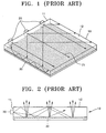
- FIG. 1 is a perspective view illustrating a conventional edge light type backlight unit using a point light source.
- FIG. 2 is a sectional view illustrating the edge light type backlight unit shown in FIG. 1.
- three LEDs 20 are installed at an edge 11 of a light guide panel 10 as point light sources.
- a holographic pattern 30 for making the light emitted from the LEDs 20 proceed through a light exhaust surface 12 is formed on a lower surface of the light guide panel 10.
- the light emitted from each of the LEDs 20 is incident on the light guide panel 10 through the edge 11 and then input to the holographic pattern 30.
- the holographic pattern 30 having a diffraction grid structure formed perpendicular to an optical axis 21 changes the incident light to a surface light and makes the surface light proceed through the light exhaust surface 12 which is an upper surface of the light guide panel 10.
- the holographic pattern 30 can emit light at the highest efficiency when the light is incident on the holographic pattern 30 at an angle of 90°. Also, as the distribution of an incident azimuth angle of the light incident on the holographic pattern 30 decreases, a uniform brightness can be obtained at the light exhaust surface 12.
- a screen appears to be smeared. In a narrow range of about 1 centimeter, a change in brightness of about 0.9 is detected as a smear. However, when the brightness changes gradually from the central portion of the screen to an edge portion thereof, a change in brightness of about 0.8 is not detected as a smear. Thus, a uniformity of brightness over 0.8 is needed. In particular, to obtain a quality image, a uniformity of brightness over 0.9 is needed.
- FIG. 4 shows the distribution of the output of light by the conventional backlight unit shown in FIG. 1.
- the light guide panel 10 is divided into three portions, that is, a near portion 40, a middle portion 50, and a far portion 60, sequentially from the edge 11 where the LEDs 20 are installed, where the distribution of the output of light is shown.
- the middle portion 50 and the far portion 60 have a wider light output distribution compared to the near portion 40.
- FIG. 5 is a graph showing the brightness at the light exhaust surface 12 by the edge light type backlight unit shown in FIG. 1.
- the vertical axis indicates brightness and the horizontal axis indicates FWHM (full width half maximum) showing a light exhaust angle at the light exhaust surface 12.
- Three curves C1, C2, and C3 from the left side indicate the brightness of the near portion 40, the middle portion 50, and the far portion 60, respectively. Referring to FIG. 5, it can be seen that the brightness of the near portion 40 is greater than those of the middle portion 50 and the far portion 60.
- the FWHM of the near portion 40 is 20°/20° while those of the middle portion 50 and the far portion 60 are 20°/35° which are relatively wider than that of the near portion 40.
- the first angle "20°”and the second angle "35°” denote FWHMs in an X direction and a Y direction, respectively.
- the irregularity of brightness is because the distribution of an incident azimuth angle of the light incident on the holographic pattern 30 is different in each of the near portion 40, the middle portion 50, and the far portion 60 so that an efficiency in the light emission by the holographic pattern 30 and the distribution of an exhaust azimuth angle of the exhaust light are different in the three portions.
- the present invention provides a backlight unit which can reduce the incident azimuth angle range of light incident on a holographic pattern in a light guide panel.
- a backlight unit comprises a point light source emitting light and a light guide panel including a holographic pattern formed of shapes having a common center at the point light source.
- the shapes forming the holographic pattern can be concentric circles.
- the shapes forming the holographic pattern can be concentric polygons.
- the holographic pattern is formed on at least one of a bottom surface of the light guide panel and an upper surface facing the bottom surface.
- the point light source can be installed at a corner of the light guide panel .
- the point light source can be installed close to an edge of the light guide panel.
- an LED 120 is installed at a corner of a light guide panel 110 as a point light source.
- the light guide panel 110 is manufactured of a transparent material transmitting light. Typically, acryl based transparent resin (PMMA) exhibiting a refractive index of about 1.49 and a specific gravity of about 1.19, or olefin based transparent resin exhibiting a special gravity of about 1.0 for lightness, is used for the light guide panel 110.
- PMMA acryl based transparent resin
- the light guide panel 110 is usually 2-3 mm thick and may have a wedge shape so that the thickness of the light guide panel 110 decreases from an edge on which light is incident to the opposite edge to reduce the weight thereof.
- the size of the light guide panel 110 is dependent on the size of an image display device (not shown), for example, an LCD (liquid crystal display), which is installed at a light exhaust surface 112.
- the LED 120 which is an exampled of a point light source emits light in a range between ⁇ 90° with respect to an optical axis as shown in FIG. 3.
- An angle at which light having an intensity corresponding to the half (Imax/2) of the maximum value (Imax) of the intensity of light is referred as an FWHM.
- the FWHM is about ⁇ 45.
- a 1-chip-2-LED type or a 2-chip-1-LED type can be used for the LED 120.
- An appropriate LED can be used according to a required brightness.
- the LED 120 is installed at a corner of the light guide panel 110.
- the corner of the light guide panel 110 is chamfered, as shown in FIG. 6.
- the LED 120 is preferably installed so as to emit light to a light incident surface 111 formed by chamfering.
- a holographic pattern 130 is formed at the light guide panel 110.
- the holographic pattern 130 is a diffraction grating which diffracts the light emitted from the LED 120 and incident on the light guide panel 110 so as to be exhausted through the light exhaust surface 112.
- the holographic pattern 130 is formed on a bottom surface of the light guide panel 110 forming concentric circles having the common center at the LED 120.
- a reflection panel for reflecting the light diffracted by the holographic pattern 130 upward is provided at a lower surface of the holographic pattern 130.
- the diffraction grating preferably has a period of 2 ⁇ m or less and may have a period of about 0.4 ⁇ m and a depth of about 0.2 ⁇ m, for example.
- the period means an interval between the concentric circles.
- the period and depth are not limited to the above values and can be appropriately adjusted to make the distribution of the output of light at the light exhaust surface 112 uniform.
- the holographic pattern 130 can be formed on an upper surface facing
- FIG. 7 is a plan view illustrating a backlight unit according to another preferred embodiment of the present invention.
- the LED 120 is installed at a left edge 113 of the light guide panel 110.
- the LED 120 can be installed at the other edges of the light guide panel 110.
- the holographic pattern 130 is the above-described diffraction grating and formed on the bottom surface and/or the upper surface of the light guide panel 110, forming concentric circles having the center at the LED 120.
- a diffusion member 150 for diffusing the light emitted from the LED 120 can be further provided between the LED 120 and the light guide panel 110.
- a concave lens, for example, may be used as the diffusion member 150.
- the diffusion member 150 diffuses the light emitted from the LED 120 so that the light is incident on the entire area of the left edge 113 of the light guide panel 110 at its maximum.
- the light emitted from the LED 120 is incident on the light guide panel 110 through the light incident surface 111 and proceeds in a radial direction.
- the light is diffracted by the holographic pattern 130 in the light guide panel 110 and reflected by the reflection panel (not shown) to be exhausted through the light exhaust surface 112.
- the diffusion panel (not shown) for diffusing the light output from the light exhaust surface 112 to be emitted with a uniform intensity is further provided above the light guide panel 110.
- the light passing through the diffusion panel is incident on a flat display device such as a LCD device (not shown), which is disposed above the diffusion panel.
- the holographic pattern 130 emits light at the highest efficiency when the light is incident at an angle of 90° with respect to the holographic pattern 130.
- the holographic pattern 130 is formed as concentric circles having the center at the LED 120.
- An incident azimuth angle A of light incident on the holographic pattern 130 is almost 90° at an arbitrary point in the light guide panel 110 and is almost uniform.
- the holographic pattern 130 can emit light to the light exhaust surface 112 by diffracting the light at the maximum efficiency.
- the azimuth angle of the light exhausted to the light exhaust surface 112 is 80° or more with respect to the light exhaust surface 112, preferably, almost 90°, which is almost uniform, the intensity of the exhaust light can be easily adjusted and the brightness at the light exhaust surface 112 is made uniform.
- the conventional backlight unit shown in FIG. 1 includes a diffusion panel (not shown) for diffusing light emitted from the light exhaust surface 12 and a prism panel (not shown) for improving brightness of the diffused light in a normal direction thereof, that is, in a direction perpendicular to the light exhaust surface 112.
- a prism panel (not shown) for improving brightness of the diffused light in a normal direction thereof, that is, in a direction perpendicular to the light exhaust surface 112.
- two prism panels are typically used and the prism panels are arranged such that the prism patterns of the prism panels cross each other perpendicularly.
- the prism panel is not needed.
- the number of media through which the light passes can be reduced.
- the amount of light absorbed by each medium is reduced so that an efficiency of use of light can be improved.
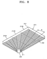
- FIG. 8 is a perspective view illustrating a backlight unit according to yet another preferred embodiment of the present invention.
- an LED 220 is installed at a corner of a light guide panel 210 as a point light source.
- a holographic pattern 230 is formed on a bottom surface of the light guide panel 210 or an upper surface thereof facing the bottom surface.
- a reflection panel for reflecting light can be further provided under the holographic pattern 230.
- the light guide panel 210 can be manufactured of a transparent material such as acryl based transparent resin PMMA or olefin based transparent resin which transmits light, like the light guide panel 110 as shown in FIG. 6.
- the comer is chamfered as shown in FIG. 8 and the LED 220 is preferably installed to emit light to an incident light surface 211 formed by chamfering.
- the holographic pattern 230 is diffracts the light emitted from the LED 220 and incident on the light guide panel 210 so as to be exhausted through the light exhaust surface 212.
- the holographic pattern 230 has a shape of polygons inscribed inside concentric circles having the common center at the LED 220.
- the holographic pattern 230 can be formed to have a shape of equilateral polygons in which the central angles of all sides are identical. Also, The holographic pattern 230 can be formed to have a shape of polygons in which each side has a different central angle.
- the holographic pattern 230 has a shape of equilateral polygons in which the central angel B of each side is 10°.
- the distribution of an incident azimuth angle of the light incident on the holographic pattern 230 in the entire area in the light guide panel 210 is within 90 ⁇ 5° with respect to the holographic pattern 230.
- the central angle B decreases, the distribution of an incident azimuth angle of the light incident on the holographic pattern 230 decreases so that the distribution is close to a concentric circle having the center at the LED 120 as shown in FIG. 6.
- Whether to make the shape of the holographic pattern 230 equilateral polygon s and how to set the central angle can be appropriately determined considering the uniformity of brightness required by the light exhaust surface 212 and an efficiency of use of light.
- the LED 220 can be installed at an edge of the light guide panel 210, and a diffusion member 250 such as a concave lens for diffusing light can be further provided between the LED 220 and the light guide panel 210.
- FIGS. 10 through 12 are graphs showing the results of measurements of the distribution of brightness at a light exhaust surface in each of three areas 210A, 210B, and 210C of the light guide panel in the preferred embodiment shown in FIG. 8.
- the distributions of brightness shown in FIGS. 10 through 12 are those of light prior to the diffusion panel (not shown). Referring to FIGS. 10 through 12, it can be seen that the distribution of brightness is concentrated at the central portion of each graph and there is little difference in the distribution of brightness according to the portion. This means that an incident azimuth angle of light incident on the holographic pattern 230 is almost concentrated on around 90°. Thus, when a diffusion panel is installed at the light exhaust surface 212, almost uniform distribution of brightness can be obtained from the entire area of the light exhaust surface 212.
- the incident azimuth angle of light incident on the holographic pattern can be made constant, an efficiency of light exhausted through the light exhaust surface can be improved. Also, since the distribution of the exhaust azimuth angle of the exhaust light can be made uniform, a uniform brightness can be obtained from the exhaust surface.
Landscapes
- Physics & Mathematics (AREA)
- General Physics & Mathematics (AREA)
- Optics & Photonics (AREA)
- Nonlinear Science (AREA)
- Mathematical Physics (AREA)
- Chemical & Material Sciences (AREA)
- Crystallography & Structural Chemistry (AREA)
- Planar Illumination Modules (AREA)
- Light Guides In General And Applications Therefor (AREA)
- Liquid Crystal (AREA)
- Diffracting Gratings Or Hologram Optical Elements (AREA)
Applications Claiming Priority (2)
| Application Number | Priority Date | Filing Date | Title |
|---|---|---|---|
| KR2003000781 | 2003-01-07 | ||
| KR1020030000781A KR100624408B1 (ko) | 2003-01-07 | 2003-01-07 | 백라이트 유닛 |
Publications (2)
| Publication Number | Publication Date |
|---|---|
| EP1437610A1 true EP1437610A1 (fr) | 2004-07-14 |
| EP1437610B1 EP1437610B1 (fr) | 2012-08-01 |
Family
ID=32501486
Family Applications (1)
| Application Number | Title | Priority Date | Filing Date |
|---|---|---|---|
| EP03011835A Expired - Lifetime EP1437610B1 (fr) | 2003-01-07 | 2003-05-26 | Unité pour rétroéclairage |
Country Status (5)
| Country | Link |
|---|---|
| US (1) | US7044628B2 (fr) |
| EP (1) | EP1437610B1 (fr) |
| JP (1) | JP4249631B2 (fr) |
| KR (1) | KR100624408B1 (fr) |
| CN (1) | CN1279393C (fr) |
Cited By (26)
| Publication number | Priority date | Publication date | Assignee | Title |
|---|---|---|---|---|
| WO2010002701A1 (fr) * | 2008-06-30 | 2010-01-07 | Qualcomm Mems Technologies, Inc. | Dispositif d'éclairage avec guide de lumière holographique |
| WO2009154957A3 (fr) * | 2008-05-28 | 2010-03-18 | Qualcomm Mems Technologies, Inc. | Dispositifs d'éclairage frontal et procédés de fabrication de ceux-ci |
| US7750886B2 (en) | 2004-09-27 | 2010-07-06 | Qualcomm Mems Technologies, Inc. | Methods and devices for lighting displays |
| US7766498B2 (en) | 2006-06-21 | 2010-08-03 | Qualcomm Mems Technologies, Inc. | Linear solid state illuminator |
| US7777954B2 (en) | 2007-01-30 | 2010-08-17 | Qualcomm Mems Technologies, Inc. | Systems and methods of providing a light guiding layer |
| US7813026B2 (en) | 2004-09-27 | 2010-10-12 | Qualcomm Mems Technologies, Inc. | System and method of reducing color shift in a display |
| US7845841B2 (en) | 2006-08-28 | 2010-12-07 | Qualcomm Mems Technologies, Inc. | Angle sweeping holographic illuminator |
| US7855827B2 (en) | 2006-10-06 | 2010-12-21 | Qualcomm Mems Technologies, Inc. | Internal optical isolation structure for integrated front or back lighting |
| US7864395B2 (en) | 2006-10-27 | 2011-01-04 | Qualcomm Mems Technologies, Inc. | Light guide including optical scattering elements and a method of manufacture |
| US7949213B2 (en) | 2007-12-07 | 2011-05-24 | Qualcomm Mems Technologies, Inc. | Light illumination of displays with front light guide and coupling elements |
| US8040589B2 (en) | 2008-02-12 | 2011-10-18 | Qualcomm Mems Technologies, Inc. | Devices and methods for enhancing brightness of displays using angle conversion layers |
| US8045256B2 (en) | 2004-09-27 | 2011-10-25 | Qualcomm Mems Technologies, Inc. | Method and device for compensating for color shift as a function of angle of view |
| US8045252B2 (en) | 2004-02-03 | 2011-10-25 | Qualcomm Mems Technologies, Inc. | Spatial light modulator with integrated optical compensation structure |
| US8049951B2 (en) | 2008-04-15 | 2011-11-01 | Qualcomm Mems Technologies, Inc. | Light with bi-directional propagation |
| US8061882B2 (en) | 2006-10-06 | 2011-11-22 | Qualcomm Mems Technologies, Inc. | Illumination device with built-in light coupler |
| US8068710B2 (en) | 2007-12-07 | 2011-11-29 | Qualcomm Mems Technologies, Inc. | Decoupled holographic film and diffuser |
| US8107155B2 (en) | 2006-10-06 | 2012-01-31 | Qualcomm Mems Technologies, Inc. | System and method for reducing visual artifacts in displays |
| US8111446B2 (en) | 2004-09-27 | 2012-02-07 | Qualcomm Mems Technologies, Inc. | Optical films for controlling angular characteristics of displays |
| US8118468B2 (en) | 2008-05-16 | 2012-02-21 | Qualcomm Mems Technologies, Inc. | Illumination apparatus and methods |
| US8231257B2 (en) | 2009-01-13 | 2012-07-31 | Qualcomm Mems Technologies, Inc. | Large area light panel and screen |
| US8373821B2 (en) | 2007-04-30 | 2013-02-12 | Qualcomm Mems Technologies, Inc. | Dual film light guide for illuminating displays |
| US8872085B2 (en) | 2006-10-06 | 2014-10-28 | Qualcomm Mems Technologies, Inc. | Display device having front illuminator with turning features |
| US8902484B2 (en) | 2010-12-15 | 2014-12-02 | Qualcomm Mems Technologies, Inc. | Holographic brightness enhancement film |
| US9025235B2 (en) | 2002-12-25 | 2015-05-05 | Qualcomm Mems Technologies, Inc. | Optical interference type of color display having optical diffusion layer between substrate and electrode |
| US9121979B2 (en) | 2009-05-29 | 2015-09-01 | Qualcomm Mems Technologies, Inc. | Illumination devices and methods of fabrication thereof |
| US9244212B2 (en) | 2008-01-30 | 2016-01-26 | Qualcomm Mems Technologies, Inc. | Illumination device having a tapered light guide |
Families Citing this family (61)
| Publication number | Priority date | Publication date | Assignee | Title |
|---|---|---|---|---|
| US6752505B2 (en) * | 1999-02-23 | 2004-06-22 | Solid State Opto Limited | Light redirecting films and film systems |
| TWI282446B (en) * | 2003-12-05 | 2007-06-11 | Hon Hai Prec Ind Co Ltd | Light guide plate and backlight device using the same |
| TWI285772B (en) * | 2004-06-18 | 2007-08-21 | Innolux Display Corp | A light guide plate and a backlight module using the same |
| TWI314233B (en) * | 2004-12-30 | 2009-09-01 | Ind Tech Res Inst | A backlight module using diffraction optical element |
| JP4600078B2 (ja) * | 2005-02-18 | 2010-12-15 | 凸版印刷株式会社 | 照明装置および液晶表示装置 |
| JP4600077B2 (ja) * | 2005-02-18 | 2010-12-15 | 凸版印刷株式会社 | 照明装置および液晶表示装置 |
| JP4600317B2 (ja) * | 2005-03-31 | 2010-12-15 | カシオ計算機株式会社 | 指向性を持った少なくとも2つの照明光を出射する照明装置及びそれを用いた表示装置 |
| US7134214B1 (en) * | 2005-05-18 | 2006-11-14 | Manning Stephen R | Illuminated ruler |
| KR100682875B1 (ko) | 2005-06-08 | 2007-02-15 | 삼성전기주식회사 | 다중 주기의 패턴을 갖는 도광판 및 이를 채용한디스플레이 소자용 조명장치 |
| KR100647327B1 (ko) * | 2005-06-18 | 2006-11-23 | 삼성전기주식회사 | 평면표시소자용 조명장치, 및 이를 구비한 평면표시장치 |
| KR100744920B1 (ko) * | 2006-01-11 | 2007-08-01 | 삼성전기주식회사 | 동심원상의 불연속 패턴을 갖는 도광판을 구비한 백라이트 장치 |
| TWI274827B (en) * | 2006-03-24 | 2007-03-01 | Wintek Corp | Light guide plate, light deflecting element configuration and surface light source device |
| JP2007280635A (ja) * | 2006-04-03 | 2007-10-25 | Hitachi Displays Ltd | 面光源装置及びこれを用いた液晶表示装置 |
| JP4883525B2 (ja) * | 2006-08-02 | 2012-02-22 | Nltテクノロジー株式会社 | 反射板及び液晶表示装置 |
| CN103558686B (zh) | 2006-10-06 | 2017-03-01 | 追踪有限公司 | 集成于显示器的照明设备中的光学损失结构 |
| EP1946162A2 (fr) | 2006-10-10 | 2008-07-23 | Qualcomm Mems Technologies, Inc | Dispositif d'affichage à optiques diffractives |
| KR100818280B1 (ko) * | 2006-10-25 | 2008-04-01 | 삼성전자주식회사 | 면발광장치 및 이를 채용한 디스플레이 장치 |
| US20080188277A1 (en) * | 2007-02-01 | 2008-08-07 | Ritter Janice E | Electronic Game Device And Method Of Using The Same |
| US8585273B2 (en) * | 2007-07-31 | 2013-11-19 | Rambus Delaware Llc | Illumination assembly including wavelength converting material |
| US8348489B2 (en) | 2008-01-30 | 2013-01-08 | Qualcomm Mems Technologies, Inc. | Thin illumination system |
| WO2009102733A2 (fr) | 2008-02-12 | 2009-08-20 | Qualcomm Mems Technologies, Inc. | Diffuseur de lumiere avant integre pour afficheurs reflechissants |
| US8654061B2 (en) | 2008-02-12 | 2014-02-18 | Qualcomm Mems Technologies, Inc. | Integrated front light solution |
| CN100592168C (zh) * | 2008-06-02 | 2010-02-24 | 友达光电股份有限公司 | 具有放射状沟槽的光学基板以及应用其的背光模块 |
| TW200951560A (en) * | 2008-06-06 | 2009-12-16 | Univ Nat Taiwan | Composite light guiding curved surface structure |
| KR100977556B1 (ko) * | 2008-07-14 | 2010-08-23 | (주)티아이알 코리아 | 키패드용 도광판 및 이의 제조 방법 |
| US8358266B2 (en) | 2008-09-02 | 2013-01-22 | Qualcomm Mems Technologies, Inc. | Light turning device with prismatic light turning features |
| EP2350526B1 (fr) | 2008-10-10 | 2014-12-31 | Qualcomm Mems Technologies, Inc | Système d éclairage distribué |
| KR100966874B1 (ko) | 2009-04-27 | 2010-06-29 | 삼성전자주식회사 | 백 라이트 어셈블리 및 이를 포함하는 액정표시장치 |
| US8402647B2 (en) | 2010-08-25 | 2013-03-26 | Qualcomm Mems Technologies Inc. | Methods of manufacturing illumination systems |
| CN105629563B (zh) * | 2011-01-21 | 2019-01-18 | 群创光电股份有限公司 | 背光模块与液晶显示装置 |
| US9389415B2 (en) | 2012-04-27 | 2016-07-12 | Leia Inc. | Directional pixel for use in a display screen |
| US9459461B2 (en) | 2012-05-31 | 2016-10-04 | Leia Inc. | Directional backlight |
| US9201270B2 (en) | 2012-06-01 | 2015-12-01 | Leia Inc. | Directional backlight with a modulation layer |
| US8834004B2 (en) | 2012-08-13 | 2014-09-16 | 3M Innovative Properties Company | Lighting devices with patterned printing of diffractive extraction features |
| US8807817B2 (en) | 2012-08-13 | 2014-08-19 | 3M Innovative Properties Company | Colorful diffractive luminaires providing white light illumination |
| US9625637B2 (en) * | 2012-08-13 | 2017-04-18 | 3M Innovative Properties Company | Diffractive lighting devices with 3-dimensional appearance |
| US8944662B2 (en) | 2012-08-13 | 2015-02-03 | 3M Innovative Properties Company | Diffractive luminaires |
| CN102955256B (zh) * | 2012-10-15 | 2015-06-24 | 上海交通大学 | 基于体积全息原理的大面积相干光背光模组 |
| US9298168B2 (en) | 2013-01-31 | 2016-03-29 | Leia Inc. | Multiview 3D wrist watch |
| CN109100887B (zh) | 2013-07-30 | 2021-10-08 | 镭亚股份有限公司 | 背光体、电子显示器、多视图显示器和操作方法 |
| US9557466B2 (en) | 2014-07-30 | 2017-01-31 | Leia, Inc | Multibeam diffraction grating-based color backlighting |
| WO2016111706A1 (fr) | 2015-01-10 | 2016-07-14 | Leia Inc. | Guide de lumière à mélange de polarisation et rétroéclairage basé sur réseau à faisceaux multiples l'utilisant |
| WO2016111709A1 (fr) | 2015-01-10 | 2016-07-14 | Leia Inc. | Rétroéclairage à base de réseaux de diffraction ayant une efficacité de couplage à diffraction commandée |
| KR102214345B1 (ko) | 2015-01-10 | 2021-02-09 | 레이아 인코포레이티드 | 2차원/3차원(2d/3d) 전환가능 디스플레이 백라이트 및 전자 디스플레이 |
| PT3248058T (pt) | 2015-01-19 | 2020-07-28 | Leia Inc | Iluminação de fundo unidireccional com base em grelha que utiliza uma consola de reflexão |
| EP3250960B1 (fr) | 2015-01-28 | 2023-06-07 | LEIA Inc. | Dispositif électronique d'affichage en trois dimensions (3d) |
| EP3271761B1 (fr) | 2015-03-16 | 2021-04-21 | LEIA Inc. | Rétroéclairage basé sur un réseau de diffraction unidirectionnel utilisant une couche réfléchissante sélective de façon angulaire |
| KR102329108B1 (ko) | 2015-04-23 | 2021-11-18 | 레이아 인코포레이티드 | 이중 광 가이드 격자-기반 백라이트 및 이를 사용한 전자 디스플레이 |
| CN107624163B (zh) | 2015-05-09 | 2020-11-06 | 镭亚股份有限公司 | 基于颜色扫描光栅的背光体及使用该背光体的电子显示器 |
| KR102329110B1 (ko) | 2015-05-30 | 2021-11-18 | 레이아 인코포레이티드 | 차량 모니터링 시스템 |
| US11048085B2 (en) * | 2015-09-05 | 2021-06-29 | Leia Inc. | Near-eye display, system and method |
| CN105388558A (zh) * | 2015-12-17 | 2016-03-09 | 华南理工大学 | 一种同心圆弧曲线排列的微透镜阵列均光板及其制作方法 |
| US10373544B1 (en) | 2016-01-29 | 2019-08-06 | Leia, Inc. | Transformation from tiled to composite images |
| WO2017164871A1 (fr) | 2016-03-23 | 2017-09-28 | Leia Inc. | Rétroéclairage à base de réseau utilisant des îlots de réseau réfléchissants |
| KR102569966B1 (ko) * | 2016-08-02 | 2023-08-23 | 삼성디스플레이 주식회사 | 광 출사 모듈 및 이를 포함하는 표시 장치 |
| KR102643113B1 (ko) * | 2016-10-05 | 2024-03-04 | 삼성디스플레이 주식회사 | 백라이트 유닛 및 이를 포함하는 홀로그래픽 디스플레이 장치 |
| JP7317140B2 (ja) * | 2019-04-15 | 2023-07-28 | レイア、インコーポレイテッド | 対角視差を有する静的マルチビューディスプレイおよび方法 |
| CN112987395B (zh) * | 2019-12-17 | 2024-03-08 | 中强光电股份有限公司 | 背光模块 |
| KR102925089B1 (ko) | 2020-10-30 | 2026-02-09 | 삼성디스플레이 주식회사 | 표시 장치 |
| KR20220069186A (ko) | 2020-11-19 | 2022-05-27 | 삼성디스플레이 주식회사 | 표시 장치 |
| CN114578580B (zh) * | 2021-12-29 | 2023-03-31 | 浙江大学 | 一种准直背光源、多向背光源及三维显示装置 |
Citations (2)
| Publication number | Priority date | Publication date | Assignee | Title |
|---|---|---|---|---|
| WO1998026212A1 (fr) * | 1996-12-12 | 1998-06-18 | Teledyne Lighting And Display Products, Inc. | Appareil d'eclairage extra-plat |
| US6301026B1 (en) * | 1998-11-20 | 2001-10-09 | Minolta Co., Ltd. | Holographic illumination device |
Family Cites Families (12)
| Publication number | Priority date | Publication date | Assignee | Title |
|---|---|---|---|---|
| KR100305682B1 (ko) | 1999-07-02 | 2001-11-01 | 양근창 | 평판조명장치 및 그에 사용되는 홀로그램층의 형성방법 |
| JP2544529B2 (ja) * | 1991-02-28 | 1996-10-16 | 富士通株式会社 | 図形描画装置 |
| KR100300538B1 (ko) | 1994-04-11 | 2001-10-26 | 스프레이그 로버트 월터 | 테이퍼형상의다층조명장치 |
| JP2986773B2 (ja) * | 1998-04-01 | 1999-12-06 | 嶋田プレシジョン株式会社 | 点光源用の導光板 |
| JP2000222925A (ja) * | 1999-01-29 | 2000-08-11 | Minebea Co Ltd | 面状照明装置 |
| JP2001035222A (ja) * | 1999-07-23 | 2001-02-09 | Minebea Co Ltd | 面状照明装置 |
| JP2001143512A (ja) * | 1999-11-12 | 2001-05-25 | Seiko Precision Inc | 導光板及び照明装置及び照明装置付き表示装置 |
| KR20020041431A (ko) * | 2000-07-11 | 2002-06-01 | 미우라 아키라 | 면 광원 장치 |
| US6464366B1 (en) * | 2000-08-03 | 2002-10-15 | Bright View Electronics Co., Ltd | Illumination device providing longitudinal illumination |
| US6733147B2 (en) * | 2000-09-07 | 2004-05-11 | San Zhuang Wang | Backlighting system for displays |
| JP3828402B2 (ja) * | 2001-11-08 | 2006-10-04 | 株式会社日立製作所 | 背面照明装置およびこれを用いた液晶表示装置並びに液晶表示装置の照明方法 |
| KR20020070243A (ko) | 2002-08-14 | 2002-09-05 | 박종성 | 면광원 집광조명스탠드 |
-
2003
- 2003-01-07 KR KR1020030000781A patent/KR100624408B1/ko not_active Expired - Fee Related
- 2003-05-23 CN CNB031368476A patent/CN1279393C/zh not_active Expired - Fee Related
- 2003-05-26 EP EP03011835A patent/EP1437610B1/fr not_active Expired - Lifetime
- 2003-06-03 US US10/452,583 patent/US7044628B2/en not_active Expired - Lifetime
-
2004
- 2004-01-07 JP JP2004001816A patent/JP4249631B2/ja not_active Expired - Fee Related
Patent Citations (2)
| Publication number | Priority date | Publication date | Assignee | Title |
|---|---|---|---|---|
| WO1998026212A1 (fr) * | 1996-12-12 | 1998-06-18 | Teledyne Lighting And Display Products, Inc. | Appareil d'eclairage extra-plat |
| US6301026B1 (en) * | 1998-11-20 | 2001-10-09 | Minolta Co., Ltd. | Holographic illumination device |
Cited By (32)
| Publication number | Priority date | Publication date | Assignee | Title |
|---|---|---|---|---|
| US9025235B2 (en) | 2002-12-25 | 2015-05-05 | Qualcomm Mems Technologies, Inc. | Optical interference type of color display having optical diffusion layer between substrate and electrode |
| US9019590B2 (en) | 2004-02-03 | 2015-04-28 | Qualcomm Mems Technologies, Inc. | Spatial light modulator with integrated optical compensation structure |
| US8111445B2 (en) | 2004-02-03 | 2012-02-07 | Qualcomm Mems Technologies, Inc. | Spatial light modulator with integrated optical compensation structure |
| US8045252B2 (en) | 2004-02-03 | 2011-10-25 | Qualcomm Mems Technologies, Inc. | Spatial light modulator with integrated optical compensation structure |
| US8045256B2 (en) | 2004-09-27 | 2011-10-25 | Qualcomm Mems Technologies, Inc. | Method and device for compensating for color shift as a function of angle of view |
| US7750886B2 (en) | 2004-09-27 | 2010-07-06 | Qualcomm Mems Technologies, Inc. | Methods and devices for lighting displays |
| US7813026B2 (en) | 2004-09-27 | 2010-10-12 | Qualcomm Mems Technologies, Inc. | System and method of reducing color shift in a display |
| US8861071B2 (en) | 2004-09-27 | 2014-10-14 | Qualcomm Mems Technologies, Inc. | Method and device for compensating for color shift as a function of angle of view |
| US8111446B2 (en) | 2004-09-27 | 2012-02-07 | Qualcomm Mems Technologies, Inc. | Optical films for controlling angular characteristics of displays |
| US7766498B2 (en) | 2006-06-21 | 2010-08-03 | Qualcomm Mems Technologies, Inc. | Linear solid state illuminator |
| US7845841B2 (en) | 2006-08-28 | 2010-12-07 | Qualcomm Mems Technologies, Inc. | Angle sweeping holographic illuminator |
| US8872085B2 (en) | 2006-10-06 | 2014-10-28 | Qualcomm Mems Technologies, Inc. | Display device having front illuminator with turning features |
| US8061882B2 (en) | 2006-10-06 | 2011-11-22 | Qualcomm Mems Technologies, Inc. | Illumination device with built-in light coupler |
| US7855827B2 (en) | 2006-10-06 | 2010-12-21 | Qualcomm Mems Technologies, Inc. | Internal optical isolation structure for integrated front or back lighting |
| US8107155B2 (en) | 2006-10-06 | 2012-01-31 | Qualcomm Mems Technologies, Inc. | System and method for reducing visual artifacts in displays |
| US7864395B2 (en) | 2006-10-27 | 2011-01-04 | Qualcomm Mems Technologies, Inc. | Light guide including optical scattering elements and a method of manufacture |
| US7777954B2 (en) | 2007-01-30 | 2010-08-17 | Qualcomm Mems Technologies, Inc. | Systems and methods of providing a light guiding layer |
| US8373821B2 (en) | 2007-04-30 | 2013-02-12 | Qualcomm Mems Technologies, Inc. | Dual film light guide for illuminating displays |
| US8798425B2 (en) | 2007-12-07 | 2014-08-05 | Qualcomm Mems Technologies, Inc. | Decoupled holographic film and diffuser |
| US7949213B2 (en) | 2007-12-07 | 2011-05-24 | Qualcomm Mems Technologies, Inc. | Light illumination of displays with front light guide and coupling elements |
| US8068710B2 (en) | 2007-12-07 | 2011-11-29 | Qualcomm Mems Technologies, Inc. | Decoupled holographic film and diffuser |
| US9395479B2 (en) | 2008-01-30 | 2016-07-19 | Qualcomm Mems Technologies, Inc. | Illumination device having a tapered light guide |
| US9448353B2 (en) | 2008-01-30 | 2016-09-20 | Qualcomm Mems Technologies, Inc. | Illumination device having a tapered light guide |
| US9244212B2 (en) | 2008-01-30 | 2016-01-26 | Qualcomm Mems Technologies, Inc. | Illumination device having a tapered light guide |
| US8040589B2 (en) | 2008-02-12 | 2011-10-18 | Qualcomm Mems Technologies, Inc. | Devices and methods for enhancing brightness of displays using angle conversion layers |
| US8049951B2 (en) | 2008-04-15 | 2011-11-01 | Qualcomm Mems Technologies, Inc. | Light with bi-directional propagation |
| US8118468B2 (en) | 2008-05-16 | 2012-02-21 | Qualcomm Mems Technologies, Inc. | Illumination apparatus and methods |
| WO2009154957A3 (fr) * | 2008-05-28 | 2010-03-18 | Qualcomm Mems Technologies, Inc. | Dispositifs d'éclairage frontal et procédés de fabrication de ceux-ci |
| WO2010002701A1 (fr) * | 2008-06-30 | 2010-01-07 | Qualcomm Mems Technologies, Inc. | Dispositif d'éclairage avec guide de lumière holographique |
| US8231257B2 (en) | 2009-01-13 | 2012-07-31 | Qualcomm Mems Technologies, Inc. | Large area light panel and screen |
| US9121979B2 (en) | 2009-05-29 | 2015-09-01 | Qualcomm Mems Technologies, Inc. | Illumination devices and methods of fabrication thereof |
| US8902484B2 (en) | 2010-12-15 | 2014-12-02 | Qualcomm Mems Technologies, Inc. | Holographic brightness enhancement film |
Also Published As
| Publication number | Publication date |
|---|---|
| JP4249631B2 (ja) | 2009-04-02 |
| KR20040063385A (ko) | 2004-07-14 |
| US7044628B2 (en) | 2006-05-16 |
| CN1279393C (zh) | 2006-10-11 |
| KR100624408B1 (ko) | 2006-09-18 |
| CN1517760A (zh) | 2004-08-04 |
| US20040130879A1 (en) | 2004-07-08 |
| JP2004214207A (ja) | 2004-07-29 |
| EP1437610B1 (fr) | 2012-08-01 |
Similar Documents
| Publication | Publication Date | Title |
|---|---|---|
| EP1437610B1 (fr) | Unité pour rétroéclairage | |
| US6979095B2 (en) | Backlight unit | |
| EP1416302B1 (fr) | Unité d'éclairage en arrière-plan | |
| US7275850B2 (en) | Backlight unit | |
| KR100506092B1 (ko) | 측면 발광형 백라이트 장치의 도광판 및 이를 채용한 측면발광형 백라이트 장치 | |
| EP1865251A1 (fr) | Element conducteur de lumiere, illuminateur planaire l'utilisant et illuminateur a barres | |
| US6925243B2 (en) | Light guide plate with parallel protrusions and surface light source unit incorporating the same | |
| US6971782B2 (en) | Illumination device and liquid crystal display device | |
| EP1659427A1 (fr) | Unité de rétroéclairage | |
| KR101268960B1 (ko) | 백라이트 유닛 | |
| US6132053A (en) | Optimized highly efficient large area modular flat panel display lighting device | |
| JP2004241323A (ja) | 面状光源及びこれを用いた液晶表示装置 | |
| US7594745B2 (en) | Optical plate and backlight module using the same | |
| KR20030026325A (ko) | 중공 표면 조명기 | |
| US20070121345A1 (en) | Bottom-lighting type backlight module | |
| KR100634554B1 (ko) | 백라이트 유닛 | |
| JPH09222516A (ja) | 導光板およびそれを用いた液晶表示装置 |
Legal Events
| Date | Code | Title | Description |
|---|---|---|---|
| PUAI | Public reference made under article 153(3) epc to a published international application that has entered the european phase |
Free format text: ORIGINAL CODE: 0009012 |
|
| 17P | Request for examination filed |
Effective date: 20030526 |
|
| AK | Designated contracting states |
Kind code of ref document: A1 Designated state(s): AT BE BG CH CY CZ DE DK EE ES FI FR GB GR HU IE IT LI LU MC NL PT RO SE SI SK TR |
|
| AX | Request for extension of the european patent |
Extension state: AL LT LV MK |
|
| AKX | Designation fees paid |
Designated state(s): AT BE BG CH CY CZ DE DK EE ES FI FR GB GR HU IE IT LI LU MC NL PT RO SE SI SK TR |
|
| 17Q | First examination report despatched |
Effective date: 20061121 |
|
| GRAP | Despatch of communication of intention to grant a patent |
Free format text: ORIGINAL CODE: EPIDOSNIGR1 |
|
| GRAS | Grant fee paid |
Free format text: ORIGINAL CODE: EPIDOSNIGR3 |
|
| GRAA | (expected) grant |
Free format text: ORIGINAL CODE: 0009210 |
|
| AK | Designated contracting states |
Kind code of ref document: B1 Designated state(s): AT BE BG CH CY CZ DE DK EE ES FI FR GB GR HU IE IT LI LU MC NL PT RO SE SI SK TR |
|
| REG | Reference to a national code |
Ref country code: GB Ref legal event code: FG4D |
|
| REG | Reference to a national code |
Ref country code: CH Ref legal event code: EP Ref country code: AT Ref legal event code: REF Ref document number: 568954 Country of ref document: AT Kind code of ref document: T Effective date: 20120815 |
|
| REG | Reference to a national code |
Ref country code: IE Ref legal event code: FG4D |
|
| RAP2 | Party data changed (patent owner data changed or rights of a patent transferred) |
Owner name: SAMSUNG ELECTRONICS CO., LTD. |
|
| REG | Reference to a national code |
Ref country code: DE Ref legal event code: R096 Ref document number: 60341633 Country of ref document: DE Effective date: 20120927 |
|
| RAP2 | Party data changed (patent owner data changed or rights of a patent transferred) |
Owner name: SAMSUNG DISPLAY CO., LTD. |
|
| REG | Reference to a national code |
Ref country code: NL Ref legal event code: T3 |
|
| REG | Reference to a national code |
Ref country code: AT Ref legal event code: MK05 Ref document number: 568954 Country of ref document: AT Kind code of ref document: T Effective date: 20120801 |
|
| PG25 | Lapsed in a contracting state [announced via postgrant information from national office to epo] |
Ref country code: FI Free format text: LAPSE BECAUSE OF FAILURE TO SUBMIT A TRANSLATION OF THE DESCRIPTION OR TO PAY THE FEE WITHIN THE PRESCRIBED TIME-LIMIT Effective date: 20120801 Ref country code: CY Free format text: LAPSE BECAUSE OF FAILURE TO SUBMIT A TRANSLATION OF THE DESCRIPTION OR TO PAY THE FEE WITHIN THE PRESCRIBED TIME-LIMIT Effective date: 20120801 Ref country code: AT Free format text: LAPSE BECAUSE OF FAILURE TO SUBMIT A TRANSLATION OF THE DESCRIPTION OR TO PAY THE FEE WITHIN THE PRESCRIBED TIME-LIMIT Effective date: 20120801 |
|
| PG25 | Lapsed in a contracting state [announced via postgrant information from national office to epo] |
Ref country code: GR Free format text: LAPSE BECAUSE OF FAILURE TO SUBMIT A TRANSLATION OF THE DESCRIPTION OR TO PAY THE FEE WITHIN THE PRESCRIBED TIME-LIMIT Effective date: 20121102 Ref country code: BE Free format text: LAPSE BECAUSE OF FAILURE TO SUBMIT A TRANSLATION OF THE DESCRIPTION OR TO PAY THE FEE WITHIN THE PRESCRIBED TIME-LIMIT Effective date: 20120801 Ref country code: SE Free format text: LAPSE BECAUSE OF FAILURE TO SUBMIT A TRANSLATION OF THE DESCRIPTION OR TO PAY THE FEE WITHIN THE PRESCRIBED TIME-LIMIT Effective date: 20120801 Ref country code: SI Free format text: LAPSE BECAUSE OF FAILURE TO SUBMIT A TRANSLATION OF THE DESCRIPTION OR TO PAY THE FEE WITHIN THE PRESCRIBED TIME-LIMIT Effective date: 20120801 Ref country code: PT Free format text: LAPSE BECAUSE OF FAILURE TO SUBMIT A TRANSLATION OF THE DESCRIPTION OR TO PAY THE FEE WITHIN THE PRESCRIBED TIME-LIMIT Effective date: 20121203 |
|
| PG25 | Lapsed in a contracting state [announced via postgrant information from national office to epo] |
Ref country code: DK Free format text: LAPSE BECAUSE OF FAILURE TO SUBMIT A TRANSLATION OF THE DESCRIPTION OR TO PAY THE FEE WITHIN THE PRESCRIBED TIME-LIMIT Effective date: 20120801 Ref country code: ES Free format text: LAPSE BECAUSE OF FAILURE TO SUBMIT A TRANSLATION OF THE DESCRIPTION OR TO PAY THE FEE WITHIN THE PRESCRIBED TIME-LIMIT Effective date: 20121112 Ref country code: RO Free format text: LAPSE BECAUSE OF FAILURE TO SUBMIT A TRANSLATION OF THE DESCRIPTION OR TO PAY THE FEE WITHIN THE PRESCRIBED TIME-LIMIT Effective date: 20120801 Ref country code: CZ Free format text: LAPSE BECAUSE OF FAILURE TO SUBMIT A TRANSLATION OF THE DESCRIPTION OR TO PAY THE FEE WITHIN THE PRESCRIBED TIME-LIMIT Effective date: 20120801 Ref country code: EE Free format text: LAPSE BECAUSE OF FAILURE TO SUBMIT A TRANSLATION OF THE DESCRIPTION OR TO PAY THE FEE WITHIN THE PRESCRIBED TIME-LIMIT Effective date: 20120801 |
|
| PG25 | Lapsed in a contracting state [announced via postgrant information from national office to epo] |
Ref country code: SK Free format text: LAPSE BECAUSE OF FAILURE TO SUBMIT A TRANSLATION OF THE DESCRIPTION OR TO PAY THE FEE WITHIN THE PRESCRIBED TIME-LIMIT Effective date: 20120801 Ref country code: IT Free format text: LAPSE BECAUSE OF FAILURE TO SUBMIT A TRANSLATION OF THE DESCRIPTION OR TO PAY THE FEE WITHIN THE PRESCRIBED TIME-LIMIT Effective date: 20120801 |
|
| PLBE | No opposition filed within time limit |
Free format text: ORIGINAL CODE: 0009261 |
|
| STAA | Information on the status of an ep patent application or granted ep patent |
Free format text: STATUS: NO OPPOSITION FILED WITHIN TIME LIMIT |
|
| 26N | No opposition filed |
Effective date: 20130503 |
|
| PG25 | Lapsed in a contracting state [announced via postgrant information from national office to epo] |
Ref country code: BG Free format text: LAPSE BECAUSE OF FAILURE TO SUBMIT A TRANSLATION OF THE DESCRIPTION OR TO PAY THE FEE WITHIN THE PRESCRIBED TIME-LIMIT Effective date: 20121101 |
|
| REG | Reference to a national code |
Ref country code: DE Ref legal event code: R097 Ref document number: 60341633 Country of ref document: DE Effective date: 20130503 |
|
| PG25 | Lapsed in a contracting state [announced via postgrant information from national office to epo] |
Ref country code: MC Free format text: LAPSE BECAUSE OF FAILURE TO SUBMIT A TRANSLATION OF THE DESCRIPTION OR TO PAY THE FEE WITHIN THE PRESCRIBED TIME-LIMIT Effective date: 20120801 |
|
| REG | Reference to a national code |
Ref country code: CH Ref legal event code: PL |
|
| PG25 | Lapsed in a contracting state [announced via postgrant information from national office to epo] |
Ref country code: LI Free format text: LAPSE BECAUSE OF NON-PAYMENT OF DUE FEES Effective date: 20130531 Ref country code: CH Free format text: LAPSE BECAUSE OF NON-PAYMENT OF DUE FEES Effective date: 20130531 |
|
| REG | Reference to a national code |
Ref country code: IE Ref legal event code: MM4A |
|
| PG25 | Lapsed in a contracting state [announced via postgrant information from national office to epo] |
Ref country code: IE Free format text: LAPSE BECAUSE OF NON-PAYMENT OF DUE FEES Effective date: 20130526 |
|
| PG25 | Lapsed in a contracting state [announced via postgrant information from national office to epo] |
Ref country code: TR Free format text: LAPSE BECAUSE OF FAILURE TO SUBMIT A TRANSLATION OF THE DESCRIPTION OR TO PAY THE FEE WITHIN THE PRESCRIBED TIME-LIMIT Effective date: 20120801 |
|
| PG25 | Lapsed in a contracting state [announced via postgrant information from national office to epo] |
Ref country code: LU Free format text: LAPSE BECAUSE OF NON-PAYMENT OF DUE FEES Effective date: 20130526 Ref country code: HU Free format text: LAPSE BECAUSE OF FAILURE TO SUBMIT A TRANSLATION OF THE DESCRIPTION OR TO PAY THE FEE WITHIN THE PRESCRIBED TIME-LIMIT; INVALID AB INITIO Effective date: 20030526 |
|
| REG | Reference to a national code |
Ref country code: FR Ref legal event code: PLFP Year of fee payment: 14 |
|
| REG | Reference to a national code |
Ref country code: FR Ref legal event code: PLFP Year of fee payment: 15 |
|
| REG | Reference to a national code |
Ref country code: FR Ref legal event code: PLFP Year of fee payment: 16 |
|
| PGFP | Annual fee paid to national office [announced via postgrant information from national office to epo] |
Ref country code: DE Payment date: 20200506 Year of fee payment: 18 Ref country code: FR Payment date: 20200511 Year of fee payment: 18 Ref country code: NL Payment date: 20200507 Year of fee payment: 18 |
|
| PGFP | Annual fee paid to national office [announced via postgrant information from national office to epo] |
Ref country code: GB Payment date: 20200511 Year of fee payment: 18 |
|
| REG | Reference to a national code |
Ref country code: DE Ref legal event code: R119 Ref document number: 60341633 Country of ref document: DE |
|
| REG | Reference to a national code |
Ref country code: NL Ref legal event code: MM Effective date: 20210601 |
|
| GBPC | Gb: european patent ceased through non-payment of renewal fee |
Effective date: 20210526 |
|
| PG25 | Lapsed in a contracting state [announced via postgrant information from national office to epo] |
Ref country code: GB Free format text: LAPSE BECAUSE OF NON-PAYMENT OF DUE FEES Effective date: 20210526 Ref country code: DE Free format text: LAPSE BECAUSE OF NON-PAYMENT OF DUE FEES Effective date: 20211201 |
|
| PG25 | Lapsed in a contracting state [announced via postgrant information from national office to epo] |
Ref country code: NL Free format text: LAPSE BECAUSE OF NON-PAYMENT OF DUE FEES Effective date: 20210601 Ref country code: FR Free format text: LAPSE BECAUSE OF NON-PAYMENT OF DUE FEES Effective date: 20210531 |