EP1439410A2 - Dispositif d'affichage à cristaux liquides et procédé de fabrication d'un dispositif d'affichage à cristaux liquides - Google Patents
Dispositif d'affichage à cristaux liquides et procédé de fabrication d'un dispositif d'affichage à cristaux liquides Download PDFInfo
- Publication number
- EP1439410A2 EP1439410A2 EP04000515A EP04000515A EP1439410A2 EP 1439410 A2 EP1439410 A2 EP 1439410A2 EP 04000515 A EP04000515 A EP 04000515A EP 04000515 A EP04000515 A EP 04000515A EP 1439410 A2 EP1439410 A2 EP 1439410A2
- Authority
- EP
- European Patent Office
- Prior art keywords
- liquid crystal
- substrate
- light
- crystal display
- film
- Prior art date
- Legal status (The legal status is an assumption and is not a legal conclusion. Google has not performed a legal analysis and makes no representation as to the accuracy of the status listed.)
- Withdrawn
Links
Images



Classifications
-
- G—PHYSICS
- G02—OPTICS
- G02F—OPTICAL DEVICES OR ARRANGEMENTS FOR THE CONTROL OF LIGHT BY MODIFICATION OF THE OPTICAL PROPERTIES OF THE MEDIA OF THE ELEMENTS INVOLVED THEREIN; NON-LINEAR OPTICS; FREQUENCY-CHANGING OF LIGHT; OPTICAL LOGIC ELEMENTS; OPTICAL ANALOGUE/DIGITAL CONVERTERS
- G02F1/00—Devices or arrangements for the control of the intensity, colour, phase, polarisation or direction of light arriving from an independent light source, e.g. switching, gating or modulating; Non-linear optics
- G02F1/01—Devices or arrangements for the control of the intensity, colour, phase, polarisation or direction of light arriving from an independent light source, e.g. switching, gating or modulating; Non-linear optics for the control of the intensity, phase, polarisation or colour
- G02F1/13—Devices or arrangements for the control of the intensity, colour, phase, polarisation or direction of light arriving from an independent light source, e.g. switching, gating or modulating; Non-linear optics for the control of the intensity, phase, polarisation or colour based on liquid crystals, e.g. single liquid crystal display cells
- G02F1/133—Constructional arrangements; Operation of liquid crystal cells; Circuit arrangements
- G02F1/136—Liquid crystal cells structurally associated with a semi-conducting layer or substrate, e.g. cells forming part of an integrated circuit
- G02F1/1362—Active matrix addressed cells
-
- B—PERFORMING OPERATIONS; TRANSPORTING
- B65—CONVEYING; PACKING; STORING; HANDLING THIN OR FILAMENTARY MATERIAL
- B65G—TRANSPORT OR STORAGE DEVICES, e.g. CONVEYORS FOR LOADING OR TIPPING, SHOP CONVEYOR SYSTEMS OR PNEUMATIC TUBE CONVEYORS
- B65G67/00—Loading or unloading vehicles
- B65G67/02—Loading or unloading land vehicles
- B65G67/04—Loading land vehicles
-
- G—PHYSICS
- G02—OPTICS
- G02F—OPTICAL DEVICES OR ARRANGEMENTS FOR THE CONTROL OF LIGHT BY MODIFICATION OF THE OPTICAL PROPERTIES OF THE MEDIA OF THE ELEMENTS INVOLVED THEREIN; NON-LINEAR OPTICS; FREQUENCY-CHANGING OF LIGHT; OPTICAL LOGIC ELEMENTS; OPTICAL ANALOGUE/DIGITAL CONVERTERS
- G02F1/00—Devices or arrangements for the control of the intensity, colour, phase, polarisation or direction of light arriving from an independent light source, e.g. switching, gating or modulating; Non-linear optics
- G02F1/01—Devices or arrangements for the control of the intensity, colour, phase, polarisation or direction of light arriving from an independent light source, e.g. switching, gating or modulating; Non-linear optics for the control of the intensity, phase, polarisation or colour
- G02F1/13—Devices or arrangements for the control of the intensity, colour, phase, polarisation or direction of light arriving from an independent light source, e.g. switching, gating or modulating; Non-linear optics for the control of the intensity, phase, polarisation or colour based on liquid crystals, e.g. single liquid crystal display cells
- G02F1/133—Constructional arrangements; Operation of liquid crystal cells; Circuit arrangements
- G02F1/1333—Constructional arrangements; Manufacturing methods
- G02F1/133305—Flexible substrates, e.g. plastics, organic film
-
- B—PERFORMING OPERATIONS; TRANSPORTING
- B65—CONVEYING; PACKING; STORING; HANDLING THIN OR FILAMENTARY MATERIAL
- B65D—CONTAINERS FOR STORAGE OR TRANSPORT OF ARTICLES OR MATERIALS, e.g. BAGS, BARRELS, BOTTLES, BOXES, CANS, CARTONS, CRATES, DRUMS, JARS, TANKS, HOPPERS, FORWARDING CONTAINERS; ACCESSORIES, CLOSURES, OR FITTINGS THEREFOR; PACKAGING ELEMENTS; PACKAGES
- B65D88/00—Large containers
- B65D88/54—Large containers characterised by means facilitating filling or emptying
- B65D88/56—Large containers characterised by means facilitating filling or emptying by tilting
-
- B—PERFORMING OPERATIONS; TRANSPORTING
- B65—CONVEYING; PACKING; STORING; HANDLING THIN OR FILAMENTARY MATERIAL
- B65G—TRANSPORT OR STORAGE DEVICES, e.g. CONVEYORS FOR LOADING OR TIPPING, SHOP CONVEYOR SYSTEMS OR PNEUMATIC TUBE CONVEYORS
- B65G2201/00—Indexing codes relating to handling devices, e.g. conveyors, characterised by the type of product or load being conveyed or handled
- B65G2201/04—Bulk
-
- B—PERFORMING OPERATIONS; TRANSPORTING
- B65—CONVEYING; PACKING; STORING; HANDLING THIN OR FILAMENTARY MATERIAL
- B65G—TRANSPORT OR STORAGE DEVICES, e.g. CONVEYORS FOR LOADING OR TIPPING, SHOP CONVEYOR SYSTEMS OR PNEUMATIC TUBE CONVEYORS
- B65G2814/00—Indexing codes relating to loading or unloading articles or bulk materials
- B65G2814/03—Loading or unloading means
- B65G2814/0347—Loading or unloading means for cars or linked car-trains with individual load-carriers
-
- G—PHYSICS
- G02—OPTICS
- G02F—OPTICAL DEVICES OR ARRANGEMENTS FOR THE CONTROL OF LIGHT BY MODIFICATION OF THE OPTICAL PROPERTIES OF THE MEDIA OF THE ELEMENTS INVOLVED THEREIN; NON-LINEAR OPTICS; FREQUENCY-CHANGING OF LIGHT; OPTICAL LOGIC ELEMENTS; OPTICAL ANALOGUE/DIGITAL CONVERTERS
- G02F1/00—Devices or arrangements for the control of the intensity, colour, phase, polarisation or direction of light arriving from an independent light source, e.g. switching, gating or modulating; Non-linear optics
- G02F1/01—Devices or arrangements for the control of the intensity, colour, phase, polarisation or direction of light arriving from an independent light source, e.g. switching, gating or modulating; Non-linear optics for the control of the intensity, phase, polarisation or colour
- G02F1/13—Devices or arrangements for the control of the intensity, colour, phase, polarisation or direction of light arriving from an independent light source, e.g. switching, gating or modulating; Non-linear optics for the control of the intensity, phase, polarisation or colour based on liquid crystals, e.g. single liquid crystal display cells
- G02F1/133—Constructional arrangements; Operation of liquid crystal cells; Circuit arrangements
- G02F1/1333—Constructional arrangements; Manufacturing methods
- G02F1/1335—Structural association of cells with optical devices, e.g. polarisers or reflectors
- G02F1/1336—Illuminating devices
- G02F1/133602—Direct backlight
- G02F1/133603—Direct backlight with LEDs
-
- G—PHYSICS
- G02—OPTICS
- G02F—OPTICAL DEVICES OR ARRANGEMENTS FOR THE CONTROL OF LIGHT BY MODIFICATION OF THE OPTICAL PROPERTIES OF THE MEDIA OF THE ELEMENTS INVOLVED THEREIN; NON-LINEAR OPTICS; FREQUENCY-CHANGING OF LIGHT; OPTICAL LOGIC ELEMENTS; OPTICAL ANALOGUE/DIGITAL CONVERTERS
- G02F1/00—Devices or arrangements for the control of the intensity, colour, phase, polarisation or direction of light arriving from an independent light source, e.g. switching, gating or modulating; Non-linear optics
- G02F1/01—Devices or arrangements for the control of the intensity, colour, phase, polarisation or direction of light arriving from an independent light source, e.g. switching, gating or modulating; Non-linear optics for the control of the intensity, phase, polarisation or colour
- G02F1/13—Devices or arrangements for the control of the intensity, colour, phase, polarisation or direction of light arriving from an independent light source, e.g. switching, gating or modulating; Non-linear optics for the control of the intensity, phase, polarisation or colour based on liquid crystals, e.g. single liquid crystal display cells
- G02F1/133—Constructional arrangements; Operation of liquid crystal cells; Circuit arrangements
- G02F1/136—Liquid crystal cells structurally associated with a semi-conducting layer or substrate, e.g. cells forming part of an integrated circuit
- G02F1/13613—Liquid crystal cells structurally associated with a semi-conducting layer or substrate, e.g. cells forming part of an integrated circuit the semiconductor element being formed on a first substrate and thereafter transferred to the final cell substrate
-
- H—ELECTRICITY
- H10—SEMICONDUCTOR DEVICES; ELECTRIC SOLID-STATE DEVICES NOT OTHERWISE PROVIDED FOR
- H10F—INORGANIC SEMICONDUCTOR DEVICES SENSITIVE TO INFRARED RADIATION, LIGHT, ELECTROMAGNETIC RADIATION OF SHORTER WAVELENGTH OR CORPUSCULAR RADIATION
- H10F39/00—Integrated devices, or assemblies of multiple devices, comprising at least one element covered by group H10F30/00, e.g. radiation detectors comprising photodiode arrays
- H10F39/10—Integrated devices
- H10F39/12—Image sensors
- H10F39/198—Contact-type image sensors [CIS]
-
- H—ELECTRICITY
- H10—SEMICONDUCTOR DEVICES; ELECTRIC SOLID-STATE DEVICES NOT OTHERWISE PROVIDED FOR
- H10P—GENERIC PROCESSES OR APPARATUS FOR THE MANUFACTURE OR TREATMENT OF DEVICES COVERED BY CLASS H10
- H10P72/00—Handling or holding of wafers, substrates or devices during manufacture or treatment thereof
- H10P72/70—Handling or holding of wafers, substrates or devices during manufacture or treatment thereof for supporting or gripping
- H10P72/74—Handling or holding of wafers, substrates or devices during manufacture or treatment thereof for supporting or gripping using temporarily an auxiliary support
- H10P72/743—Handling or holding of wafers, substrates or devices during manufacture or treatment thereof for supporting or gripping using temporarily an auxiliary support used as a support during manufacture of interconnect decals or build up layers
-
- H—ELECTRICITY
- H10—SEMICONDUCTOR DEVICES; ELECTRIC SOLID-STATE DEVICES NOT OTHERWISE PROVIDED FOR
- H10P—GENERIC PROCESSES OR APPARATUS FOR THE MANUFACTURE OR TREATMENT OF DEVICES COVERED BY CLASS H10
- H10P72/00—Handling or holding of wafers, substrates or devices during manufacture or treatment thereof
- H10P72/70—Handling or holding of wafers, substrates or devices during manufacture or treatment thereof for supporting or gripping
- H10P72/74—Handling or holding of wafers, substrates or devices during manufacture or treatment thereof for supporting or gripping using temporarily an auxiliary support
- H10P72/7434—Handling or holding of wafers, substrates or devices during manufacture or treatment thereof for supporting or gripping using temporarily an auxiliary support used in a transfer process involving at least two transfer steps, i.e. including an intermediate handle substrate
-
- H—ELECTRICITY
- H10—SEMICONDUCTOR DEVICES; ELECTRIC SOLID-STATE DEVICES NOT OTHERWISE PROVIDED FOR
- H10W—GENERIC PACKAGES, INTERCONNECTIONS, CONNECTORS OR OTHER CONSTRUCTIONAL DETAILS OF DEVICES COVERED BY CLASS H10
- H10W72/00—Interconnections or connectors in packages
- H10W72/01—Manufacture or treatment
- H10W72/015—Manufacture or treatment of bond wires
- H10W72/01515—Forming coatings
-
- H—ELECTRICITY
- H10—SEMICONDUCTOR DEVICES; ELECTRIC SOLID-STATE DEVICES NOT OTHERWISE PROVIDED FOR
- H10W—GENERIC PACKAGES, INTERCONNECTIONS, CONNECTORS OR OTHER CONSTRUCTIONAL DETAILS OF DEVICES COVERED BY CLASS H10
- H10W72/00—Interconnections or connectors in packages
- H10W72/071—Connecting or disconnecting
- H10W72/075—Connecting or disconnecting of bond wires
-
- H—ELECTRICITY
- H10—SEMICONDUCTOR DEVICES; ELECTRIC SOLID-STATE DEVICES NOT OTHERWISE PROVIDED FOR
- H10W—GENERIC PACKAGES, INTERCONNECTIONS, CONNECTORS OR OTHER CONSTRUCTIONAL DETAILS OF DEVICES COVERED BY CLASS H10
- H10W72/00—Interconnections or connectors in packages
- H10W72/50—Bond wires
- H10W72/531—Shapes of wire connectors
- H10W72/536—Shapes of wire connectors the connected ends being ball-shaped
-
- H—ELECTRICITY
- H10—SEMICONDUCTOR DEVICES; ELECTRIC SOLID-STATE DEVICES NOT OTHERWISE PROVIDED FOR
- H10W—GENERIC PACKAGES, INTERCONNECTIONS, CONNECTORS OR OTHER CONSTRUCTIONAL DETAILS OF DEVICES COVERED BY CLASS H10
- H10W72/00—Interconnections or connectors in packages
- H10W72/50—Bond wires
- H10W72/531—Shapes of wire connectors
- H10W72/5363—Shapes of wire connectors the connected ends being wedge-shaped
-
- H—ELECTRICITY
- H10—SEMICONDUCTOR DEVICES; ELECTRIC SOLID-STATE DEVICES NOT OTHERWISE PROVIDED FOR
- H10W—GENERIC PACKAGES, INTERCONNECTIONS, CONNECTORS OR OTHER CONSTRUCTIONAL DETAILS OF DEVICES COVERED BY CLASS H10
- H10W72/00—Interconnections or connectors in packages
- H10W72/851—Dispositions of multiple connectors or interconnections
- H10W72/874—On different surfaces
- H10W72/884—Die-attach connectors and bond wires
Definitions
- the present invention relates to a liquid crystal display apparatus, and more particularly such a transparent liquid crystal display apparatus installed in a portable electronic appliance. Further, the invention relates to a method for manufacturing a liquid crystal display apparatus, and more particularly such a method for manufacturing a transparent liquid crystal display apparatus installed in a portable electronic appliance. Moreover, the invention relates to an electronic appliance using the liquid crystal display apparatus.
- a portable electronic appliance as typified by a portable phone or an electronic book is required to have various functions such as sending and receiving mail, recognizing sound, and capturing an image using a small camera, in addition to a flat panel display for displaying an image.
- various functions such as sending and receiving mail, recognizing sound, and capturing an image using a small camera, in addition to a flat panel display for displaying an image.
- there is still a strong demand by user such as reducing size and weight. Therefore there is a need for installing IC having further large size of circuit or amount of memory as much as possible into limited volume of a portable electronic appliance.
- a liquid crystal display apparatus used relatively a lot for a portable electronic appliance can be in some degree reduced its size and weight by reducing a thickness of a glass substrate used for a panel filled with liquid crystal and by adopting a reflective type liquid crystal display apparatus that needs no light source, an optical waveguide, or the like.
- a glass substrate cannot be formed into too thin considering mechanical strength of a panel.
- thickness limit and weight limit of 3-inch-square is at most from 1 to 2mm and 10g, respectively.
- a reflective type liquid crystal display apparatus utilizing outside light is difficult in recognition of an image in the dark so that an advantage that a portable electronic appliance is not required to be site-specific is not sufficiently utilized.
- It is an object of the present invention is to sophisticate a portable electronic appliance without hindering reduction of the weight and the size. It is more specific object of the invention is to sophisticate a liquid crystal display apparatus installed in a portable electronic appliance without hindering the mechanical strength.
- a liquid crystal display apparatus uses a light-emitting device such as a light-emitting diode (LED) or an electroluminescent device as a light source.
- a light-emitting device such as a light-emitting diode (LED) or an electroluminescent device as a light source.
- the light-emitting device formed over a plastic substrate having flexibility is covered with a resin that is transparent to light in order to flatten a surface of the light-emitting device.
- a liquid crystal cell and a semiconductor device for driving the liquid crystal cell are provided over the flattened resin.
- a light source in a state that a light-emitting device is covered with a resin is referred to as a solid-state light source.
- a plastic substrate is superior in mechanical strength for vibration and shock by its flexibility so that the thickness can easily be reduced.
- a plastic substrate and a resin often have not enough heat resistance to withstand heat treatment in manufacturing a semiconductor device used for a liquid crystal display apparatus.
- a semiconductor device is formed over a substrate having resistance enough to withstand the heat treatment, and the semiconductor device is moved over a solid-state light source.
- a liquid crystal display apparatus is provided with a means of reflecting light generated in a light-emitting device in a direction of a liquid crystal cell. Specifically, light is reflected by pasting a ready-made reflection plate over the plastic substrate or by depositing a metal film (hereinafter, reflection film) over a surface of the plastic substrate by vapor deposition. Further, a polarization plate is provided between a resin covering a light-emitting device, and a semiconductor device and liquid crystal cell.
- a first substrate that has heat resistance capable of withstanding heat treatment in a process for manufacturing a semiconductor device is prepared.
- a metal film is formed over the first substrate, and oxidized to form a metal oxide film having an extreme thin film thickness of several nm.
- an insulating film and a semiconductor film are sequentially stacked over the metal oxide film.
- the insulating film can be formed into either a single layer or a laminated layer composed of a plurality of films. For instance, silicon nitride, silicon oxynitride, silicon oxide, or the like can be used for the insulating film.
- a semiconductor device used for a liquid crystal display apparatus is formed by the semiconductor film.
- the liquid crystal cell includes a pixel electrode, a counter electrode, and liquid crystal disposed between the pixel electrode and the counter electrode.
- the term "before completing a liquid crystal cell” refers to a period between the formation of a pixel electrode of a liquid crystal cell connected electrically to a TFT, which is one of semiconductor devices, and an orientation film covering the pixel electrode, and the paste of a counter substrate provided with a counter electrode.
- a third substrate is pasted for reinforcing rigidity of the first substrate onto an opposite side of the first substrate on which the semiconductor device is formed.
- the first substrate can be easily separated and the semiconductor device is hardly damaged when rigidity of the first substrate is stronger than that of the second substrate.
- the third substrate is unnecessary to be pasted in case that rigidity of the first substrate is enough to separate the first substrate from the semiconductor device.
- the metal oxide film is crystallized by heat treatment or the like to enhance brittleness of the metal oxide film and to make it easier for the first substrate to be easily separated from the semiconductor device.
- the first substrate is separated together with the third substrate from the semiconductor device.
- the heat treatment to crystallize the first substrate can be carried out before pasting either the third substrate or the second substrate.
- the heat treatment in a process for forming the semiconductor device can serve as the heat treatment to crystallize the metal oxide film.
- the first substrate may be separated together with the third substrate from the semiconductor device by splitting-off a boundary face of the metal film and the metal oxide film, the boundary face of the insulating film and the metal oxide film, or metal oxide film itself. In any case, the first substrate is separated so as the semiconductor device to attach to the second substrate.
- a plastic substrate at the side of a light source is prepared for being pasted with a semiconductor device.
- the plastic substrate is referred to as a device substrate to distinguish from a plastic substrate at the side of a counter electrode used in later.
- a light-emitting device is provided over the device substrate, and a resin is coated to cover the light-emitting device. Then, a first polarization plate is pasted onto the resin that is flattened.
- the semiconductor device attached to the second substrate is pasted onto the first polarization plate with adhesive or the like. Then, the second substrate is separated to fix the semiconductor device to the device substrate.
- a liquid crystal cell for a liquid crystal apparatus is formed. Specifically, a plastic substrate provided with a counter electrode, a second polarization substrate, or the like (hereinafter, counter substrate) is prepared separately, and pasted onto the semiconductor device, then, a liquid crystal cell is completed. A color filter, an orientation film, a black matrix, and the like may be provided to the counter substrate in addition to the counter electrode and the second polarization plate.
- a first substrate that has heat resistance capable of withstanding heat treatment in a process for manufacturing a semiconductor device is prepared.
- a metal film is formed over the first substrate, and oxidized to form a metal oxide film having an extreme thin film thickness of several nm.
- an insulating film and a semiconductor film are sequentially stacked over the metal oxide film.
- the insulating film can be either a single layer or a laminated layer having a plurality of films. For instance, silicon nitride, silicon oxynitride, silicon oxide, or the like can be used for the insulating film.
- a semiconductor device used for a liquid crystal display apparatus is formed by the semiconductor film.
- a liquid crystal cell for a liquid crystal apparatus is formed.
- the liquid crystal cell includes a pixel electrode, a counter electrode, and liquid crystal disposed between the pixel electrode and the counter electrode.
- a plastic substrate provided with a counter electrode, a second polarization substrate, or the like (hereinafter, counter substrate) is prepared separately, and pasted onto the semiconductor device, then, a liquid crystal cell is completed.
- a color filter, an orientation film, a black matrix, and the like may be provided to the counter substrate in addition to the counter electrode and the second polarization plate.
- a second substrate is pasted onto the semiconductor device and the liquid crystal cell so as to cover them. Accordingly, the liquid crystal cell is interposed between the first substrate and the second substrate.
- a third substrate is pasted for reinforcing rigidity of the first substrate onto an opposite side of the first substrate on which the semiconductor device and the liquid crystal cell are formed.
- the first substrate can be easily separated and the semiconductor device and the liquid crystal cell are hardly damaged when rigidity of the first substrate is stronger than that of the second substrate.
- the third substrate is unnecessary to be pasted in case that rigidity of the first substrate is enough to be separated from the semiconductor device.
- the metal oxide film is crystallized by heat treatment or the like to enhance brittleness of the metal oxide film and to make it easier for the first substrate to be easily separated form the semiconductor device.
- the first substrate is separated together with the third substrate from the semiconductor device.
- the heat treatment to crystallize the first substrate can be carried out before pasting either the third substrate or the second substrate.
- the heat treatment in a process for forming a semiconductor device can serve as the heat treatment to crystallize the metal oxide film.
- the first substrate may be separated together with the third substrate from the semiconductor device and the liquid crystal cell by splitting-off a boundary face of the metal film and the metal oxide film, the boundary face of the insulating film and the metal oxide film, or metal oxide film itself. In any case, the first substrate is separated so as the semiconductor device and the liquid crystal cell to attach to the second substrate.
- a plastic substrate at the side of a light source (device substrate) is prepared for being pasted with the semiconductor device and the liquid crystal cell.
- a light-emitting device is provided over the device substrate, and a resin is coated to cover the light-emitting device. Then, a first polarization plate is pasted onto the resin that is flattened.
- the large substrate is diced to divide into the plurality of liquid crystal display apparatus.
- a thickness of a liquid crystal display apparatus can be at least 0.6mm and at most 1.5mm.
- the liquid crystal display apparatus is superior in mechanical strength for shock since the device substrate and the counter substrate have flexibility compared with a glass substrate. Consequently, a thickness of the liquid crystal display apparatus can easily be reduced. Further, the freedom of shape of the liquid crystal display apparatus is increased since the device substrate and the counter substrate have flexibility. Therefore a liquid crystal display apparatus can be formed into a curved shape to be capable of pasting onto a kind of a columned bottle.
- Light generated in the light-emitting device is dispersed by covering the light-emitting device with a resin that is transparent to light to equalize brightness of a pixel portion of a liquid crystal display apparatus. Brightness can be further equalized by providing dispersion plate between a liquid crystal cell and a resin covering a light-emitting device.
- a liquid crystal display apparatus can be drastically formed into thin and reduced its weight without being damaged the mechanical strength by above described structure.
- Applying a liquid crystal display apparatus according to the invention to an electronic appliance a space for using IC can be kept large and an electronic appliance can be sophisticated without preventing the electronic appliance from being lightweight and downsized.
- a liquid crystal display apparatus according to the present invention is useful for a portable electronic appliance since usability thereof becomes improved by reducing the weight and the size. According to the invention, even when size of a pixel portion of a liquid crystal display apparatus is increased, weight thereof is almost same as that of a liquid crystal display apparatus using a conventional glass substrate.
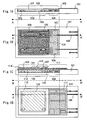
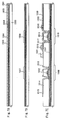
- FIG 1A is a cross-sectional view of a device substrate 101 before semiconductor device is pasted to the device substrate.
- FIG 1B is a top surface view of the device substrate 101 illustrated in FIG 1A.
- FIG 1A is a cross-sectional view of the device substrate 101 illustrated in FIG 1B taken along the line A-A'.
- the device substrate 101 illustrated in FIGS. 1A and 1B has a concave portion 102.
- One or a plurality of LED 103 is provided in the concave portion 102.
- the concave portion 102 can be formed by a known means, for example, a mold.
- the driving of the LED 103 is controlled by a thin film circuit (hereinafter, LED driver thin film circuit) 104 for driving the LED 103.
- the LED driver thin film circuit 104 is not always necessary to be provided in the concave portion 102, that is, the LED driver thin film circuit 104 can be provided except the concave portion 102. The way of forming the LED driver thin film circuit 104 will be described later.
- Reference numeral 105 denotes a wiring formed over the device substrate 101.
- the wiring 105 connects electrically the LED 103 to the LED driver thin film circuit 104, and also connects electrically the LED driver thin film circuit 104 to a semiconductor device pasted later to an exterior of the liquid crystal display apparatus.
- the wiring 105 can be formed over the device substrate 101 by a known means such as plating.
- Reference numeral 106 denotes a reflection film that is formed by depositing metals by vapor deposition in the concave portion 102. To prevent short-circuiting, the reflection film 106 is deposited to be electrically separated from the wiring 105 or the LED 103.
- a reflection film that is formed by vapor deposition is used, however, a reflection plate that is formed separately may be pasted onto the device substrate 101.
- the reflection plate is preferably pasted onto the position so as to reflect light emitted from the LED 103 in the direction of a liquid crystal cell.
- the reflection plate can be provided over surface that is opposing to the LED 103 and that is not provided with the concave portion 102.
- the LED 103 is covered with a resin 107.
- the resin 107 fills the concave portion 102.
- the LED driver thin film circuit 104 is covered with the resin 107.
- the resin 107 known resin such as acrylic resin, epoxy resin, urethane resin, polycarbonate resin, or vinyl resin can be used.
- Transparent particles having different refractive index from that of the resin can be dispersed in the resin 107.
- spherical particles can be dispersed in polymethyl methacrylate resin. It is desired that resin be appropriately selected according to the pasting process of a semiconductor device.
- reference numeral 108 denotes a light source portion that is provided with the LED 103 and the reflection film 106, and that is covered with the resin 107.
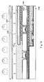
- FIG 1C is a cross-sectional view of the liquid crystal display apparatus according to the invention in which a semiconductor device is pasted and a liquid crystal cell is completed.
- FIG 1D is a top view of the liquid crystal display apparatus illustrated in FIG 1C.
- FIG 1C is a cross-sectional view of FIG 1D taken along the line of B-B'.
- a semiconductor device 110 is pasted to the resin 107 by an adhesive 109. Not shown in FIG 1C, a first polarization plate is provided between the resin 107 and the adhesive 109. In this embodiment, as shown in FIGS. 1C and 1D, the semiconductor device 110 is not only used to a pixel portion of a liquid crystal display apparatus but also used to a thin film circuit 111 for driving or signal processing a liquid crystal display apparatus.
- Reference numeral 113 denotes a counter substrate that is encapsulated with liquid crystal 112 by a sealant 114.
- the region where the liquid crystal 112 is encapsulated by the counter substrate 113 corresponds to a panel 115.
- Light from the light source portion 108 is radiated to a pixel portion 116 provided to the panel 115.
- the thin film circuit 111 is electrically connected to the wiring 105 by wire bonding method, flip chip method, or the like.
- signals or power source voltage can be supplied to a liquid crystal display apparatus via the wiring 105, but not exclusively, signals or power source voltage may be supplied by light using a light-emitting device, a light sensor, or the like, or by electromagnetic induction using an antenna coil.
- a plastic substrate As a plastic substrate, ARTON® containing norbornene resin with polar group by JSR Corporation can be used.
- a plastic substrate such as polyethylene terephthalate (PET), polyether sulfone (PES), polyethylene naphthalate (PEN), polycarbonate (PC), nylon, polyether ether ketone (PEEK), polysulfone (PSF), polyetherimide (PEI), polyalylate (PAR), polybutylene terephthalate (PBT), or polyimide can be used.
- PET polyethylene terephthalate
- PES polyether sulfone
- PEN polyethylene naphthalate
- PC polycarbonate
- PEEK polyether ether ketone
- PSF polysulfone
- PEI polyetherimide
- PAR polyalylate
- PBT polybutylene terephthalate
- polyimide polyimide
- a concave portion is provided to a device substrate and an LED is provided in the concave portion is explained in this embodiment, however, the invention is not limited thereto.
- a flat plastic substrate without concave portion can be used as the device substrate.
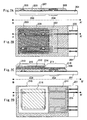
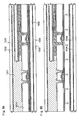
- FIG 2A is a cross-sectional view of a device substrate in which a semiconductor device has not pasted yet.
- the device substrate 201 is flat and not provided with a concave portion.
- FIG 2B is a top view of the device substrate 201 illustrated in FIG 2A.
- FIG 2A is a cross-sectional view of FIG 2B taken along the line A-A'.
- LED driver thin film circuit 204 denotes an LED driver thin film circuit.
- the LED driver thin film circuit 204 is electrically connected to the LED 203 by a wiring 205.
- the wiring 205 is used for electrically connecting the LED driver thin film circuit 204 or a semiconductor device, which is formed later, to exterior of the liquid crystal display apparatus.
- a reflection film 206 is deposited to be separated from the wiring 205 and the LED 203. A reflection film that is formed separately can be used instead of that formed by vapor deposition.
- the LED 203 is covered with a resin 207.
- a photosensitive resin is coated and partly exposed, then, the resin 207 is coated in order to expose a part of the wiring 205.
- the LED driver thin film circuit 204 may also be covered with the resin 207.
- reference numeral 208 denotes a light source portion that is provided with the LED 203 and the reflection film 206, and that is covered with the resin 207.
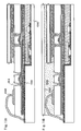
- FIG 2C is a cross-sectional view of a liquid crystal display apparatus according to the invention in which a semiconductor device is pasted and a liquid crystal cell is completed.
- FIG 2D is a top view of the liquid crystal display apparatus illustrated in FIG 2C.
- FIG 2C is a cross-sectional view of FIG 2D taken along the line of B-B'.
- a semiconductor device 210 is pasted onto the resin 207 by an adhesive 209. Not shown in FIG 2C, a first polarization plate is provided between the resin 207 and the adhesive 209.
- reference numeral 211 corresponds to a thin film circuit formed using the semiconductor device 210.
- Reference numeral 213 denotes a counter substrate that is encapsulated with liquid crystal 212 by a sealant 214.
- the region where the liquid crystal 212 is encapsulated by the counter substrate 213 corresponds to a panel 215.
- Light from the light source portion 208 is radiated to a pixel portion 216 provided with the panel 215.
- the thin film circuit 211 is electrically connected to the wiring 205 by wire bonding method, flip chip method, or the like.
- the concave portion of the device substrate allows the LED to be covered with a resin while wiring is exposed by only dropping a resin into the concave portion. Further, a reflection film in the concave portion allows light emitted from LED to radiate effectively to the pixel portion. In case that the concave portion is not provided, the intensity of the device substrate can be further increased compared with the case that the concave portion is provided.
- the semiconductor device included in a thin film circuit and a liquid crystal display apparatus is not limited to the two TFTs, any circuit device can be used.
- a memory device, a diode, a photoelectric conversion device, a resistive element, a coil, a capacitance element, an inductor, or the like can be typically given as examples for the semiconductor device, in addition to TFTs.
- a metal film 501 is deposited over a first substrate 500 by sputtering.
- tungsten is used for forming the metal film 501 and formed to have a thickness of from 10 to 200nm, preferably, from 50 to 75nm.
- the metal film 501 is deposited directly on the first substrate 500, but the metal film 501 may also be deposited after covering the first substrate 500 by an insulating film such as silicon oxide, silicon nitride, silicon oxynitride, or the like.
- An oxide film 502 is deposited to be stacked after depositing the metal film 501 without exposing to the air.
- a silicon oxide film is deposited to have a thickness of from 150 to 300nm as the oxide film 502.
- a film is deposited over the edge of the first substrate 500.
- the metal film 501 and the oxide film 502 are preferably removed selectively by O 2 ashing and the edge of the first substrate 500 is preferably cut by dicing to prevent the oxide film 502 from remaining over the first substrate 500 in separating in a later process.
- pre-sputtering that is, plasma is generated by shielding between a target and a substrate with shutter, is carried out as a preliminary step toward sputtering.
- the first substrate 500 is pre-sputtered under the equilibrium state, that is, Ar flow rate used is 10sccm; O 2 , 30sccm; substrate temperature, 270°C; and deposition power, 3kW.
- a metal oxide film 503 is deposited having an ultra thin thickness of several nm (here, 3nm) between the metal film 501 and the oxide film 502 by the pre-sputtering.
- the metal oxide film 503 is formed by oxidization of the metal film 501.
- the metal oxide film 503 is formed of tungsten oxide.
- the metal oxide film 503 is, but not exclusively, deposited by pre-sputtering in this embodiment.
- the metal oxide film 503 may be deposited by oxidizing deliberately the surface of the metal film 501 in plasma using oxygen or oxygen added with inert gases such as Ar or the like.
- a base film 504 is deposited by plasma chemical vapor deposition (hereinafter, PCVD).
- PCVD plasma chemical vapor deposition
- a silicon oxynitride film is deposited to have a thickness approximately of 100nm as the base film 504.
- a semiconductor film 505 is deposited without exposing to the atmosphere.
- the semiconductor film 505 is formed to have a thickness of from 25 to 100nm, preferably, from 30 to 60nm.
- the semiconductor film 505 may be either an amorphous semiconductor or a polycrystalline semiconductor.
- the semiconductor film may be formed by not only silicon but also silicon germanium. In case of using silicon germanium, the concentration of germanium is preferably approximately from 0.01 to 4.5atomic%.
- the semiconductor film 505 is crystallized by a known technique.
- a known technique thermal crystallization using an electric heating furnace, laser crystallization using a laser light, and ramp annealing crystallization using an infrared light.
- crystallization using catalytic elements can be used according to the technique disclosed in Unexamined Patent Publication No. 7-130652.
- the semiconductor film 505 that is a polycrystalline semiconductor film may be formed in advance by sputtering, PCVD, or thermal CVD.
- the semiconductor film 505 is crystallized by laser crystallization in this embodiment.
- a crystal having a large grain diameter can be obtained by laser light irradiation of from a second harmonic to a fourth harmonic of a fundamental wave by using a solid laser capable of continuously oscillating.
- a second harmonic (532nm) or a third harmonic (355nm) of Nd: YVO 4 laser (fundamental wave of 1064nm) may be applied.
- a continuously oscillating laser is used, a laser light emitted from the continuously oscillating YVO 4 laser having an output power of 10W is converted to a harmonic by a nonlinear optical device.
- a harmonic is outputted by using nonlinear optical device.
- the laser light is formed by using an optical system such that it becomes in a rectangular shape or an elliptical shape on an irradiating face and radiated to the semiconductor film 505.
- the laser irradiation is carried at energy density of approximately from 0.01 to 100MW/cm 2 (preferably from 0.1 to 10MW/cm 2 ) and a scanning speed of approximately from 10 to 2000 cm/s.
- the laser crystallization may be carried out by radiating a continuous wave laser light of fundamental wave and a continuous wave laser light of harmonic wave, or radiating a continuous wave laser light of fundamental wave and a pulsed laser light of harmonics.
- a laser light may be radiated in an inert gas atmosphere such as rare gas or nitride. According to this, the surface roughness of a semiconductor due to a laser irradiation, further, the variations of a threshold value due to the variations of interface state density can be prevented.
- a semiconductor film 506 that is enhanced its degree of crystallinity is formed by irradiating the above described semiconductor film 505 with a laser light.
- the semiconductor film 506 is patterned to form island like semiconductor films 507, 508.
- Various semiconductor devices as typified by TFTs are formed using the island like semiconductor films 507, 508.
- the base film 504 and the island like semiconductor films 507, 508 are in contact with each other, but an electrode, an insulating film, or the like may be formed between the base film 504 and the island like semiconductor films 507, 508 depending on a semiconductor device.
- a gate electrode and a gate insulating film are formed between the base film 504 and the island like semiconductor films 507,508.
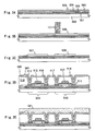
- top gate type TFTs 509 and 510 are formed using the island like semiconductor films 507, 508 (FIG. 3D). Specifically, a gate insulating film 511 is deposited so as to cover the island like semiconductor films 507, 508. Then, a conductive film is deposited over the gate insulating film 511 and patterned, and gate electrodes 512, 513 are formed. Next, impurities imparting n-type are added to the island like semiconductor films 507, 508 using the gate electrodes 512, 513 or resist that is deposited and patterned as masks to form a source region, a drain region, and an LDD (Lightly Doped Drain) region.
- TFTs 509, 510 are n-type, in case of using p-type TFTs, impurities imparting p-type are added.
- TFTs 509, 510 can be formed.
- a method for manufacturing the TFTs is not limited to the above described process.
- a first interlayer insulating film 514 is fabricated so as to cover the TFTs 509, 510.
- Contact holes are formed at the gate insulating film 511 and the first interlayer insulating film 514, and terminals 515 to 518 connected to the TFTs 509, 510 via the contact holes are formed so as to be in contact with the first interlayer insulating film 514.
- a pixel electrode 540 of a liquid crystal cell is formed by a transparent conductive film such as ITO so as to be in contact with the terminal 515. Then, an orientation film 541 is formed to cover the pixel electrode 540, and rubbing treatment is carried out to the orientation film 541. A part of the terminal 518 is exposed by etching or the like so as not to be covered by the orientation film 541.
- a protective layer 521 is formed over the orientation film 541.
- a material for forming the protective layer 521 a material which can protect the surface of the TFTs 509, 510, the orientation film 541, and terminals 515 to 518 in pasting or separating the second substrate in a later process, and which can be removed after separating a second substrate is used.
- the protective film 521 can be formed by coating resin of epoxy series, acrylate series, or silicon series that is soluble in water over the whole surface, and baking.
- a water-soluble resin (TOAGOSEI Co., Ltd.: VL-WSHL10) is spin-coated to have a thickness of 30 ⁇ m, and exposed for two minutes to be partially cured, then, exposed its back with UV rays for 2.5 minutes, and then, exposed its surface for 10 minutes, that is, 12.5 minutes in total, to be fully cured. Consequently, the protective layer 521 is formed (FIG 3E).
- the orientation film 541 may be formed after removing the protective layer 521 in a later process.
- the orientation film 541 may be formed after removing the protective layer 521 in a later process.
- an inorganic insulating film (a SiN X film, a SiN X O Y film, an AlN x film, or an AlN X O Y film) is preferably formed so as to cover the first interlayer insulating film 514, and be disposed between the first interlayer insulating film 514 and the terminals 515 to 518 for removing smoothly the protective film 521 in a later process.
- the metal oxide film 503 is crystallized. By this crystallization, the metal oxide film 503 becomes susceptible to fracture in grain boundary and enhanced its brittleness.
- the crystallization is carried out by heat-treating for approximately at from 420 to 550°C for from 0.5 to 5 hours.
- some treatments are carried out on the metal oxide film 503 in order to make it easier for the metal oxide film 503 to be separated by weakening partly the adhesiveness between the metal oxide film 503 and the oxide film 502 or the adhesiveness between the metal oxide film 503 and the metal film 501.
- the periphery of the region that is to be separated is locally pressed from outside to be damaged a part of the inside or the boundary face-neighborhood of the oxide film 503.
- a hard needle such as a diamond pen is attached perpendicular to the edge-neighborhood of the metal oxide film 503 and moved along with the metal oxide film 503 with applying loading.
- a scriber device can be used to move with applying loading on the region with press force ranging from 0.1 to 2mm. It is important to carry out some treatment for easy separating, that is, it is important to prepare for separating process. Such preparatory process to weaken selectively the adhesiveness will prevent poor separating and improve the process yield.
- a second substrate 523 is pasted onto the protective film 521 with a two-sided tape 522, and a third substrate 525 is pasted over the first substrate 500 with a twp-sided tape 524 (FIG 4A).
- An adhesive can be used instead of a two-sided tape. For example, it is possible to reduce the load of a semiconductor device, which becomes increased by separating the second substrate, by using an adhesive that is melted with UV light.
- the third substrate 525 prevents the first substrate 500 from being damaged in a later process for separating.
- the substrate that has higher rigidity than that of the first substrate 500 for example, a quartz substrate or a semiconductor substrate is preferably to be used.
- the metal film 501 is separated from the oxide film 502 by a physical means.
- the separation of metal film 501 is started from the region that is partly weakened its adhesiveness to the metal film 501 or the oxide film 502 in the previous process.
- the metal film 501 may be removed by separating the metal film 501 from metal oxide film 503, by separating the oxide film 502 from the metal oxide film 503, or splitting the metal oxide film 503 into two. Further, the second substrate 523 to which semiconductor devices (here, TFTs 509, 510) are pasted is separated from the third substrate 525 to which the first substrate 500 and the metal film 501 are pasted. The separation can be carried out with comparatively small force (for example, man's hand, air pressure of gas sprayed from a nozzle, ultrasonic waves, or the like).
- FIG 4B shows a state of after separating.
- a first polarization plate 527 provided over a resin 533 is bonded to the oxide layer 502 that is partly attached with the metal oxide film 503 with an adhesive 526 (FIG 4C).
- the material for the adhesive 526 is selected in order that the adhesiveness between the oxide layer 502 and the first polarization plate 527 by the adhesive 526 to be stronger than that between the second substrate 523 and the protective layer 521 by the two-sided tape 522.
- the adhesiveness of the polarization plate 527 may get worse, so that the remained metal oxide film may be completely removed before bonding to the oxide film 502.
- the semiconductor devices 509, 510 are used for the thin film circuit, the semiconductor devices 509, 510 are unnecessary to be pasted to overlap with the first polarization plate 527.
- the adhesive 526 various curing adhesives such as a photo-curing adhesive, for example, a reaction-curing adhesive, a thermal-curing adhesive, or a UV-curing adhesive, or an anaerobic adhesive can be used. More preferably, the adhesive 526 is given high thermal conductivity by means of mixing powder comprising silver, nickel, aluminum, or aluminum nitride, or filler.
- reference numeral 530 denotes a wiring formed over the device substrate 534.
- the wiring 530 is formed by coating copper with solder, gold, or tin.
- the two-sided tape 522 and the second substrate 523 are separated sequentially or simultaneously from the protective layer 521.
- the two-sided tape 522 can be separated simultaneously with curing the adhesive 526 by using UV-curing adhesive as the adhesive 526, and by using a tape or adhesive that is separated by UV light as the two-sided tape 522.
- the protective film 521 is removed by water since the protective film 521 is formed by a resin that is soluble in water.
- the remained protective film 521 is preferably removed by carrying out cleaning treatment or O 2 plasma treatment to the surface.
- tungsten is used for a material of the metal film 501, however, the present invention is not limited thereto. Any material can be used as long as which includes metals that allows a substrate to be separated by forming the metal oxide film 503 over the surface of the material and crystallizing the metal oxide film 503. For instance, TiN, WN, Mo, or the like can be used in addition to tungsten.
- the optimal temperature for heat treatment to crystallize differs depending on the composition ratio of the metal film. On the basis of the fact, the heat treatment can be carried out at the temperature that has no adverse effects on the manufacturing process for a semiconductor device, and selection ranges of the manufacturing process become difficult to be restricted by adjusting the composition ratio of the metal film.
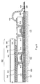
- a liquid crystal cell is formed as illustrated in FIG 6.
- a counter substrate 542 that is formed separately is pasted with sealant 543. Filler may be mixed into the sealant.
- the counter substrate 542 has a thickness of approximately several hundreds ⁇ m, and is provided with a counter electrode 543 formed by a transparent conductive film and an orientation film 544 that is rubbing treated.
- a color filter and a black matrix (a shielding film) to prevent disclination may be formed.
- a second polarization plate 545 is pasted onto the opposite side of the counter electrode 543 on which the counter substrate 542 is formed.
- liquid crystal 546 is injected and encapsulated to complete a panel 550.
- the way of injecting liquid crystal may be dispenser method or dip method.
- a spacer may be provided between the pixel electrode 540 and the counter electrode 543 for keeping cell gaps.
- the liquid crystal display apparatus is completed by connecting electrically the terminal 518 to the wiring 530 provided with the device substrate 534 by wire bonding method.
- a method for manufacturing a liquid crystal display apparatus according to the invention which is different from that illustrated in FIGS. 3 to 6, will be explained.
- a TFT is exemplified as the semiconductor device
- the semiconductor device included in a thin film circuit and a liquid crystal display apparatus is not limited to the TFT, any circuit device can be used.
- a memory device, a diode, a photoelectric conversion device, a resistive element, a coil, a capacitance element, an inductor, or the like can be typically given, in addition to TFTs.
- a metal film 1501 is deposited over a first substrate 1500 by sputtering.
- tungsten is used for forming the metal film 1501 and formed to have a thickness of from 10 to 200nm, preferably, from 50 to 75nm.
- the metal film 1501 is deposited directly on the first substrate 1500, but the metal film 1501 may also be deposited after covering the first substrate 1500 by an insulating film such as silicon oxide, silicon nitride, silicon oxynitride, or the like.
- An oxide film 1502 composing the insulating film is deposited to be stacked after depositing the metal film 1501 without exposing to the air.
- a silicon oxide film is deposited to have a thickness of from 150 to 300nm as the oxide film 1502.
- a film is deposited over the edge of the first substrate 1500.
- the metal film 1501 and the oxide film 1502 are preferably removed selectively by O 2 ashing to prevent the oxide film 1502 from remaining over the first substrate 1500 in separating in a later process.
- pre-sputtering that is, plasma is generated by shielding between a target and a substrate with shutter, is carried out as a preliminary step toward sputtering.
- the first substrate 1500 is pre-sputtered under the equilibrium state, that is, Ar flow rate used is 10sccm; O 2 , 30sccm; substrate temperature, 270°C; and deposition power, 3kW.
- a metal oxide film 1503 is deposited having an ultra thin thickness of several nm (here, 3nm) between the metal film 1501 and the oxide film 1502 by the pre-sputtering.
- the metal oxide film 1503 is formed by oxidization of the metal film 1501. Hence, the metal oxide film 1503 is formed of tungsten oxide.
- the metal oxide film 1503 is, but not exclusively, deposited by pre-sputtering in this embodiment.
- the metal oxide film 1503 may be deposited by oxidizing deliberately the surface of the metal film 1501 in plasma using oxygen or oxygen added with inert gases such as Ar or the like.
- a base film 1504 composing the insulating film is deposited by PCVD.
- a silicon oxynitride film is deposited to have a thickness of approximately 100nm as the base film 1504.
- a semiconductor film 1505 is deposited without exposing to the atmosphere.
- the semiconductor film 1505 is formed to have a thickness of from 25 to 100nm, preferably, from 30 to 60nm.
- the semiconductor film 1505 may be either an amorphous semiconductor or a polycrystalline semiconductor.
- the semiconductor film may be formed by not only silicon but also silicon germanium. In case of using silicon germanium, the concentration of germanium is preferably approximately from 0.01 to 4.5atomic%.
- the semiconductor film 1505 is crystallized by a known technique.
- a known technique thermal crystallization using an electric heating furnace, laser crystallization using a laser light, and ramp annealing crystallization using an infrared light.
- crystallization using catalytic elements can be used according to the technique disclosed in Unexamined Patent Publication No. 7-130652.
- the semiconductor film 1505 is crystallized by laser crystallization in this embodiment. Before the laser crystallization, the semiconductor film is thermal-annealed at 500°C for 1 hour to increase resistance of the semiconductor film to laser. In this embodiment, the heat treatment enhances the brittleness of the metal oxide film 1503 to make it easier for the first substrate 1500 to be separated later. By this crystallization, the metal oxide film 1503 becomes susceptible to fracture in grain boundary and enhanced its brittleness.
- the crystallization of the metal oxide film 1503 is preferably carried out by heat-treating for approximately at from 420 to 550°C from 0.5 to 5 hours.
- a crystal having a large grain diameter can be obtained by laser light irradiation of from a second harmonic to a fourth harmonic of a fundamental wave by using a solid laser capable of continuously oscillating.
- a second harmonic (532nm) or a third harmonic (355nm) of Nd: YVO 4 laser (fundamental wave of 1064nm) may be applied.
- a continuously oscillating laser is used, a laser light emitted from the continuously oscillating YVO 4 laser having an output power of 10W is converted to a harmonic by a nonlinear optical device.
- a harmonic is outputted by using a nonlinear optical device.
- the laser light is formed by using an optical system such that it becomes in a rectangular shape or an elliptical shape when radiated to an irradiating face, and radiated to the semiconductor film 1505.
- an energy density of approximately from 0.01 to 100MW/cm 2 preferably from 0.1 to 10MW/cm 2
- a semiconductor film may be irradiated with the laser light while it is moved relatively thereto at a speed of approximately from 10 to 2000 cm/s.
- the laser crystallization may be carried out by radiating a continuous wave laser light of fundamental wave and a continuous wave laser light of harmonic wave, or radiating a continuous wave laser light of fundamental wave and a pulsed laser light of harmonics.
- a laser light may be radiated in the inert gas atmosphere such as rare gas or nitride. According to this, the surface roughness of a semiconductor due to a laser irradiation, further, the variations of a threshold value due to the variations of interface state density can be prevented.
- the crystallinity of the semiconductor film 1505 is further enhanced by the above described crystallization.
- the semiconductor film 1505 that is a polycrystalline semiconductor film may be formed in advance by sputtering, PCVD, thermal CVD, or the like.
- the semiconductor film 1505 is patterned to form island like semiconductor films 1507, 1508.
- Various semiconductor devices as typified by TFTs are formed using the island like semiconductor films 1507, 1508.
- the base film 1504 and the island like semiconductor films 1507, 1508 are in contact with each other, but an electrode, an insulating film, or the like may be formed between the base film 1504 and the island like semiconductor films 1507, 1508 depending on a semiconductor device.
- a gate electrode and a gate insulating film are formed between the base film 1504 and the island like semiconductor films 1507, 1508.
- top gate type TFTs 1509, 1510 are formed using the island like semiconductor films 1507, 1508 (FIG 7C). Specifically, a gate insulating film 1511 is deposited so as to cover the island like semiconductor films 1507, 1508. Then, a conductive film is deposited over the gate insulating film 1511 and patterned, and then, gate electrodes 1512, 1513 are formed. Next, impurities imparting n-type are added to the gate electrodes 1507, 1508 using the gate electrodes 1512, 1513 or resist that is deposited and patterned as masks to form a source region, a drain region, and an LDD (Lightly Doped Drain) region.
- TFTs 1509, 1510 are n-type, but impurities imparting p-type are added in case of using p-type TFTs.
- TFTs 1509, 1510 can be formed.
- a method for manufacturing the TFTs is not limited to the above described process.
- a first interlayer insulating film 1514 is fabricated so as to cover the TFTs 1509, 1510. Contact holes are formed in the gate insulating film 1511 and the first interlayer insulating film 1514, and terminals 1515 to 1518 connected to the TFTs 1509, 1510 via the contact holes are formed so as to be in contact with the first interlayer insulating film 1514.
- the TFT 1510 used as a switching element of the pixel portion of the liquid crystal display apparatus is electrically connected to the terminal 1518.
- a pixel electrode of a liquid crystal cell is formed by transparent conductive film such as ITO so as to connect to the terminal 1518.
- a spacer 1519 is formed by using an insulating film.
- an orientation film 1520 is formed to cover the pixel electrode 1550, the terminal 1518, and the spacer 1519, and rubbing treatment is carried out thereto.
- the orientation film 1520 may be formed to overlap with the thin film circuit.
- a sealant 1521 is formed to encapsulate liquid crystal.
- liquid crystal 1522 is dropped in the region encircled by the sealant 1521.
- a counter substrate 1523 that is formed separately is pasted with sealant 1521.
- FIG 8B is a view showing a state after the counter substrate 1523 is pasted. Filler may be mixed into the sealant 1521.
- the counter substrate 1523 has a thickness of approximately several hundreds ⁇ m, and is provided with a counter electrode 1524 formed by a transparent conductive film and an orientation film 1526 that is rubbing treated.
- a color filter and a black matrix (a shielding film) to prevent disclination may be formed.
- a second polarization plate 1527 is pasted onto the opposite side of the counter electrode 1524 on which the counter substrate 1523 is formed.
- the region where the counter electrode 1524, the liquid crystal 1522, and the pixel electrode 1550 are overlapped each other corresponds to a liquid crystal cell 1528.
- a panel 1529 is also completed.
- a thin film circuit 1530 is not overlapped with the counter substrate 1523, the thin film circuit 1530 may dare to be overlapped with the counter substrate 1523.
- a resin may be filled between the counter substrate and the thin film circuit to increase mechanical strength of a liquid crystal display apparatus.
- the liquid crystal is encapsulated by dispenser method (dropping method) though, the invention is not limited thereto.
- the liquid crystal may be encapsulated by dipping method (pumping method) utilizing capillary phenomenon after pasting the counter substrate onto the liquid crystal.
- a protective film 1531 is formed to cover the thin film circuit 1530 and the panel 1529.
- the protective layer 1531 is formed by a material that can protect the thin film circuit 1530 and the panel 1529 in pasting or separating a second substrate 1533 later, and that can be removed after separating the second substrate 1533.
- the protective film 1531 can be formed by coating resin of epoxy series, acrylate series, or silicon series that is soluble in water over the whole surface.
- a water-soluble resin (TOAGOSEI Co., Ltd.: VL-WSHL10) is spin-coated to have a thickness of 30 ⁇ m, and exposed for two minutes to be partially cured, then, exposed its back with UV rays for 2.5 minutes, and then, exposed its surface for 10 minutes to be fully cured. Consequently, the protective layer 1531 is formed.
- an inorganic insulating film (a SiN X film, a SiN X O Y film, an AlN X film, or an AlN X O Y film) is preferably formed so as to cover the first interlayer insulating film 1514.
- some treatments are carried out on the metal oxide film 1503 in order to make it easier for the metal oxide film 1503 to be separated by weakening partly the adhesiveness between the metal oxide film 1503 and the oxide film 1502 or the adhesiveness between the metal oxide film 1503 and the metal film 1501.
- the periphery of the region that is to be separated is locally pressed from outside to damage a part of the inside or the boundary face-neighborhood of the oxide film 1503.
- a hard needle such as a diamond pen is attached perpendicular to the edge-neighborhood of the metal oxide film 1503 and moved along with the metal oxide film 1503 with applying loading.
- a scriber device can be used to move with applying loading on the region with press force ranging from 0.1 to 2mm. It is important to carry out some treatment for easy separating, that is, it is important to prepare for separating. Such preparatory process to weaken selectively the adhesiveness will prevent poor separating and improve the process yield.
- a second substrate 1533 is pasted onto the protective layer 1531 with a two-sided tape 1532, and a third substrate 1535 is pasted over the first substrate 1500 with a two-sided tape 1534.
- An adhesive can be used instead of a two-sided tape.
- the third substrate 1535 prevents the destruction of the first substrate 1500 in the subsequent process of separating.
- the substrate that has higher rigidity than that of the first substrate 1500 for example, a quartz substrate or a semiconductor substrate is preferably to be used.
- the metal film 1501 is separated from the oxide film 1502 by a physical means.
- the separation of metal film 1501 is started from the region that is partly weakened its adhesiveness with respect to the metal film 1501 or the oxide film 1502 in the previous process.
- Three separating portions may be resulted from the separation of metal film 1501, that is, the separating portion of the metal film 1501 and metal oxide film 1503, the separating portion of the oxide film 1502 and the metal oxide film 1503, or the separating portion within the metal oxide film 1503.
- the second substrate 1533 on which semiconductor devices (here, TFTs 1509, 1510) are pasted is separated from the third substrate 1535 on which the first substrate 1500 and the metal film 1501 are pasted.
- the separation can be carried out with comparatively small force (for example, man's hand, air pressure of gas sprayed from a nozzle, ultrasonic waves, or the like).
- FIG 9B shows a state of after the separating process.
- a device substrate 1540 is bonded with an adhesive 1539 to the oxide layer 1502 that is partly attached with the metal oxide film 1503 (FIG 10).
- the material for the adhesive 1539 is selected in order that the adhesiveness to be stronger between the oxide layer 1502 and the device substrate 1540 by the adhesive 1539 than that between the second substrate 1533 and the protective layer 1531 by the two-sided tape 1532.
- the adhesive 1539 various curing adhesives such as a photo-curing adhesive, for example, a reaction-curing adhesive, a thermal-curing adhesive, or a UV-curing adhesive, or an anaerobic adhesive can be used. More preferably, the adhesive 1539 is given high thermal conductivity by means of mixing powder comprising silver, nickel, aluminum, or aluminum nitride, or filler.
- the adhesiveness of the device substrate 1540 may get worse, so that the remained metal oxide film may be completely removed by etching or the like before bonding to a printed wiring board.
- the two-sided tape 1532 and the second substrate 1533 are separated sequentially or simultaneously from the protective layer 1531.
- the two-sided tape 1532 can be separated simultaneously with curing the adhesive 1539 by using UV-curing adhesive as the adhesive 1539, and by using a tape or adhesive that is separated by UV light as the two-sided tape 1532.
- the protective film 1531 is removed by water since the protective film 1531 is formed by a resin that is soluble in water.
- the remained protective film 1531 is preferably removed by carrying out cleaning treatment or O 2 plasma treatment to the surface.
- a terminal 1518, a wiring 1551 provided with the device substrate 1540 are electrically connected each other by a wiring 1552 by wire bonding method, and a liquid crystal display apparatus is completed.
- the wiring 1551 is completed, for example, by coating copper with gold or tin.
- a timing for connecting the terminal 1518 and the wiring 1551 is not limited to the above described one.
- liquid crystal display apparatus is completed in this state.
- mechanical strength of the liquid crystal display apparatus is enhanced by encapsulating the liquid crystal display apparatus by a sealing member.
- the thin film circuit 1530 and the panel 1529 are covered with a resin 1542 and a cover member 1543 is provided to protect the thin film circuit 1530 and the panel 1529.
- the cover member 1543 is not always necessary to be provided, the device substrate 1540 can be covered directly with a sealing member.
- material for the sealing member used for encapsulating the liquid crystal display apparatus a material that is used in general can be used.
- polymeric material such as polyester, acrylic acid, polyvinyl acetate, propylene, chloroethene, acrylonitrilebutadiene styrene resin, or polyethylene terephthalate can be used.
- the pixel portion of the liquid crystal display apparatus is exposed, or a material for the resin 1542 or a cover member 1543 is appropriately selected in encapsulating in order to pass light therethrough.
- a plastic substrate can be used for the device substrate 1540, the cover member 1543, and the counter substrate 1523.
- a plastic substrate ARTON® containing norbornene resin with polar group by JSR Corporation can be used.
- a plastic substrate such as polyethylene terephthalate (PET), polyether sulfone (PES), polyethylene naphthalate (PEN), polycarbonate (PC), nylon, polyether ether ketone (PEEK), polysulfone (PSF), polyetherimide (PEI), polyalylate (PAR), polybutylene terephthalate (PBT), or polyimide can be used.
- PET polyethylene terephthalate
- PES polyether sulfone
- PEN polyethylene naphthalate
- PC polycarbonate
- PEEK polyether ether ketone
- PSF polysulfone
- PEI polyetherimide
- PAR polyalylate
- PBT polybutylene terephthalate
- the device substrate 1540
- tungsten is used for a material of the metal film 1501, however, the present invention is not limited thereto. Any material can be used as long as which includes metals that allows a substrate to be separated by forming the metal oxide film 1503 over the surface of the material and crystallizing the metal oxide film 1503. For instance, TiN, WN, Mo, or the like can be used in addition to tungsten.
- the optimal temperature for heat treatment to crystallize differs depending on the composition ratio of the metal film. On the basis of the fact, the heat treatment can be carried out at the temperature that has no adverse effects on the manufacturing process for a semiconductor device, and selection ranges of the manufacturing process become difficult to be restricted by adjusting the composition ratio of the metal film.
- a semiconductor device used for an LED driver thin film circuit can be formed according to the above described method for forming a semiconductor device.
- a material for a resin covering a light-emitting diode is preferably and appropriately selected depending on the method for curing a first substrate, a second substrate, and an adhesive.
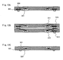
- FIG. 12A is a cross-sectional view of a thin film circuit or an LED driver thin film circuit, each of which is provided with solder balls.
- a semiconductor device 301 is electrically connected to a wiring over a device substrate with a solder ball 302.
- the solder ball 302 is provided to the side of the device substrate of the semiconductor device 301 and connected to an electrode 303 that is electrically connected to the semiconductor device 301.
- the electrode 303 may be formed by a conductive film that is the same as that of a gate electrode of a TFT in case that the semiconductor device is the TFT.
- FIG 12B is a cross-sectional view of the thin film circuit or the LED driver thin film circuit in which semiconductor devices are stacked by flip chip method.
- semiconductor devices 310 and 311 each of which is provided to two layers, are stacked.
- a wiring provided to a device substrate is electrically connected to the semiconductor device 310 with a solder ball 312.
- the semiconductor device 310 is electrically connected to the semiconductor device 311 with a solder ball 313.
- FIG 12C is a view showing an example that a wiring formed over a device substrate is connected to a solder ball. As shown in FIG. 12C, a solder ball 312 is connected to a wiring 321 directly connected to a semiconductor device 320.
- flip chip method is effective for the case that the number of connections between a thin film circuit or an LED driver thin film circuit and a wiring is large, since a pitch between wirings can be relatively reserved large compared with wire bonding method.
- a solder ball and a wiring over a device substrate can be connected by various methods such as thermo-compression bonding and thermo-compression bonding with vibrations from ultrasonic wave.
- An under fill may fill interspace of thermo-compressed solder balls between each other to improve the mechanical strength of connection portions or the efficiency of radiation of heat generated in a thin film circuit.
- An under fill is not always necessary to be used, but it can prevent poor connection due to stress occurred by mismatch of coefficient of thermal expansion of a device substrate and a semiconductor device.
- the compression by applying ultrasonic wave can prevent poor connection compared with compression without ultrasonic wave. Especially, it is effective for the case that the number of bumps used for connecting is at least approximately 300.
- a wiring formed over a device substrate can be electrically connected to a thin film circuit or an LED driver thin film circuit in various forms by combining the ways described with reference to FIGS. 12A to 12C.
- a flip chip method and wire bonding method can be combined for connecting.
- a liquid crystal display apparatus can be drastically reduced its thickness and weight without being damaged the mechanical strength.
- Applying a liquid crystal display apparatus according to the invention to an electronic appliance a space for using IC can be kept large and an electronic appliance can be sophisticated without preventing the electronic appliance from being lightweight and downsized.
- a liquid crystal display apparatus according to the present invention is useful for a portable electronic appliance since usability thereof becomes improved by reducing the weight and the size. According to the invention, even when size of a pixel portion of a liquid crystal display apparatus is increased, weight thereof is almost the same as that of a liquid crystal display apparatus using a conventional glass substrate.
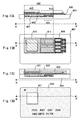
- FIG. 13A is a cross-sectional view showing a device substrate 401 at the time that a panel is completed.
- FIG 13B is a top surface view of the device substrate illustrated in FIG 13A.
- FIG 13A shows the state that is taken along the line of A-A'.
- the device substrate 401 illustrated in FIGS. 13A and 13B has a concave portion 402 in which an LED 403 or a plurality of those is formed.
- An LED driver thin film circuit 404 is provided to the concave portion 402.
- the LED 403 and the LED driver circuit are covered with a resin 407.
- Reference numeral 415 denotes a panel
- 411 denotes a thin film circuit.
- the panel and the thin film circuit are formed separately and pasted onto the device substrate 401.
- the thin film circuit 411 has an antenna coil 406.
- a wiring 405 formed over the device substrate 401 is connected electrically to the antenna coil 406.
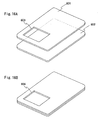
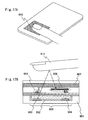
- FIG 13C is a cross-sectional view of a liquid crystal display apparatus according to the invention at the time of completing an electronic card.
- FIG 13D is a top view showing a liquid crystal display apparatus illustrated in FIG 13C.
- FIG 13C is a cross-sectional view showing FIG 13D taken along the line B-B'.
- FIGS. 13C and 13D An electronic card as illustrated in FIGS. 13C and 13D is covered with a cover member 420 so as to seal the panel 415 and the thin film circuit 411 formed over the device substrate with a resin 422.
- the cover member can be formed of a material that is transparent to light in order that light emitted from panel 415 also passes through the area except the portion 421.
- the structure of an electronic card that supplies signal or power supply voltage by electromagnetic introduction using an antenna coil is explained, however, the electronic card can have the structure that supplies signal or power supply voltage by light using a light-emitting device or light sensor. Further, the electronic card is not limited to a noncontact card.
- the electronic card may be a contact card that transmits directly signals to a terminal device via a terminal.
- the electronic card can be used for various purposes such as a cash card, a credit card, a prepaid card, an ID card used for identification, and a commuter pass. If an electronic card is installed with the liquid crystal display apparatus according to the invention, data of the electronic card can be displayed on a pixel portion. Further, the reliability of certification of identity can be improved by displaying a photograph of a face. If a photograph of a face is used instead of a picture for identity, resolution of at least approximately QVGA (320 x 240) is required.
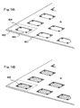
- FIGS. 14A and 14B A method for manufacturing a plurality of liquid crystal display apparatus from a large sized device substrate will be explained with reference to FIGS. 14A and 14B.
- FIGS. 14A and 14B in case of using a large sized device substrate 601, a plurality of concave portions 603 is formed in areas 602, each of which is corresponding to each liquid crystal display apparatus. LEDs 604 are provided in each concave portion 603. A wiring connected electrically to the LED 604, an LED driver thin film circuit, a reflection film, or the like (all are not shown) are provided with the LEDs, and a resin 605 is filled with each concave portion 603 as shown in FIG 14B.
- a panel or a thin film circuit is formed and diced in accordance with the method explained in the embodiment, and a plurality of liquid crystal display apparatus can be manufactured from one device substrate.
- the dicing can be carried out either before or after forming the panel or the thin film circuit.
- an LED is connected to a flexible printed wiring board (FPC) and the FPC is connected to a wiring over a device substrate, instead that the LED is directly connected to the wiring over a device substrate.
- FPC flexible printed wiring board
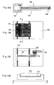
- FIG 15A is a top surface view of an FPC connected with an LED.
- An LED 701 is connected to a lead 702 that is sandwiched by a plastic film 703.
- a terminal 704 connected with the lead 702 is not covered with the plastic film 703 and is exposed.
- FIG 15B is a view showing the state that the LED 701 illustrated in FIG 15A is pasted onto a concave portion 705 in the device substrate 706.
- FIG. 15C is a view showing a reverse side of the device substrate 706 illustrated in FIG 15B.
- a wiring 707 is provided with a reverse side of the concave portion 705.
- the LED 701 provided in the concave portion 705 and the wiring 707 are electrically connected each other by the lead 702.
- the surface of the device substrate 706 provided with the wiring 707 has a concave portion 710.
- the regions provided with the concave portions 705, 710 are preferably not overlapped each other considering the intensity of the device substrate 706.
- a solar cell 708 and a driver circuit 709 for controlling the driving of the solar cell 708 are provided in the concave portion 710.
- the wiring 707 is electrically connected to the driver circuit 709.
- devices that are provided with both sides of the device substrate are electrically connected each other.
- the device substrate can be utilized without waste.
- FIG 15D is a cross-sectional view of the concave portion 705 taken along the dotted line A-A'.
- a metal reflection film 711 is deposited over the surface of the concave portion 711. According to this example, microscopic irregularities are formed on the surface of the reflection film 711 by corroding and by sandblasting using emery, and light emitted from the LED can be diffusely reflected and emitted evenly to the pixel portion.
- FIG 16A is a view showing a plastic substrate 801 having an opening portion 803 and a plastic substrate 802 that is planarized.
- the plastic substrates 801 and 802 are pasted each other.
- a device substrate 805 having a concave portion 804 is formed in the region where the opening portion 803 overlaps with the plastic substrate 802 that is planarized.
- An example that an area sensor is provided with an electronic card utilizing a liquid crystal display according to the present invention.
- FIG 17A is a view showing that a tip of a finger presses a pixel portion 910 that serves not only as an image display portion but also as an area sensor.
- FIG 17B is a view showing a cross-sectional view of the pixel portion 910 illustrated in FIG 17A.
- a device substrate 901 is formed to have a concave portion 905.
- a reflection film 902 is formed over the surface of the concave portion 905.
- An LED 903 is provided in the concave portion 905 and covered with a resin 904.
- a TFT 906 for applying voltage to a liquid crystal 907 and a photo diode 908 are provided over the device substrate 901.
- the TFT 906 and the photo diode 908 are separately formed over different substrates, and separated to paste onto the device substrate 901.
- a liquid crystal display apparatus can be utilized for various electronic appliances. Especially, it is effective to use the liquid crystal display apparatus for portable type electronic appliances since the usability thereof is drastically improved by reducing the weight or the size.
- FIG. 18A is a view showing a sheet-shaped cellular phone comprising a main body 2101, a display unit 2103, a sound input unit 2104, a sound output unit 2105, a switch 2106, an external connection port 2107, or the like.
- An earphone 2108 prepared separately can be connected to the cellular phone via the external connection port 2107.
- a touch panel liquid crystal display apparatus having a sensor according to the present invention is used for the display unit 2103.
- a continuous stream of operation can be carried out by touching a touch panel operation key 2109 displayed on the display unit 2103.
- a thin film circuit provided with the liquid crystal display apparatus according to the invention can be used as various signal processing circuits provided in the main body 2101.
- FIG 18B is a view showing an electronic book comprising a main body 2201, a display unit 2202, an operation key 2203, and the like.
- the main body 2201 can have a built-in modem.
- a liquid crystal display apparatus having a sensor according to the present invention is used for the display unit 2202.
- a thin film circuit provided with the liquid crystal display apparatus according to the invention can be used as various signal processing circuits.
- FIG 18C is a view showing a wrist watch comprising 2301, a display unit 2302, a fastening 2303, and the like.
- a liquid crystal display apparatus having a sensor according to the present invention is used for the display unit 2302.
- a thin film circuit provided with the liquid crystal display apparatus according to the invention can be used as various signal processing circuits provided in the main body 2301.
- FIG 18D is a view showing a personal computer comprising a main body 2401, a display unit 2402, a touch panel key board 2403, a mouse 2404, an external connection port 2405, a power source plug 2406, and the like.
- a liquid crystal display apparatus having a sensor according to the present invention is used for the display unit 2402.
- a touch panel liquid crystal display apparatus having a sensor according to the present invention is used for the touch panel keyboard 2403 and the mouse 2404.
- a continuous stream of operation can be carried out by touching the touch panel key board 2403 and the mouse 2404.
- a thin film circuit provided with the liquid crystal display apparatus according to the invention can be used as various signal processing circuits.
- FIG 18E is a view showing a front glass viewing from the inside of a car.
- a front glass 2501 is pasted with a liquid crystal display apparatus 2503 according to the present invention.
- a display unit 2502 can display various pieces of information required by a driver.
- FIG 18E an example that the liquid crystal display apparatus according to the invention is pasted onto the front glass is explained, but the liquid crystal display apparatus can be pasted onto a window glass of side and back of a driver's seat. Further, the liquid crystal display apparatus can be pasted onto either inside or outside of a car.
- FIG 18F is a view showing an electronic card comprising a main body 2601, a display unit 2602, a connection terminal 2603, and the like.
- the pixel portion of the liquid crystal display apparatus according to the invention can be utilized as the display unit 2602.
- a thin film circuit provided with the liquid crystal display apparatus according to the invention can be used as various signal processing circuits provide in the main body 2601.
- the electronic appliances described in this embodiment can use any structure of liquid crystal structures described in Embodiments 1 to 5.
- a measurement result of a first substrate side after separating and a cross-section of an insulating film side by TEM will be described in this example.
- a W film is deposited to have a thickness of 50nm by sputtering
- a silicon oxide film is deposited to have a thickness of 200nm by sputtering
- a silicon oxynitride film is deposited to have a thickness of 100nm by PCVD
- an amorphous silicon film is deposited by PCVD to have a thickness of 50nm as a semiconductor film, sequentially.
- the resulted film is heat-treated at 500°C for 1 hour, further, at 550°C for 4 hours, then, separated by a physical means such as polytetrafluoroethylene tape.
- FIG 19 is a TEM photograph showing the W film and an oxide layer at the substrate side.
- FIG 20 is a TEM photograph showing an oxide layer and a silicon oxide film at the semiconductor film side.
- a metal oxide film is inhomogeneously remained in contact with a metal film.
- a metal oxide film is also inhomogeneously remained in contact with a metal film.
- a liquid crystal material used for separating a first substrate after completing a liquid crystal display apparatus will be explained in this example.
- FIGS. 21A and 21B are cross-sectional views showing a liquid crystal display apparatus according to this example.
- the liquid crystal display apparatus illustrated in FIG 21A is provided with a columnar shaped spacer 1401 in a pixel to enhance the adhesiveness of a counter substrate 1402 and a polarizing plate 1403 at a device side. According to this, a semiconductor device except that in the region that is overlapped with a sealing member at the separation of the first substrate can be prevented from remaining at the first substrate side.
- FIG 21B a cross-sectional view showing a liquid crystal display apparatus utilizing a nematic liquid crystal, smectic liquid crystal, ferroelectric liquid crystal or PDLS (polymer dispersed liquid crystal) containing these liquid crystals in polymer resin.
- the adhesiveness of the counter substrate 1402 and the polarizing plate 1403 at a device side are enhanced, and a semiconductor device except that in the region that is overlapped with a sealing member at the separation of the first substrate can be prevented from remaining at the first substrate side by using PDLC 1404.
Landscapes
- Physics & Mathematics (AREA)
- Nonlinear Science (AREA)
- Crystallography & Structural Chemistry (AREA)
- Mathematical Physics (AREA)
- Chemical & Material Sciences (AREA)
- General Physics & Mathematics (AREA)
- Optics & Photonics (AREA)
- Engineering & Computer Science (AREA)
- Microelectronics & Electronic Packaging (AREA)
- Mechanical Engineering (AREA)
- Aviation & Aerospace Engineering (AREA)
- Devices For Indicating Variable Information By Combining Individual Elements (AREA)
- Liquid Crystal (AREA)
- Thin Film Transistor (AREA)
Applications Claiming Priority (4)
| Application Number | Priority Date | Filing Date | Title |
|---|---|---|---|
| JP2003007697 | 2003-01-15 | ||
| JP2003007697 | 2003-01-15 | ||
| JP2003007568 | 2003-01-15 | ||
| JP2003007568 | 2003-01-15 |
Publications (2)
| Publication Number | Publication Date |
|---|---|
| EP1439410A2 true EP1439410A2 (fr) | 2004-07-21 |
| EP1439410A3 EP1439410A3 (fr) | 2005-01-19 |
Family
ID=32599319
Family Applications (1)
| Application Number | Title | Priority Date | Filing Date |
|---|---|---|---|
| EP04000515A Withdrawn EP1439410A3 (fr) | 2003-01-15 | 2004-01-13 | Dispositif d'affichage à cristaux liquides et procédé de fabrication d'un dispositif d'affichage à cristaux liquides |
Country Status (5)
| Country | Link |
|---|---|
| US (3) | US8040456B2 (fr) |
| EP (1) | EP1439410A3 (fr) |
| KR (2) | KR101019136B1 (fr) |
| CN (2) | CN102354067B (fr) |
| TW (2) | TWI351566B (fr) |
Cited By (7)
| Publication number | Priority date | Publication date | Assignee | Title |
|---|---|---|---|---|
| WO2006025594A1 (fr) * | 2004-09-03 | 2006-03-09 | Semiconductor Energy Laboratory Co., Ltd. | Système de collecte de données médicales et dispositif à semi-conducteur |
| US8120538B2 (en) | 2005-04-27 | 2012-02-21 | Semiconductor Energy Laboratory Co., Ltd. | Wireless chip |
| US8448872B2 (en) | 2007-03-19 | 2013-05-28 | Nagraid S.A. | Card with digital display |
| US8511571B2 (en) | 2007-03-19 | 2013-08-20 | Nagraid S.A. | Intermediate product intervening in the manufacturing of electronic cards |
| EP1800348A4 (fr) * | 2004-08-23 | 2015-09-16 | Semiconductor Energy Lab | Puce sans fil et procédé de fabrication de celle-ci |
| US9713271B2 (en) | 2013-07-16 | 2017-07-18 | Semiconductor Energy Laboratory Co., Ltd. | Electronic device |
| CN111725208A (zh) * | 2019-03-21 | 2020-09-29 | 中芯国际集成电路制造(上海)有限公司 | 一种半导体结构及其形成方法 |
Families Citing this family (52)
| Publication number | Priority date | Publication date | Assignee | Title |
|---|---|---|---|---|
| TWI272641B (en) * | 2002-07-16 | 2007-02-01 | Semiconductor Energy Lab | Method of manufacturing a semiconductor device |
| KR100864663B1 (ko) * | 2002-09-23 | 2008-10-23 | 엘지전자 주식회사 | 냉장고의 디스플레이부 구조 |
| JP2004140267A (ja) | 2002-10-18 | 2004-05-13 | Semiconductor Energy Lab Co Ltd | 半導体装置およびその作製方法 |
| TWI330269B (en) * | 2002-12-27 | 2010-09-11 | Semiconductor Energy Lab | Separating method |
| JP4373085B2 (ja) | 2002-12-27 | 2009-11-25 | 株式会社半導体エネルギー研究所 | 半導体装置の作製方法、剥離方法及び転写方法 |
| US7764012B2 (en) * | 2004-04-16 | 2010-07-27 | Semiconductor Energy Laboratory Co., Ltd | Light emitting device comprising reduced frame portion, manufacturing method with improve productivity thereof, and electronic apparatus |
| US7307006B2 (en) * | 2005-02-28 | 2007-12-11 | Semiconductor Energy Laboratory Co., Ltd. | Method of manufacturing semiconductor device |
| US8030132B2 (en) * | 2005-05-31 | 2011-10-04 | Semiconductor Energy Laboratory Co., Ltd. | Manufacturing method of semiconductor device including peeling step |
| JP4033217B2 (ja) * | 2006-02-14 | 2008-01-16 | エプソンイメージングデバイス株式会社 | 電気光学装置および電子機器 |
| US7691731B2 (en) * | 2006-03-15 | 2010-04-06 | University Of Central Florida Research Foundation, Inc. | Deposition of crystalline layers on polymer substrates using nanoparticles and laser nanoforming |
| US8159449B2 (en) * | 2006-04-14 | 2012-04-17 | Semiconductor Energy Laboratory Co., Ltd. | Display device having light-emitting element and liquid crystal element and method for driving the same |
| KR20080035741A (ko) * | 2006-10-20 | 2008-04-24 | 삼성전자주식회사 | 광원 유닛의 제조방법과 광원 유닛을 구비한 백라이트 유닛및 이를 구비한 액정표시장치 |
| US8441018B2 (en) | 2007-08-16 | 2013-05-14 | The Trustees Of Columbia University In The City Of New York | Direct bandgap substrates and methods of making and using |
| JP5205012B2 (ja) * | 2007-08-29 | 2013-06-05 | 株式会社半導体エネルギー研究所 | 表示装置及び当該表示装置を具備する電子機器 |
| JP5506172B2 (ja) * | 2007-10-10 | 2014-05-28 | 株式会社半導体エネルギー研究所 | 半導体基板の作製方法 |
| TWI409539B (zh) * | 2008-05-06 | 2013-09-21 | Au Optronics Suzhou Corp | 液晶顯示面板及其製造方法 |
| KR100953654B1 (ko) * | 2008-06-26 | 2010-04-20 | 삼성모바일디스플레이주식회사 | 유기 발광 표시 장치 및 그 제조 방법 |
| DE102008052244A1 (de) * | 2008-10-18 | 2010-04-22 | Carl Freudenberg Kg | Flexible Leiterplatte |
| TWI616707B (zh) | 2008-11-28 | 2018-03-01 | 半導體能源研究所股份有限公司 | 液晶顯示裝置 |
| JP5269983B2 (ja) * | 2009-04-21 | 2013-08-21 | シャープ株式会社 | 表示装置 |
| JP5877992B2 (ja) | 2010-10-25 | 2016-03-08 | 株式会社半導体エネルギー研究所 | 表示装置 |
| JP2012108494A (ja) | 2010-10-25 | 2012-06-07 | Semiconductor Energy Lab Co Ltd | 表示装置 |
| US8953120B2 (en) | 2011-01-07 | 2015-02-10 | Semiconductor Energy Laboratory Co., Ltd. | Display device |
| JP5580842B2 (ja) | 2012-02-29 | 2014-08-27 | 日東電工株式会社 | 光学表示パネルの製造方法および光学表示パネルの製造システム |
| JP6198045B2 (ja) * | 2012-08-31 | 2017-09-20 | パナソニックIpマネジメント株式会社 | 液晶表示装置 |
| DE102012110531A1 (de) | 2012-11-05 | 2014-05-08 | Infineon Technologies Ag | Chipkartenanordnung, Chipkarte, Vorrichtung zur kontaktlosen Interaktion mit einer Chipkartenanordnung oder einer Chipkarte und Verfahren zum Betreiben und Verfahren zum Herstellen einer Chipkartenanordnung oder Chipkarte |
| KR20140094188A (ko) * | 2013-01-21 | 2014-07-30 | 삼성디스플레이 주식회사 | 액정 표시 장치 및 이의 제조 방법 |
| US20150022759A1 (en) * | 2013-07-18 | 2015-01-22 | Apple Inc. | Display with Radioluminescent Backlight Unit |
| SG11201600359PA (en) * | 2013-07-19 | 2016-02-26 | Philip Morris Products Sa | Smoking article having a particle containing wrapper |
| TWI705861B (zh) | 2013-08-30 | 2020-10-01 | 日商半導體能源研究所股份有限公司 | 支撐體供應裝置及供應支撐體的方法 |
| WO2015042537A1 (fr) * | 2013-09-23 | 2015-03-26 | Glo Ab | Unité de rétro-éclairage intégrée |
| WO2015088904A1 (fr) | 2013-12-09 | 2015-06-18 | Glo Ab | Système d'affichage optique |
| KR102568895B1 (ko) | 2014-03-13 | 2023-08-21 | 가부시키가이샤 한도오따이 에네루기 켄큐쇼 | 전자 장치 |
| KR102489488B1 (ko) | 2014-05-16 | 2023-01-18 | 가부시키가이샤 한도오따이 에네루기 켄큐쇼 | 이차 전지를 가지는 전자 기기 |
| WO2015173686A1 (fr) | 2014-05-16 | 2015-11-19 | Semiconductor Energy Laboratory Co., Ltd. | Dispositif électronique avec batterie secondaire |
| US10586954B2 (en) | 2014-05-23 | 2020-03-10 | Semiconductor Energy Laboratory Co., Ltd. | Electronic device including secondary battery |
| JP2016057617A (ja) | 2014-09-05 | 2016-04-21 | 株式会社半導体エネルギー研究所 | 電子機器 |
| KR102360783B1 (ko) * | 2014-09-16 | 2022-02-10 | 삼성디스플레이 주식회사 | 디스플레이 장치 |
| CN104280933A (zh) | 2014-10-21 | 2015-01-14 | 京东方科技集团股份有限公司 | 一种显示用基板、显示面板及显示装置 |
| US10185363B2 (en) | 2014-11-28 | 2019-01-22 | Semiconductor Energy Laboratory Co., Ltd. | Electronic device |
| CN104407470A (zh) | 2014-12-09 | 2015-03-11 | 京东方科技集团股份有限公司 | 显示装置 |
| CN104536202A (zh) | 2015-01-19 | 2015-04-22 | 京东方科技集团股份有限公司 | 一种显示面板及显示装置 |
| US11108105B2 (en) | 2015-01-22 | 2021-08-31 | Semiconductor Energy Laboratory Co., Ltd. | Secondary battery and electronic device |
| WO2016151429A1 (fr) | 2015-03-23 | 2016-09-29 | Semiconductor Energy Laboratory Co., Ltd. | Panneau d'affichage et dispositif de traitement d'informations |
| WO2017125834A1 (fr) | 2016-01-18 | 2017-07-27 | Semiconductor Energy Laboratory Co., Ltd. | Dispositif d'entrée/sortie et processeur de données |
| US10600354B2 (en) | 2016-04-22 | 2020-03-24 | Glo Ab | Small pitch direct view display and method of making thereof |
| US10804407B2 (en) | 2016-05-12 | 2020-10-13 | Semiconductor Energy Laboratory Co., Ltd. | Laser processing apparatus and stack processing apparatus |
| KR102365543B1 (ko) | 2016-06-10 | 2022-02-18 | 가부시키가이샤 한도오따이 에네루기 켄큐쇼 | 정보 단말 |
| TWI709952B (zh) | 2016-07-01 | 2020-11-11 | 日商半導體能源研究所股份有限公司 | 電子裝置、電子裝置的驅動方法 |
| US10490130B2 (en) | 2017-02-10 | 2019-11-26 | Semiconductor Energy Laboratory Co., Ltd. | Display system comprising controller which process data |
| JP2019124830A (ja) * | 2018-01-17 | 2019-07-25 | 株式会社ジャパンディスプレイ | 液晶表示装置及びその製造方法 |
| KR102652088B1 (ko) * | 2019-01-17 | 2024-03-28 | 삼성디스플레이 주식회사 | 표시 장치 |
Family Cites Families (87)
| Publication number | Priority date | Publication date | Assignee | Title |
|---|---|---|---|---|
| US132265A (en) * | 1872-10-15 | Improvement in the manufacture of illuminating gas from hydrocarbons | ||
| US40645A (en) * | 1863-11-17 | Improved spring bed-bottom | ||
| US124950A (en) * | 1872-03-26 | Improvement in knitting-machines | ||
| US30996A (en) * | 1860-12-18 | Apparatus fob ventilating and warming railroad-cars | ||
| US30189A (en) * | 1860-10-02 | Improvement in making emery-wheels | ||
| US146893A (en) * | 1874-01-27 | Improvement in the manufacture of sugar | ||
| US4090219A (en) | 1974-12-09 | 1978-05-16 | Hughes Aircraft Company | Liquid crystal sequential color display |
| DE2611339C3 (de) * | 1975-03-17 | 1979-02-08 | Sharp K.K., Osaka (Japan) | Spiegel mit Informationsanzeige |
| JPS5694386A (en) * | 1979-12-27 | 1981-07-30 | Suwa Seikosha Kk | Liquiddcrystal display unit |
| WO1982002445A1 (fr) * | 1981-01-08 | 1982-07-22 | Lucy Ann Boutaleb | Identification d'articles |
| FI73325C (fi) | 1985-03-05 | 1987-09-10 | Elkoteade Ag | Foerfarande foer alstring av individuellt reglerbara bildelement och pao dessa baserad faergdisplay. |
| JPS6216989A (ja) | 1985-07-13 | 1987-01-26 | Masato Watanabe | 整列巻線装置 |
| US4750813A (en) | 1986-02-28 | 1988-06-14 | Hitachi, Ltd. | Display device comprising a delaying circuit to retard signal voltage application to part of signal electrodes |
| US6320568B1 (en) | 1990-12-31 | 2001-11-20 | Kopin Corporation | Control system for display panels |
| JP2701647B2 (ja) | 1992-02-13 | 1998-01-21 | 日本ビクター株式会社 | 表示装置 |
| DE4242842C2 (de) * | 1992-02-14 | 1999-11-04 | Sharp Kk | Lichtemittierendes Bauelement zur Oberflächenmontage und Verfahren zu dessen Herstellung |
| JPH0627449A (ja) * | 1992-07-10 | 1994-02-04 | Ricoh Co Ltd | バックライト一体型液晶表示装置 |
| US5428366A (en) | 1992-09-09 | 1995-06-27 | Dimension Technologies, Inc. | Field sequential color illumination system for liquid crystal display |
| US5528262A (en) | 1993-01-21 | 1996-06-18 | Fakespace, Inc. | Method for line field-sequential color video display |
| US5594569A (en) | 1993-07-22 | 1997-01-14 | Semiconductor Energy Laboratory Co., Ltd. | Liquid-crystal electro-optical apparatus and method of manufacturing the same |
| TW264575B (fr) | 1993-10-29 | 1995-12-01 | Handotai Energy Kenkyusho Kk | |
| JP3431033B2 (ja) | 1993-10-29 | 2003-07-28 | 株式会社半導体エネルギー研究所 | 半導体作製方法 |
| US5923962A (en) | 1993-10-29 | 1999-07-13 | Semiconductor Energy Laboratory Co., Ltd. | Method for manufacturing a semiconductor device |
| JP2759415B2 (ja) | 1993-11-05 | 1998-05-28 | 株式会社半導体エネルギー研究所 | 半導体装置の作製方法 |
| TW299897U (en) | 1993-11-05 | 1997-03-01 | Semiconductor Energy Lab | A semiconductor integrated circuit |
| JP2905680B2 (ja) | 1993-12-20 | 1999-06-14 | シャープ株式会社 | 薄膜トランジスターの製造方法 |
| JPH07191311A (ja) | 1993-12-27 | 1995-07-28 | Kokusai Electric Co Ltd | 液晶ユニット用バックライト装置 |
| US5448314A (en) | 1994-01-07 | 1995-09-05 | Texas Instruments | Method and apparatus for sequential color imaging |
| US5642129A (en) | 1994-03-23 | 1997-06-24 | Kopin Corporation | Color sequential display panels |
| JP3464287B2 (ja) | 1994-09-05 | 2003-11-05 | 株式会社半導体エネルギー研究所 | 半導体装置の作製方法 |
| US6078304A (en) | 1994-10-24 | 2000-06-20 | Miyazawa; Kuniaki | Panel type color display device and system for processing image information |
| TW354380B (en) * | 1995-03-17 | 1999-03-11 | Hitachi Ltd | A liquid crystal device with a wide visual angle |
| US5834327A (en) * | 1995-03-18 | 1998-11-10 | Semiconductor Energy Laboratory Co., Ltd. | Method for producing display device |
| EP0762370A3 (fr) | 1995-08-02 | 1998-01-07 | Canon Kabushiki Kaisha | Procédé de commande pour un appareil d'affichage comprenant un dispositif modulateur optique |
| US5781263A (en) * | 1996-03-14 | 1998-07-14 | Optrex Corporation | Liquid crystal display device wherein driving frequency is 200 or less and 50% threshold voltage is 1.5 V or less |
| TW359765B (en) * | 1996-05-10 | 1999-06-01 | Seiko Epson Corp | Projection type liquid crystal display apparatus |
| DE29724847U1 (de) | 1996-06-26 | 2004-09-30 | Osram Opto Semiconductors Gmbh | Lichtabstrahlendes Halbleiterbauelement mit Lumineszenzkonversionselement |
| DE19638667C2 (de) | 1996-09-20 | 2001-05-17 | Osram Opto Semiconductors Gmbh | Mischfarbiges Licht abstrahlendes Halbleiterbauelement mit Lumineszenzkonversionselement |
| US6608332B2 (en) | 1996-07-29 | 2003-08-19 | Nichia Kagaku Kogyo Kabushiki Kaisha | Light emitting device and display |
| TW383508B (en) | 1996-07-29 | 2000-03-01 | Nichia Kagaku Kogyo Kk | Light emitting device and display |
| JPH1063225A (ja) | 1996-08-19 | 1998-03-06 | Citizen Watch Co Ltd | 表示装置 |
| KR0181690B1 (ko) | 1996-08-23 | 1999-05-15 | 주식회사새한 | 난반사 시트의 제조방법 |
| KR100481994B1 (ko) | 1996-08-27 | 2005-12-01 | 세이코 엡슨 가부시키가이샤 | 박리방법,박막디바이스의전사방법,및그것을이용하여제조되는박막디바이스,박막집적회로장치및액정표시장치 |
| EP0827129A3 (fr) | 1996-08-30 | 1999-08-11 | Texas Instruments Incorporated | Mise en forme et mémorisation de données pour des systèmes d'affichage avec modulateur spatial de lumière |
| US6613247B1 (en) | 1996-09-20 | 2003-09-02 | Osram Opto Semiconductors Gmbh | Wavelength-converting casting composition and white light-emitting semiconductor component |
| JP3483714B2 (ja) | 1996-09-20 | 2004-01-06 | 株式会社半導体エネルギー研究所 | アクティブマトリクス型液晶表示装置 |
| EP0863495B1 (fr) | 1996-09-26 | 2005-08-24 | Seiko Epson Corporation | Dispositif d'affichage |
| JP3645375B2 (ja) | 1996-11-05 | 2005-05-11 | シチズン時計株式会社 | 表示装置及びその駆動方法 |
| US6127199A (en) | 1996-11-12 | 2000-10-03 | Seiko Epson Corporation | Manufacturing method of active matrix substrate, active matrix substrate and liquid crystal display device |
| US6007209A (en) | 1997-03-19 | 1999-12-28 | Teledyne Industries, Inc. | Light source for backlighting |
| US6108058A (en) | 1997-04-30 | 2000-08-22 | Tohoku Techno-Brains Corporation | Field sequential Pi cell LCD with compensator |
| KR100469308B1 (ko) | 1997-08-01 | 2005-08-31 | 주식회사 새 한 | 난반사시트의제조방법 |
| US6124907A (en) * | 1998-04-24 | 2000-09-26 | Ois Optical Imaging Systems, Inc. | Liquid crystal display with internal polarizer and method of making same |
| US6285426B1 (en) * | 1998-07-06 | 2001-09-04 | Motorola, Inc. | Ridged reflector having optically transmissive properties for an optical display device |
| JP2000081848A (ja) | 1998-09-03 | 2000-03-21 | Semiconductor Energy Lab Co Ltd | 液晶表示装置を搭載した電子機器 |
| US6784034B1 (en) | 1998-10-13 | 2004-08-31 | Lg. Philips Lcd Co., Ltd. | Method for fabricating a thin film transistor |
| EP0997868B1 (fr) | 1998-10-30 | 2012-03-14 | Semiconductor Energy Laboratory Co., Ltd. | Dispositif d'affichage à cristaux liquides et à séquence de trame et sa méthode de commande, et système d'affichage monté sur la tête |
| DE19916747A1 (de) | 1999-04-13 | 2000-10-19 | Mannesmann Vdo Ag | Selbstleuchtende LCD-Anzeigevorrichtung |
| KR20010003840A (ko) | 1999-06-25 | 2001-01-15 | 구자홍 | 플라즈마 디스플레이 패널의 격벽 및 그 제조방법 |
| JP2001144333A (ja) | 1999-11-10 | 2001-05-25 | Sharp Corp | 発光装置とその製造方法 |
| JP3755573B2 (ja) | 1999-12-06 | 2006-03-15 | セイコーエプソン株式会社 | バックライト内蔵型液晶表示装置及びその製造方法 |
| JP4144829B2 (ja) | 1999-12-27 | 2008-09-03 | 日東電工株式会社 | 反射・透過両用型液晶表示装置 |
| EP1420273B1 (fr) | 2000-01-13 | 2007-08-01 | Nitto Denko Corporation | Film optique et dispositif d'affichage à cristaux liquides |
| JP4748859B2 (ja) | 2000-01-17 | 2011-08-17 | 株式会社半導体エネルギー研究所 | 発光装置の作製方法 |
| US7060153B2 (en) | 2000-01-17 | 2006-06-13 | Semiconductor Energy Laboratory Co., Ltd. | Display device and method of manufacturing the same |
| JP3665263B2 (ja) | 2000-01-18 | 2005-06-29 | シャープ株式会社 | 液晶表示装置 |
| JP3776661B2 (ja) * | 2000-02-01 | 2006-05-17 | Nec液晶テクノロジー株式会社 | 液晶表示装置の製造方法及び液晶表示装置 |
| TW494447B (en) | 2000-02-01 | 2002-07-11 | Semiconductor Energy Lab | Semiconductor device and manufacturing method thereof |
| US6331381B1 (en) * | 2000-04-14 | 2001-12-18 | International Business Machines Corporation | Method for making a liquid crystal alignment layer |
| KR100502329B1 (ko) | 2000-04-29 | 2005-07-20 | 삼성에스디아이 주식회사 | 플라즈마 표시장치의 격벽형성 방법 |
| JP3485107B2 (ja) | 2000-06-13 | 2004-01-13 | セイコーエプソン株式会社 | 電気光学装置、電気光学装置の製造方法、及び、電子機器 |
| JP2002042525A (ja) | 2000-07-26 | 2002-02-08 | Toyoda Gosei Co Ltd | 面状光源 |
| JP2002093202A (ja) * | 2000-09-13 | 2002-03-29 | Ryoden Trading Co Ltd | 面発光バックライト装置の製造方法及び面発光バックライト装置 |
| SG148819A1 (en) * | 2000-09-14 | 2009-01-29 | Semiconductor Energy Lab | Semiconductor device and manufacturing method thereof |
| TW538275B (en) * | 2000-09-18 | 2003-06-21 | Alps Electric Co Ltd | Reflective liquid crystal display device |
| AT410266B (de) | 2000-12-28 | 2003-03-25 | Tridonic Optoelectronics Gmbh | Lichtquelle mit einem lichtemittierenden element |
| KR100853769B1 (ko) * | 2000-12-29 | 2008-08-25 | 엘지디스플레이 주식회사 | 액정표시장치 및 그 제조방법 |
| US6697130B2 (en) * | 2001-01-16 | 2004-02-24 | Visteon Global Technologies, Inc. | Flexible led backlighting circuit |
| TW548860B (en) | 2001-06-20 | 2003-08-21 | Semiconductor Energy Lab | Light emitting device and method of manufacturing the same |
| US8415208B2 (en) * | 2001-07-16 | 2013-04-09 | Semiconductor Energy Laboratory Co., Ltd. | Semiconductor device and peeling off method and method of manufacturing semiconductor device |
| US6891334B2 (en) * | 2001-09-19 | 2005-05-10 | Matsushita Electric Industrial Co., Ltd. | Light source device and liquid crystal display employing the same |
| US6975369B1 (en) | 2002-12-12 | 2005-12-13 | Gelcore, Llc | Liquid crystal display with color backlighting employing light emitting diodes |
| TWI330269B (en) * | 2002-12-27 | 2010-09-11 | Semiconductor Energy Lab | Separating method |
| EP1437683B1 (fr) | 2002-12-27 | 2017-03-08 | Semiconductor Energy Laboratory Co., Ltd. | Carte à puce et système de comptabilité utilisant la carte à puce |
| KR100445666B1 (ko) | 2003-03-10 | 2004-08-23 | 루미마이크로 주식회사 | 오목렌즈 발광면을 갖는 발광 소자 및 그 제조 방법 |
| KR20030031061A (ko) | 2003-03-22 | 2003-04-18 | 루미마이크로 주식회사 | 고효율 색변환 층을 갖는 발광 소자 및 그 제조 방법 |
| US20050070196A1 (en) * | 2003-09-29 | 2005-03-31 | Colombo Frank J. | Protecting electro-optical devices with a fluoropolymer |
-
2004
- 2004-01-06 TW TW093100264A patent/TWI351566B/zh not_active IP Right Cessation
- 2004-01-06 TW TW096100350A patent/TWI351548B/zh not_active IP Right Cessation
- 2004-01-13 EP EP04000515A patent/EP1439410A3/fr not_active Withdrawn
- 2004-01-14 US US10/756,833 patent/US8040456B2/en not_active Expired - Fee Related
- 2004-01-14 KR KR1020040002533A patent/KR101019136B1/ko not_active Expired - Fee Related
- 2004-01-15 CN CN201110293254.3A patent/CN102354067B/zh not_active Expired - Fee Related
- 2004-01-15 CN CNA2004100018660A patent/CN1517753A/zh active Pending
-
2010
- 2010-09-17 KR KR1020100091393A patent/KR101072411B1/ko not_active Expired - Fee Related
-
2011
- 2011-04-28 US US13/096,099 patent/US8218105B2/en not_active Expired - Fee Related
-
2012
- 2012-05-08 US US13/466,406 patent/US8634041B2/en not_active Expired - Fee Related
Non-Patent Citations (1)
| Title |
|---|
| None * |
Cited By (18)
| Publication number | Priority date | Publication date | Assignee | Title |
|---|---|---|---|---|
| EP1800348A4 (fr) * | 2004-08-23 | 2015-09-16 | Semiconductor Energy Lab | Puce sans fil et procédé de fabrication de celle-ci |
| US8547221B2 (en) | 2004-09-03 | 2013-10-01 | Semiconductor Energy Laboratory Co., Ltd. | Health data collecting system and semiconductor device |
| US7768391B2 (en) | 2004-09-03 | 2010-08-03 | Semiconductor Energy Laboratory Co., Ltd. | Health data collecting system and semiconductor device |
| WO2006025594A1 (fr) * | 2004-09-03 | 2006-03-09 | Semiconductor Energy Laboratory Co., Ltd. | Système de collecte de données médicales et dispositif à semi-conducteur |
| US9450290B2 (en) | 2004-09-03 | 2016-09-20 | Semiconductor Energy Laboratory Co., Ltd. | Health data collecting system and semiconductor device |
| US9767406B2 (en) | 2005-04-27 | 2017-09-19 | Semiconductor Energy Laboratory Co., Ltd. | Wireless chip |
| US8618987B2 (en) | 2005-04-27 | 2013-12-31 | Semiconductor Energy Laboratory Co., Ltd. | Wireless chip |
| US9318800B2 (en) | 2005-04-27 | 2016-04-19 | Semiconductor Energy Laboratory Co., Ltd. | Wireless chip |
| US8310399B2 (en) | 2005-04-27 | 2012-11-13 | Semiconductor Energy Laboratory Co., Ltd. | Wireless chip |
| US8120538B2 (en) | 2005-04-27 | 2012-02-21 | Semiconductor Energy Laboratory Co., Ltd. | Wireless chip |
| US10396447B2 (en) | 2005-04-27 | 2019-08-27 | Semiconductor Energy Laboratory Co., Ltd. | Wireless chip |
| US8511571B2 (en) | 2007-03-19 | 2013-08-20 | Nagraid S.A. | Intermediate product intervening in the manufacturing of electronic cards |
| US8448872B2 (en) | 2007-03-19 | 2013-05-28 | Nagraid S.A. | Card with digital display |
| US9713271B2 (en) | 2013-07-16 | 2017-07-18 | Semiconductor Energy Laboratory Co., Ltd. | Electronic device |
| US11013132B2 (en) | 2013-07-16 | 2021-05-18 | Semiconductor Energy Laboratory Co., Ltd. | Electronic device |
| US12256503B2 (en) | 2013-07-16 | 2025-03-18 | Semiconductor Energy Laboratory Co., Ltd. | Electronic device |
| CN111725208A (zh) * | 2019-03-21 | 2020-09-29 | 中芯国际集成电路制造(上海)有限公司 | 一种半导体结构及其形成方法 |
| CN111725208B (zh) * | 2019-03-21 | 2023-09-19 | 中芯国际集成电路制造(上海)有限公司 | 一种半导体结构及其形成方法 |
Also Published As
| Publication number | Publication date |
|---|---|
| KR101019136B1 (ko) | 2011-03-04 |
| CN102354067B (zh) | 2016-09-07 |
| TW200415422A (en) | 2004-08-16 |
| CN102354067A (zh) | 2012-02-15 |
| CN1517753A (zh) | 2004-08-04 |
| TWI351548B (en) | 2011-11-01 |
| US8040456B2 (en) | 2011-10-18 |
| KR20100113468A (ko) | 2010-10-21 |
| US20110201141A1 (en) | 2011-08-18 |
| US8634041B2 (en) | 2014-01-21 |
| US8218105B2 (en) | 2012-07-10 |
| US20040169786A1 (en) | 2004-09-02 |
| KR101072411B1 (ko) | 2011-10-11 |
| KR20040066015A (ko) | 2004-07-23 |
| US20120220062A1 (en) | 2012-08-30 |
| EP1439410A3 (fr) | 2005-01-19 |
| TW200714978A (en) | 2007-04-16 |
| TWI351566B (en) | 2011-11-01 |
Similar Documents
| Publication | Publication Date | Title |
|---|---|---|
| US8040456B2 (en) | Liquid crystal display device and manufacturing method of liquid crystal display device | |
| KR101013478B1 (ko) | Ic 카드 및 그 ic 카드를 사용한 기장(記帳) 시스템 | |
| US8701988B2 (en) | IC card | |
| KR101028392B1 (ko) | 반도체장치의 제작방법 | |
| US8044397B2 (en) | Semiconductor device having light emitting element, integrated circuit and adhesive layer | |
| JP4408044B2 (ja) | 液晶表示装置の作製方法 | |
| JP4393857B2 (ja) | 記録媒体の作製方法 | |
| JP2005100380A (ja) | Icカード | |
| JP4437555B2 (ja) | Icカードの作製方法 |
Legal Events
| Date | Code | Title | Description |
|---|---|---|---|
| PUAI | Public reference made under article 153(3) epc to a published international application that has entered the european phase |
Free format text: ORIGINAL CODE: 0009012 |
|
| AK | Designated contracting states |
Kind code of ref document: A2 Designated state(s): AT BE BG CH CY CZ DE DK EE ES FI FR GB GR HU IE IT LI LU MC NL PT RO SE SI SK TR |
|
| AX | Request for extension of the european patent |
Extension state: AL LT LV MK |
|
| PUAL | Search report despatched |
Free format text: ORIGINAL CODE: 0009013 |
|
| AK | Designated contracting states |
Kind code of ref document: A3 Designated state(s): AT BE BG CH CY CZ DE DK EE ES FI FR GB GR HU IE IT LI LU MC NL PT RO SE SI SK TR |
|
| AX | Request for extension of the european patent |
Extension state: AL LT LV MK |
|
| 17P | Request for examination filed |
Effective date: 20050708 |
|
| AKX | Designation fees paid |
Designated state(s): DE FI FR GB NL |
|
| STAA | Information on the status of an ep patent application or granted ep patent |
Free format text: STATUS: THE APPLICATION IS DEEMED TO BE WITHDRAWN |
|
| 18D | Application deemed to be withdrawn |
Effective date: 20180626 |