EP1439470A1 - Verfahren und Gerät, um Daten über eine einzige Leitung zu übertragen, insbesondere um Busdaten mit Minimalisierung der Busschaltaktivität zu übertragen - Google Patents
Verfahren und Gerät, um Daten über eine einzige Leitung zu übertragen, insbesondere um Busdaten mit Minimalisierung der Busschaltaktivität zu übertragen Download PDFInfo
- Publication number
- EP1439470A1 EP1439470A1 EP03425013A EP03425013A EP1439470A1 EP 1439470 A1 EP1439470 A1 EP 1439470A1 EP 03425013 A EP03425013 A EP 03425013A EP 03425013 A EP03425013 A EP 03425013A EP 1439470 A1 EP1439470 A1 EP 1439470A1
- Authority
- EP
- European Patent Office
- Prior art keywords
- sorting
- bits
- bus
- transmitted
- finite state
- Prior art date
- Legal status (The legal status is an assumption and is not a legal conclusion. Google has not performed a legal analysis and makes no representation as to the accuracy of the status listed.)
- Granted
Links
Images


Classifications
-
- G—PHYSICS
- G06—COMPUTING OR CALCULATING; COUNTING
- G06F—ELECTRIC DIGITAL DATA PROCESSING
- G06F13/00—Interconnection of, or transfer of information or other signals between, memories, input/output devices or central processing units
- G06F13/38—Information transfer, e.g. on bus
- G06F13/42—Bus transfer protocol, e.g. handshake; Synchronisation
- G06F13/4282—Bus transfer protocol, e.g. handshake; Synchronisation on a serial bus, e.g. I2C bus, SPI bus
- G06F13/4286—Bus transfer protocol, e.g. handshake; Synchronisation on a serial bus, e.g. I2C bus, SPI bus using a handshaking protocol, e.g. RS232C link
Definitions
- the present invention relates to a method and a device for transmitting data on a single line, and to a corresponding computer product.
- the present invention finds advantageous but non-exclusive application for transmitting data on a bus with minimization of the bus switching activity, to which the following description will refer explicitly, without this implying any loss of generality.
- the switching activity on a wide bus or a narrow bus is responsible for a non-negligible absorption of electrical energy by the bus.
- a bus can in fact be considered as a set of transmission lines, to each of which there is associated a parasitic capacitance, which, at each switching of the corresponding line, i.e., at each transition 0 ⁇ 1 or 1 ⁇ 0 of the signals travelling thereon, must be charged or discharged, with consequent absorption of electrical energy.
- a technique that is widely used for reducing bus switching activity consists in encoding the data stream to be transmitted on the bus using an invertible encoding law, i.e., one that can be decoded.
- bus-inverted The encoding technique known as "bus-inverted" technique is currently the one most widely used for reducing bus switching activity, both on account of its ease of implementation, and on account of the good performance achieved, especially where the total number of lines of the bus is small. This encoding further proves to be usable also on asynchronous buses.
- the measurement of the switching activity SA can be expressed by resorting to the Hamming distance applied to the function of exclusive OR between B(t-1) and , namely:
- the transmitter responsible for carrying out said function generates the output after making N! attempts, using the sorting pattern P t that has given rise to the minimum switching activity SA.
- N is a correspondingly large number
- the number of attempts required becomes rather high, and this forces the transmitter in question to operate at a speed much greater than that of the bus, i.e., with a clock frequency much higher than the clock frequency at which the data are sent onto the bus.
- results of the simulations carried out by the present applicant show that the gain in terms of reduction in the switching activity SA cannot be appreciable, should a subset of sorting patterns be chosen without following a precise criterion.
- the bus In order to overcome this drawback, it is also possible to divide the bus into a subset of narrower buses each formed by M lines, with M much smaller than N .
- the narrower buses are known as "clusters", and M is the cluster depth.
- M the cluster depth.
- the same sorting pattern is used, which is selected so as to minimize the total switching activity on the wide bus, i.e., the switching activity on all the N / M clusters.
- the sorting pattern P t used by the swap operator at the transmission end must necessarily be transmitted to the reception end using additional lines.
- the number of lines necessary for transmitting a sorting pattern of a cluster with depth M are M ⁇ log 2 M.
- Such a large number of lines is in actual fact redundant in so far as it is necessary to represent just M! different states.
- the sorting patterns can thus be compressed on the number of lines strictly necessary for representing M! different states. It follows that the number of additional lines necessary for said purpose is given by the first integer greater than log 2 M !.
- a compression module in transmission a compression module must be provided that carries out compression of the bits of the sorting pattern P t and in reception a decompression module must be provided that carries out decompression of the bits transmitted for reconstructing the sorting pattern P t .
- the modules that implement the compression and decompression functions are configurable as simple combinatorial logic networks which are designed to implement a truth table and which do not include flip-flops.
- Figure 2 is a schematic illustration, in the form of a functional block diagram, of the logic used for transmitting and receiving the information corresponding to the sorting pattern transmitted on specially provided additional lines of the bus.
- TX and RX designate respectively, the transmission end and the reception end with respect to the bus, which is designated by 2.
- the reference number 3 designates the compression module which, at the transmission end, compresses the bits of the sorting pattern on M ⁇ log 2 M bits necessary for transmitting said sorting pattern on the number of lines identified by the integer greater than log 2 M! ;
- the reference number 4 designates the decompression module which, at the reception end, decompresses the M ⁇ log 2 M bits transmitted for reconstructing the sorting pattern P t ;
- the numbers 5 and 6 designate the compression module and, respectively, the decompression module that perform the compression and decompression functions, respectively in the transmission step and in the reception step with respect to the additional lines of the bus 2.
- the diagram of Figure 3 illustrates a simple implementation of the swap operator 1 of Figure 1.
- the implementation illustrated is designed to operate on just one cluster and is made up of M multiplexers (where in the example illustrated here they number four).
- the multiplexers receive the input data stream b(t) and implement the switching driven by the sorting pattern so as to give rise to the data stream B(t) .
- the diagram of Figure 4 illustrates, instead, how it is possible to provide a structure capable of operating on a bus with a number of lines equal to M , where it is assumed that M is quite a high number.
- this solution corresponds to the fact of having divided ideally a wide bus with M lines into N narrow buses, each of which is formed by M / N lines.
- This operating mode means that the attempts at selection of the optimal sorting pattern to be implemented on the various narrow buses are much less numerous than the ones that should be implemented on the wide bus.
- P x and P t are linked by a bi-unique relation, so that it is possible to use a combinatorial network to obtain P x starting from P t .
- a module of this sort which can be defined simply as a sorting pattern converter can again be implemented, as possible alternative, as a look-up table.
- the improved solution proposed by the present applicant for reducing bus switching activity necessarily requires the transmission of the sorting pattern P t used by the swap operator at the transmission end so that the data transmitted may to be recovered properly at the reception end, the said transmission being made using additional lines the additional switching activity of which degrades the total performance of the system.
- the aim of the present invention is thus to provide an improved solution that will enable a significant reduction in the number of additional lines necessary for transmitting the sorting pattern.
- the above aim is achieved by the present invention in so far as it relates to a method and a device for transmitting data on a single line, to a method and to a device for transmitting data on a bus with minimization of the bus switching activity, and to the corresponding computer products, as defined in Claims 1, 5, 9, 10, 14 and 18, respectively.
- the idea underlying the present invention is to use two functionally identical finite state machines, one at the transmission end and one at the reception end, in which each finite state machine has a number of internal states equal to the number of possible sorting patterns and in which each internal state is uniquely associated to a respective sorting pattern.
- Finite state machines at the transmission end and at the reception end receive the same clock signal so as to be synchronized with one another, i.e., at each time their internal states coincide. For this reason, when the internal state of the finite state machine at the transmission end coincides with the sorting pattern to be transmitted, this generates a synchronization signal that is transmitted to the finite state machine at the reception end using a single transmission line.
- the finite state machine at the reception end thus determines the sorting pattern associated to its internal state at the moment of reception of the synchronization signal, a sorting pattern which, thanks to the fact that the internal states of the finite state machines are the same at each instant of time, is exactly identical to the one transmitted.
- the present invention thus makes it possible to reduce to one the additional transmission lines necessary for transmitting the sorting pattern, with consequent drastic reduction in the additional switching activity due precisely to the additional lines.
- the additional switching activity can be further reduced by causing the coincidence between the internal state of the finite state machine at the transmission end and the sorting pattern to be transmitted to be signalled to the finite state machine at the reception end by simply complementing the synchronization signal, which involves a single switching on the bus (single switching edge), instead of by generating a synchronization pulse, which involves two switchings on the bus (double switching edge of the pulse, a leading one and a trailing one). Even though it is not optimal, the latter technique could, however, be in any case used.
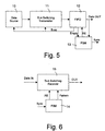
- Figures 5 and 6 illustrate the circuit architecture, at the transmission end and at the reception end, with which synchronization of the sorting pattern is obtained according to a first embodiment of the present invention.
- Figure 5 illustrates a data source 10, consisting for example of a digital processor, which supplies the data to be transmitted on the bus 2; a transmitter 11 having the function of encoding the data supplied by the data source 10 in the way previously described so as to reduce the bus switching activity; a FIFO (First In First Out) register 12 having the purpose of accumulating the data supplied by the transmitter 11 before their introduction onto the bus 2, for the reasons that will be clarified in what follows; and a finite state machine 13 having the purpose of generating the aforementioned synchronization signal through which the sorting pattern is transmitted.
- a data source 10 consisting for example of a digital processor
- transmitter 11 receives the data generated by the data source 10 and supplies said data encoded in the way described above, together with the corresponding sorting patterns, which are supplied to the FIFO register 12, which accumulates them progressively before their introduction onto the bus 2.
- Data accumulated in the FIFO register 12 are sent onto the bus 2 one at a time upon command of a read enable logic signal RE generated by the finite state machine 13 on the basis of the data and of the corresponding sorting patterns supplied thereto.
- the finite state machine 13 has a number of internal states equal to the number of possible sorting patterns, and each of its internal states is uniquely associated to a respective sorting pattern.
- the finite state machine 13 compares each sorting pattern that it receives from the transmitter 11 with its own internal state and, when these coincide, generates the aforementioned logic synchronization signal Sync, which is supplied to the receiver via a respective additional line of the bus, and through which the receiver recovers the sorting pattern used in transmission.
- the finite state machine 13 Upon detection of the coincidence between the sorting pattern to be transmitted and its own internal state, the finite state machine 13 generates the aforesaid read enable signal RE that controls the FIFO register 12 so as to extract from this a new datum and enter it on the bus.
- the FIFO register 12 generates a logic empty register signal Empty, indicating the fact that the FIFO register 12 does not contain data to be transmitted, and a logic transmission disabling signal Busy, indicating the fact that the FIFO register 12 is full and is hence no longer capable of accepting input data.
- the empty register signal Empty is supplied to the finite state machine 13 with the purpose of interrupting the generation of the synchronization signal Sync when the FIFO register 12 is empty, whilst the transmission disabling signal Busy is supplied both to the data source 10 and to the transmitter 11 for interrupting generation of new data to be transmitted and consequently interrupting supply of new data to the input of the FIFO register 12.
- Figure 6 illustrates a finite state machine 14 having the function of recovering the sorting pattern used in transmission, and a receiver 15 having the purpose of decoding the data transmitted using the recovered sorting pattern.
- the finite state machine 14 receives the synchronization signal Sync transmitted on the additional line of the bus and the empty register signal Empty and supplies the sorting pattern used in transmission and the read enable signal RE.
- the finite state machine 14 has a number of internal states equal to the number of possible sorting patterns, and each of its internal states is uniquely associated to a respective sorting pattern.
- the association between internal state and sorting pattern is exactly identical to that of the finite state machine 13.
- the finite state machine 14 is synchronized with the finite state machine 13, i.e., the internal states of the two finite state machines 13 and 14 coincide at each instant of time.
- the finite state machine 14 determines the sorting pattern associated to its internal state at that precise instant in time, a pattern that is exactly identical to the one transmitted.
- the synchronization between the two finite state machines is guaranteed by supplying to both the same clock signal CK.
- the receiver receives the data transmitted, the sorting pattern recovered, and the read enable signal RE, and supplies the data transmitted.
- the data transmitted are received, decoded using the sorting pattern recovered, and then supplied on the output of the receiver only after appropriate enabling provided by the read enable signal RE, which is generated locally by the finite state machine 14.
- the finite state machines 13 and 14 are designed so as to have a number of internal states equal to the number of possible sorting patterns, and the evolution from one state to the next occurs with a frequency that is determined as a function of the frequency with which the data are sent onto the bus, taking into account the considerations that emerge from what follows.
- the clock frequency at which the finite state machine 13 operates internally cannot be too high with respect to the one at which the data are introduced onto the bus in so far as such a high frequency is not physically available in the chip in which said architecture is made, and cannot be too low in so far as the time spent for transmitting the data would be unacceptably long.
- f FSM f bus ⁇ M
- f FSM represents the clock frequency of the finite state machine 13
- f bus represents the clock frequency of the bus
- M represents the number of attempts that are made in one bus cycle for identifying the sorting pattern
- the bus cycle being defined as the interval of time elapsing between two successive introductions of data on the bus
- the FIFO register 12 is physically unable to have an infinite storage capacity, so that it is necessary to take into account also the likelihood of inoperativeness. Consequently, when the FIFO register 12 is full, the transmission disabling signal Busy is generated, which interrupts precisely the transmission of the data.
- the technique according to the invention is particularly advantageous and presents good performance in the case where the transmission on the bus is of the burst type (for example AMBA BUS and PCI BUS) and the FIFO register is sized according to the width of the burst.
- the burst type for example AMBA BUS and PCI BUS
- the FIFO register 12 may conveniently be built using a process of birth and death of a Markov chain, which precisely makes it possible to determine a priori the probability of inoperativeness of the FIFO register 12 on the basis of the statistical information corresponding to the traffic.
- the finite state machines 13, 14 can go into the initial reset state either cyclically, after assuming all the possible internal states, or else after each recognition of a sorting pattern.
- the resetting of the finite state machines 13, 14, which can be achieved using precisely the synchronization signal Sync, which, as has been said, is complemented after each recognition of a sorting pattern, enables a further reduction in the transmission delay and is particularly advantageous in the case where the most probable sorting patterns, determined by a preventive analysis of the traffic, are associated to the first internal states of the finite state machines 13, 14.
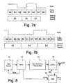
- Figures 7a and 7b show the synchronization signal Sync, the internal states of the finite state machines 13, 14 (considering finite state machines with four internal states S0, S1, S2 and S3), and the optimal sorting pattern transmitted when the finite state machines 13, 14 go into the initial reset state after assuming all the possible internal states ( Figure 7a) and, respectively, when the finite state machines 13, 14 go into the initial reset state after each recognition of a sorting pattern ( Figure 7b).
- Figure 8 illustrates a possible variant of the circuit architecture, at the transmission end, illustrated in Figure 5.
- the FIFO register 12 is arranged downstream of the transmitter 11 and stores temporarily both the data supplied by the transmitter 11 and the sorting patterns associated thereto
- the FIFO register 12 is arranged between the data source 10 and the transmitter 11 and stores the data supplied by the data source 10.
- the FIFO register 12 has a storage capacity considerably smaller than the one present in the embodiment of Figure 5, with consequent reduction in area occupied on the silicon.
- This variant requires however, that there be synchronization between the data and the sorting patterns transmitted by the transmitter and the generation of the synchronization signal Sync by the finite state machine 13 so as to enable a correct recognition of the data transmitted at the reception end.
- loading of the latch is enabled directly by the finite state machine 13 through the read enable signal RE that is generated by the latter when its internal state coincides with the sorting pattern to be transmitted, whilst in the other embodiment, not illustrated in Figure 8, the transmitter 11 is set in stand-by by the finite state machine 13 until the internal state of the latter coincides with the sorting pattern to be transmitted.
- the FIFO register 12 generates at output the empty register logic signal Empty for the finite state machine 13, which indicates the fact that the FIFO register 12 does not contain data to be transmitted, and the transmission disabling logic signal Busy for the data source 10, which indicates the fact that the FIFO register 12 is full and is thus no longer able to accept input data.
- Figures 9 and 10 illustrate the circuit architecture, at the transmission end and at the reception end, with which synchronization of the sorting pattern is obtained according to a second embodiment of the present invention, which is particularly advantageous when there are additional transmission lines on the bus that are freely usable.
- the second embodiment does not entail the use of a FIFO register in transmission, and its elimination is made possible by the adoption of a parallel architecture that exploits said additional free transmission lines in combination with the use of different sorting patterns.
- N / M finite state machines are used, in which N and M have the meanings indicated above, i.e., N is the number of possible sorting patterns and M is the number of times that the clock frequency of each finite state machine 13 is higher than the clock frequency of the bus.
- the finite state machines receive the sorting pattern supplied by the transmitter 11, and each of them supplies a corresponding synchronization signal, designated by Sync1, Sync2, Sync3 and Sync4, which is sent to the reception end through a corresponding additional line of the bus.
- the finite state machines have the same number of internal states smaller than the number N of possible sorting patterns, and associated to the internal states of each finite state machine is a subset of the possible sorting patterns that are distinct and disjoint with respect to the subsets associated to the other finite state machines; i.e., the subsets of the possible sorting patterns of the finite state machines do not contain elements in common.
- Each of the four finite state machines 13.1-13.4 has a number of internal states equal to four, and associated to the four internal states of each finite state machine are four of the possible sorting patterns. Furthermore, the four subsets of sorting patterns associated to the internal states of the four finite state machines 13.1-13.4 do not contain elements in common.
- each of the four finite state machines 13.1-13.4 compares the sorting pattern received with its own internal state, and given that the clock frequency of the finite state machines 13.1-13.4 is four times higher than the clock frequency of the bus, at the end of one bus cycle the sorting pattern to be transmitted will have been recognized, i.e., the internal state of one of the finite state machines 13.1-13.4 will certainly coincide with the sorting pattern to be transmitted.
- the finite state machine 13.1-13.4 Upon detection of the coincidence between the sorting pattern to be transmitted and its own internal state, the finite state machine 13.1-13.4 in question generates the corresponding synchronization signal Sync1-Sync4 that is sent to the reception end.
- the finite state machines 13.1-13.4 can go into the initial reset state, either cyclically after assuming all the possible internal states or else after each recognition of a sorting pattern.
- the synchronization signal Sync1-Sync4 generated by a finite state machine 13.1-13.4 is supplied also to all the other finite state machines 13.1-13.4, which are reset upon detection of the switching of any one of the synchronization signals Sync1-Sync4.
- N / M finite state machines each of which receives at input a corresponding synchronization signal Sync and supplies at output a corresponding sorting pattern and a corresponding read enable signal RE, and an arbiter which receives the sorting patterns and the read enable signals RE generated by the finite state machines and which supplies to the receiver the sorting pattern and the read enable signal RE generated by the finite state machine involved in the recognition of the sorting pattern.
- the finite state machines at the reception end are functionally identical to the finite state machines at the transmission end; i.e., they have the same number of internal states as the finite state machines at the transmission end, and associated to each one of them is the same subset of sorting patterns that is associated to the finite state machine at the transmission end, from which it receives the synchronization signal.
- the four finite state machines at the reception end are designated respectively by 14.1, 14.2, 14.3 and 14.4, the sorting patterns supplied by the latter are respectively designated by Pattern1, Pattern2, Pattern3 and Pattern4, the read enable signals generated by them are respectively designated by RE1, RE2, RE3 and RE4, and the arbiter is designated by 17.
- one of the four finite state machines 14.1-14.4 verifies that switching of the corresponding synchronization signal Sync1-Sync4 has occurred, it recovers the sorting pattern transmitted in the bus cycle in which said switching has occurred and generates the sorting pattern transmitted and the corresponding read enable signal, which, via the arbiter 17, are supplied to the receiver 15, which uses them for decoding the data transmitted.
- the finite state machines 14.1-14.4 can go into the initial reset state either cyclically after assuming all the possible internal states or else after each recognition of a sorting pattern. To ensure that all the finite state machines 14.1-14.4 go into the initial reset state after each recognition of a sorting pattern, each of the finite state machines 14.1-14.4 at the reception end receives all the synchronization signals generated by the finite state machines 13.1-13.4 at the transmission end so as to reset itself upon detection of switching of any one of the synchronization signals.
- each finite state machine 14.1-14.4 observes the following rules:
- the switching activity of the additional lines of the bus used for transmitting the synchronization signals is equal to the one that exists in the architecture according to the first embodiment of the present invention (illustrated in Figures 5 and 6) and in the corresponding variant (illustrated in Figure 8), in which just one finite state machine is used at the transmission end, and a corresponding finite state machine is used at the reception end in so far as in the second embodiment just one of the finite state machines at the transmission end recognizes the sorting pattern and generates the corresponding synchronization signal in each bus cycle.
- the inventive idea underlying the present invention is of altogether general application and can be used for transmitting data of any nature on a single line.
- n -bit datum it is sufficient to generate in succession all the possible combinations of n bits, compare the n -bit datum to be transmitted with the combinations of n bits generated, generate an identity signal upon detection of the coincidence between the n -bit datum to be transmitted and one of the combinations of n bits generated, and transmit the coincidence signal on the single line.
- the present invention is suitable for being implemented to particular advantage in the form of a computer product that can be loaded into a memory (typically a set of registers) of a processor associated to the bus and that comprises portions of software code which, when the computer product is run on the aforesaid processor, perform the steps of the methods according to the invention.
- a memory typically a set of registers
- the present invention is suitable for being implemented to particular advantage in the form of a computer product that can be loaded into a memory (typically a set of registers) of a processor associated to the bus and that comprises portions of software code which, when the computer product is run on the aforesaid processor, perform the steps of the methods according to the invention.
Landscapes
- Engineering & Computer Science (AREA)
- Theoretical Computer Science (AREA)
- Physics & Mathematics (AREA)
- General Engineering & Computer Science (AREA)
- General Physics & Mathematics (AREA)
- Information Transfer Systems (AREA)
- Communication Control (AREA)
Priority Applications (3)
| Application Number | Priority Date | Filing Date | Title |
|---|---|---|---|
| EP03425013A EP1439470B1 (de) | 2003-01-14 | 2003-01-14 | Verfahren und Gerät, um Daten über eine einzige Leitung zu übertragen, insbesondere um Busdaten mit Minimalisierung der Busschaltaktivität zu übertragen |
| DE60315122T DE60315122D1 (de) | 2003-01-14 | 2003-01-14 | Verfahren und Gerät, um Daten über eine einzige Leitung zu übertragen, insbesondere um Busdaten mit Minimalisierung der Busschaltaktivität zu übertragen |
| US10/757,772 US7586943B2 (en) | 2003-01-14 | 2004-01-14 | Method and device for transmitting data on a single line, in particular for transmitting data on a bus with minimization of the bus switching activity, and corresponding computer product |
Applications Claiming Priority (1)
| Application Number | Priority Date | Filing Date | Title |
|---|---|---|---|
| EP03425013A EP1439470B1 (de) | 2003-01-14 | 2003-01-14 | Verfahren und Gerät, um Daten über eine einzige Leitung zu übertragen, insbesondere um Busdaten mit Minimalisierung der Busschaltaktivität zu übertragen |
Publications (2)
| Publication Number | Publication Date |
|---|---|
| EP1439470A1 true EP1439470A1 (de) | 2004-07-21 |
| EP1439470B1 EP1439470B1 (de) | 2007-07-25 |
Family
ID=32524296
Family Applications (1)
| Application Number | Title | Priority Date | Filing Date |
|---|---|---|---|
| EP03425013A Expired - Lifetime EP1439470B1 (de) | 2003-01-14 | 2003-01-14 | Verfahren und Gerät, um Daten über eine einzige Leitung zu übertragen, insbesondere um Busdaten mit Minimalisierung der Busschaltaktivität zu übertragen |
Country Status (3)
| Country | Link |
|---|---|
| US (1) | US7586943B2 (de) |
| EP (1) | EP1439470B1 (de) |
| DE (1) | DE60315122D1 (de) |
Families Citing this family (3)
| Publication number | Priority date | Publication date | Assignee | Title |
|---|---|---|---|---|
| US8355400B2 (en) * | 2004-08-06 | 2013-01-15 | Lantiq Deutschland Gmbh | System and method for transmitting information over a plurality of communication links |
| US9116828B2 (en) | 2008-06-11 | 2015-08-25 | Micron Technology, Inc. | Data bus inversion usable in a memory system |
| WO2010002397A1 (en) | 2008-07-01 | 2010-01-07 | Hewlett-Packard Development Company, L.P. | Segmenting bus topology |
Citations (4)
| Publication number | Priority date | Publication date | Assignee | Title |
|---|---|---|---|---|
| US4667337A (en) * | 1985-08-28 | 1987-05-19 | Westinghouse Electric Corp. | Integrated circuit having outputs configured for reduced state changes |
| JPH0969075A (ja) * | 1995-08-31 | 1997-03-11 | Nippon Telegr & Teleph Corp <Ntt> | バス回路 |
| EP0886220A2 (de) * | 1997-06-02 | 1998-12-23 | Nokia Mobile Phones Ltd. | Speicherbusschnittstelle mit niedriger Leistung |
| US20020156953A1 (en) * | 2001-02-28 | 2002-10-24 | Beiley Mark A. | Dynamic bus inversion method |
Family Cites Families (9)
| Publication number | Priority date | Publication date | Assignee | Title |
|---|---|---|---|---|
| US4933897A (en) * | 1986-02-07 | 1990-06-12 | Advanced Micro Devices, Inc. | Method for designing a control sequencer |
| US5436928A (en) * | 1991-04-08 | 1995-07-25 | Nippon Telegraph And Telephone Corporation | Method and apparatus for equalizing transmission line characteristics which vary at high speed in mobile radio communication |
| US5586125A (en) * | 1993-02-26 | 1996-12-17 | Warner; William T. | Method for generating test vectors for characterizing and verifying the operation of integrated circuits |
| US5572736A (en) * | 1995-03-31 | 1996-11-05 | International Business Machines Corporation | Method and apparatus for reducing bus noise and power consumption |
| US5680300A (en) * | 1995-12-22 | 1997-10-21 | Analog Devices, Inc. | Regulated charge pump DC/DC converter |
| US5825644A (en) * | 1996-03-04 | 1998-10-20 | Motorola, Inc. | Method for encoding a state machine |
| US6813519B2 (en) * | 2000-01-21 | 2004-11-02 | Medtronic Minimed, Inc. | Ambulatory medical apparatus and method using a robust communication protocol |
| US7349005B2 (en) * | 2001-06-14 | 2008-03-25 | Microsoft Corporation | Automated video production system and method using expert video production rules for online publishing of lectures |
| DE60210438T2 (de) * | 2002-07-10 | 2006-10-12 | Stmicroelectronics S.R.L., Agrate Brianza | Verfahren und Gerät zur Verminderung der Busschaltaktivität und Rechnerprogrammprodukt |
-
2003
- 2003-01-14 DE DE60315122T patent/DE60315122D1/de not_active Expired - Lifetime
- 2003-01-14 EP EP03425013A patent/EP1439470B1/de not_active Expired - Lifetime
-
2004
- 2004-01-14 US US10/757,772 patent/US7586943B2/en active Active
Patent Citations (4)
| Publication number | Priority date | Publication date | Assignee | Title |
|---|---|---|---|---|
| US4667337A (en) * | 1985-08-28 | 1987-05-19 | Westinghouse Electric Corp. | Integrated circuit having outputs configured for reduced state changes |
| JPH0969075A (ja) * | 1995-08-31 | 1997-03-11 | Nippon Telegr & Teleph Corp <Ntt> | バス回路 |
| EP0886220A2 (de) * | 1997-06-02 | 1998-12-23 | Nokia Mobile Phones Ltd. | Speicherbusschnittstelle mit niedriger Leistung |
| US20020156953A1 (en) * | 2001-02-28 | 2002-10-24 | Beiley Mark A. | Dynamic bus inversion method |
Non-Patent Citations (1)
| Title |
|---|
| PATENT ABSTRACTS OF JAPAN vol. 1997, no. 07 31 July 1997 (1997-07-31) * |
Also Published As
| Publication number | Publication date |
|---|---|
| DE60315122D1 (de) | 2007-09-06 |
| EP1439470B1 (de) | 2007-07-25 |
| US7586943B2 (en) | 2009-09-08 |
| US20040218629A1 (en) | 2004-11-04 |
Similar Documents
| Publication | Publication Date | Title |
|---|---|---|
| US6594275B1 (en) | Fibre channel host bus adapter having multi-frequency clock buffer for reduced power consumption | |
| JP2002007201A (ja) | メモリシステム、メモリインターフェース及びメモリチップ | |
| US6741193B2 (en) | Parallel in serial out circuit having flip-flop latching at multiple clock rates | |
| US6999352B2 (en) | Data inversion circuit and semiconductor device | |
| US6393082B1 (en) | Signal synchronism detecting circuit | |
| CN112394281A (zh) | 测试信号并行加载转换电路和系统级芯片 | |
| US8023602B2 (en) | Serial data communication apparatus and methods of using a single line | |
| US7924185B2 (en) | Semiconductor integrated circuit device, pattern detection method and serial-parallel conversion method | |
| US20180241539A1 (en) | Semiconductor device and data synchronization method | |
| EP1439470B1 (de) | Verfahren und Gerät, um Daten über eine einzige Leitung zu übertragen, insbesondere um Busdaten mit Minimalisierung der Busschaltaktivität zu übertragen | |
| EP3734465A1 (de) | Datenübertragungscode und -schnittstelle | |
| CN103107862A (zh) | 逻辑器件及其mdio数据发送方法 | |
| JP3434149B2 (ja) | フレーム同期信号検出装置 | |
| US5331668A (en) | Communication control device | |
| US6920578B1 (en) | Method and apparatus for transferring data between a slower clock domain and a faster clock domain in which one of the clock domains is bandwidth limited | |
| EP2006777A1 (de) | Verfahren und Vorrichtung zur Erzeugung von invertiertem Code auf einem Bus | |
| US6633613B1 (en) | Digital circuit for formatting and compressing radar video data | |
| CN113364468A (zh) | 串并转换对齐电路及方法 | |
| EP0282924B1 (de) | Kodierschaltung mit bipolarer Acht- und Sechsnullfolgensubstitution | |
| JPH0654121A (ja) | 高密度熱記録ヘッドのためのデータ伝達装置 | |
| JPH05250316A (ja) | 装置間インタフェース方式 | |
| JPH0738605A (ja) | デジタルデ−タパケットスイッチングモジュール | |
| US12301233B2 (en) | Ultra low latency pattern matching system and method | |
| JP3052848B2 (ja) | フレーム同期保護回路 | |
| KR100677199B1 (ko) | 인터럽트 처리장치 |
Legal Events
| Date | Code | Title | Description |
|---|---|---|---|
| PUAI | Public reference made under article 153(3) epc to a published international application that has entered the european phase |
Free format text: ORIGINAL CODE: 0009012 |
|
| AK | Designated contracting states |
Kind code of ref document: A1 Designated state(s): AT BE BG CH CY CZ DE DK EE ES FI FR GB GR HU IE IT LI LU MC NL PT SE SI SK TR |
|
| AX | Request for extension of the european patent |
Extension state: AL LT LV MK RO |
|
| RTI1 | Title (correction) |
Free format text: METHOD AND DEVICE FOR TRANSMITTING DATA ON A SINGLE LINE, IN PARTICULAR FOR TRANSMITTING DATA ON A BUS WITH MINIMIZATION |
|
| 17P | Request for examination filed |
Effective date: 20050119 |
|
| AKX | Designation fees paid |
Designated state(s): DE FR GB IT |
|
| GRAP | Despatch of communication of intention to grant a patent |
Free format text: ORIGINAL CODE: EPIDOSNIGR1 |
|
| GRAS | Grant fee paid |
Free format text: ORIGINAL CODE: EPIDOSNIGR3 |
|
| GRAA | (expected) grant |
Free format text: ORIGINAL CODE: 0009210 |
|
| AK | Designated contracting states |
Kind code of ref document: B1 Designated state(s): DE FR GB IT |
|
| REG | Reference to a national code |
Ref country code: GB Ref legal event code: FG4D |
|
| RIN1 | Information on inventor provided before grant (corrected) |
Inventor name: VISALLI, GIUSEPPE Inventor name: PAPPALARDO, FRANCESCO |
|
| REF | Corresponds to: |
Ref document number: 60315122 Country of ref document: DE Date of ref document: 20070906 Kind code of ref document: P |
|
| ET | Fr: translation filed | ||
| PLBE | No opposition filed within time limit |
Free format text: ORIGINAL CODE: 0009261 |
|
| STAA | Information on the status of an ep patent application or granted ep patent |
Free format text: STATUS: NO OPPOSITION FILED WITHIN TIME LIMIT |
|
| 26N | No opposition filed |
Effective date: 20080428 |
|
| PG25 | Lapsed in a contracting state [announced via postgrant information from national office to epo] |
Ref country code: DE Free format text: LAPSE BECAUSE OF FAILURE TO SUBMIT A TRANSLATION OF THE DESCRIPTION OR TO PAY THE FEE WITHIN THE PRESCRIBED TIME-LIMIT Effective date: 20071026 |
|
| PGFP | Annual fee paid to national office [announced via postgrant information from national office to epo] |
Ref country code: FR Payment date: 20080131 Year of fee payment: 6 |
|
| REG | Reference to a national code |
Ref country code: FR Ref legal event code: ST Effective date: 20091030 |
|
| PG25 | Lapsed in a contracting state [announced via postgrant information from national office to epo] |
Ref country code: FR Free format text: LAPSE BECAUSE OF NON-PAYMENT OF DUE FEES Effective date: 20090202 |
|
| PGFP | Annual fee paid to national office [announced via postgrant information from national office to epo] |
Ref country code: GB Payment date: 20131223 Year of fee payment: 12 |
|
| PGFP | Annual fee paid to national office [announced via postgrant information from national office to epo] |
Ref country code: IT Payment date: 20131220 Year of fee payment: 12 |
|
| GBPC | Gb: european patent ceased through non-payment of renewal fee |
Effective date: 20150114 |
|
| PG25 | Lapsed in a contracting state [announced via postgrant information from national office to epo] |
Ref country code: GB Free format text: LAPSE BECAUSE OF NON-PAYMENT OF DUE FEES Effective date: 20150114 |
|
| PG25 | Lapsed in a contracting state [announced via postgrant information from national office to epo] |
Ref country code: IT Free format text: LAPSE BECAUSE OF NON-PAYMENT OF DUE FEES Effective date: 20150114 |