EP1439582A2 - Bildsensor mit Kupfer-Leiterbahnen und Herstellungsverfahren dafür - Google Patents
Bildsensor mit Kupfer-Leiterbahnen und Herstellungsverfahren dafür Download PDFInfo
- Publication number
- EP1439582A2 EP1439582A2 EP03018706A EP03018706A EP1439582A2 EP 1439582 A2 EP1439582 A2 EP 1439582A2 EP 03018706 A EP03018706 A EP 03018706A EP 03018706 A EP03018706 A EP 03018706A EP 1439582 A2 EP1439582 A2 EP 1439582A2
- Authority
- EP
- European Patent Office
- Prior art keywords
- layer
- interlayer dielectric
- forming
- copper
- photodiode
- Prior art date
- Legal status (The legal status is an assumption and is not a legal conclusion. Google has not performed a legal analysis and makes no representation as to the accuracy of the status listed.)
- Granted
Links
Images














Classifications
-
- H—ELECTRICITY
- H10—SEMICONDUCTOR DEVICES; ELECTRIC SOLID-STATE DEVICES NOT OTHERWISE PROVIDED FOR
- H10F—INORGANIC SEMICONDUCTOR DEVICES SENSITIVE TO INFRARED RADIATION, LIGHT, ELECTROMAGNETIC RADIATION OF SHORTER WAVELENGTH OR CORPUSCULAR RADIATION
- H10F77/00—Constructional details of devices covered by this subclass
- H10F77/20—Electrodes
- H10F77/206—Electrodes for devices having potential barriers
-
- H—ELECTRICITY
- H10—SEMICONDUCTOR DEVICES; ELECTRIC SOLID-STATE DEVICES NOT OTHERWISE PROVIDED FOR
- H10F—INORGANIC SEMICONDUCTOR DEVICES SENSITIVE TO INFRARED RADIATION, LIGHT, ELECTROMAGNETIC RADIATION OF SHORTER WAVELENGTH OR CORPUSCULAR RADIATION
- H10F39/00—Integrated devices, or assemblies of multiple devices, comprising at least one element covered by group H10F30/00, e.g. radiation detectors comprising photodiode arrays
- H10F39/011—Manufacture or treatment of image sensors covered by group H10F39/12
- H10F39/024—Manufacture or treatment of image sensors covered by group H10F39/12 of coatings or optical elements
-
- H—ELECTRICITY
- H10—SEMICONDUCTOR DEVICES; ELECTRIC SOLID-STATE DEVICES NOT OTHERWISE PROVIDED FOR
- H10F—INORGANIC SEMICONDUCTOR DEVICES SENSITIVE TO INFRARED RADIATION, LIGHT, ELECTROMAGNETIC RADIATION OF SHORTER WAVELENGTH OR CORPUSCULAR RADIATION
- H10F39/00—Integrated devices, or assemblies of multiple devices, comprising at least one element covered by group H10F30/00, e.g. radiation detectors comprising photodiode arrays
- H10F39/011—Manufacture or treatment of image sensors covered by group H10F39/12
- H10F39/026—Wafer-level processing
-
- H—ELECTRICITY
- H10—SEMICONDUCTOR DEVICES; ELECTRIC SOLID-STATE DEVICES NOT OTHERWISE PROVIDED FOR
- H10F—INORGANIC SEMICONDUCTOR DEVICES SENSITIVE TO INFRARED RADIATION, LIGHT, ELECTROMAGNETIC RADIATION OF SHORTER WAVELENGTH OR CORPUSCULAR RADIATION
- H10F39/00—Integrated devices, or assemblies of multiple devices, comprising at least one element covered by group H10F30/00, e.g. radiation detectors comprising photodiode arrays
- H10F39/80—Constructional details of image sensors
- H10F39/805—Coatings
- H10F39/8057—Optical shielding
-
- H—ELECTRICITY
- H10—SEMICONDUCTOR DEVICES; ELECTRIC SOLID-STATE DEVICES NOT OTHERWISE PROVIDED FOR
- H10F—INORGANIC SEMICONDUCTOR DEVICES SENSITIVE TO INFRARED RADIATION, LIGHT, ELECTROMAGNETIC RADIATION OF SHORTER WAVELENGTH OR CORPUSCULAR RADIATION
- H10F39/00—Integrated devices, or assemblies of multiple devices, comprising at least one element covered by group H10F30/00, e.g. radiation detectors comprising photodiode arrays
- H10F39/80—Constructional details of image sensors
- H10F39/806—Optical elements or arrangements associated with the image sensors
-
- H—ELECTRICITY
- H10—SEMICONDUCTOR DEVICES; ELECTRIC SOLID-STATE DEVICES NOT OTHERWISE PROVIDED FOR
- H10F—INORGANIC SEMICONDUCTOR DEVICES SENSITIVE TO INFRARED RADIATION, LIGHT, ELECTROMAGNETIC RADIATION OF SHORTER WAVELENGTH OR CORPUSCULAR RADIATION
- H10F39/00—Integrated devices, or assemblies of multiple devices, comprising at least one element covered by group H10F30/00, e.g. radiation detectors comprising photodiode arrays
- H10F39/80—Constructional details of image sensors
- H10F39/806—Optical elements or arrangements associated with the image sensors
- H10F39/8063—Microlenses
-
- H—ELECTRICITY
- H10—SEMICONDUCTOR DEVICES; ELECTRIC SOLID-STATE DEVICES NOT OTHERWISE PROVIDED FOR
- H10F—INORGANIC SEMICONDUCTOR DEVICES SENSITIVE TO INFRARED RADIATION, LIGHT, ELECTROMAGNETIC RADIATION OF SHORTER WAVELENGTH OR CORPUSCULAR RADIATION
- H10F39/00—Integrated devices, or assemblies of multiple devices, comprising at least one element covered by group H10F30/00, e.g. radiation detectors comprising photodiode arrays
- H10F39/80—Constructional details of image sensors
- H10F39/806—Optical elements or arrangements associated with the image sensors
- H10F39/8067—Reflectors
-
- H—ELECTRICITY
- H10—SEMICONDUCTOR DEVICES; ELECTRIC SOLID-STATE DEVICES NOT OTHERWISE PROVIDED FOR
- H10F—INORGANIC SEMICONDUCTOR DEVICES SENSITIVE TO INFRARED RADIATION, LIGHT, ELECTROMAGNETIC RADIATION OF SHORTER WAVELENGTH OR CORPUSCULAR RADIATION
- H10F39/00—Integrated devices, or assemblies of multiple devices, comprising at least one element covered by group H10F30/00, e.g. radiation detectors comprising photodiode arrays
- H10F39/80—Constructional details of image sensors
- H10F39/811—Interconnections
-
- H—ELECTRICITY
- H10—SEMICONDUCTOR DEVICES; ELECTRIC SOLID-STATE DEVICES NOT OTHERWISE PROVIDED FOR
- H10W—GENERIC PACKAGES, INTERCONNECTIONS, CONNECTORS OR OTHER CONSTRUCTIONAL DETAILS OF DEVICES COVERED BY CLASS H10
- H10W20/00—Interconnections in chips, wafers or substrates
- H10W20/40—Interconnections external to wafers or substrates, e.g. back-end-of-line [BEOL] metallisations or vias connecting to gate electrodes
- H10W20/41—Interconnections external to wafers or substrates, e.g. back-end-of-line [BEOL] metallisations or vias connecting to gate electrodes characterised by their conductive parts
- H10W20/425—Barrier, adhesion or liner layers
-
- H—ELECTRICITY
- H10—SEMICONDUCTOR DEVICES; ELECTRIC SOLID-STATE DEVICES NOT OTHERWISE PROVIDED FOR
- H10W—GENERIC PACKAGES, INTERCONNECTIONS, CONNECTORS OR OTHER CONSTRUCTIONAL DETAILS OF DEVICES COVERED BY CLASS H10
- H10W20/00—Interconnections in chips, wafers or substrates
- H10W20/01—Manufacture or treatment
- H10W20/031—Manufacture or treatment of conductive parts of the interconnections
- H10W20/032—Manufacture or treatment of conductive parts of the interconnections of conductive barrier, adhesion or liner layers
- H10W20/054—Manufacture or treatment of conductive parts of the interconnections of conductive barrier, adhesion or liner layers by selectively removing parts thereof
Definitions
- the present invention relates to a structure of a photodiode image sensor device and a method for fabricating the same. More particularly, the present invention relates to a photodiode image sensor device having a copper interconnection and a method for fabricating the same.
- a photodiode image sensor converts optical information into electrical signals.
- solid state image sensor devices There are basically two different types of solid state image sensor devices: a MOS (metal-oxide-semiconductor) type and a CCD (charge coupled device) type.
- Products employing photodiodes include those that employ contact image sensors (CISs) such as hand held phones (HHPs), cameras including those integrated into cellular phones, and scanners.
- CISs contact image sensors
- HHPs hand held phones
- CCDs charge coupled devices
- CCTV cameras camcorders and digital cameras.
- Copper has been suggested as an alternative to aluminum in applications where the design rule or pattern thickness is below 0.13 ⁇ m.
- copper atoms tend to diffuse into surrounding materials, such as into an interlayer dielectric layer, and can negatively impact the electrical characteristics of underlying transistors or other elements. Therefore, in order to use copper as an interconnection material in an integrated circuit device, a diffusion barrier layer is necessary to prevent diffusion of the copper into surrounding materials.
- a diffusion barrier layer is formed of SiN or SiC.
- these materials are opaque, and therefore negatively impact the performance of image devices having a photodiode, which depends completely on the level of external light that it receives.
- the invention solves this problem by providing an image sensor device according to claim 1 or 2 and a method according to claim 16. Further advantageous embodiments of the invention are mentioned in the subclaims, the wording of which is herewith fully incorporated into the description by reference to avoid unnecessary text repetitions.
- an image sensor device including a substrate having a photodiode formed therein, an isolation region formed in the substrate to a first side of the photodiode, and a plurality of transistors formed on the substrate to a second side of the photodiode, the photodiode being electrically associated with the transistors, at least one lower contact formed on source/drain regions and gates of the transistors, at least one electrical interconnection line formed on the at least one lower contact and being electrically associated with the photodiode, a light passageway having a light inlet, the light passageway being positioned in alignment with the photodiode, a color filter positioned over the light inlet of the light passageway; and a lens positioned over the color filter in alignment with the light passageway, wherein the at least one electrical interconnection line includes a copper interconnection formation running through a plurality of interlayer dielectric layers in a stacked configuration with a diffusion barrier layer between adjacent interlayer dielectric layers, and a barrier metal
- the photodiode may be a p/n photodiode, a PIN photodiode, or an avalanche photodiode.
- the image sensor device may be a charge coupled device or a contact image sensor.
- the image sensor device may further include a first protection layer covering the uppermost surface of the copper interconnection, which may be formed of one selected from the group consisting of SiC, SiN, SiO 2 on SiN, and SiO 2 on SiC.
- the image sensor device may further include a second protection layer disposed on the first protection layer and an inner surface of the light passageway, which may be formed of a silicon oxide series material.
- the second protection layer may have an antireflective property at a bottom of the light passageway.
- the lower contact may be formed of one selected from the group consisting of copper, tungsten and titanium.
- a barrier metal layer to prevent copper diffusion may be interposed between the lower contact and the first of the plurality of interlayer dielectric layers.
- the image sensor may further include an antireflective layer formed on the substrate having the photodiode, the plurality of transistors and the isolation region, or the image sensor device may include an antireflective layer patterned on the photodiode under the light passageway.
- the light passageway may be filled with a transparent material such as a spin-on-glass (SOG) or a photoresist.
- the color filter may include a photoresist containing dies.
- the lens may be a convexly shaped micro lens.
- the image sensor device may further include a barrier metal layer on sidewalls of the light passageway.
- It is another aspect of the present invention to provide a method for forming an image sensor device including forming a photodiode in a substrate, forming an isolation region in the substrate to a first side of the photodiode, forming a plurality of transistors on the substrate to a second side of the photodiode, the transistors having source/drain regions and a gate, forming on the substrate having the photodiode an interlayer dielectric structure having a plurality of alternately stacked interlayer dielectric layers and diffusion barrier layers with an uppermost layer being an interlayer dielectric layer, and concurrently forming at least one electrical connection line formed of a copper interconnection within a barrier metal layer through the alternately stacked interlayer dielectric layers and diffusion barrier layers to be electrically associated with the photodiode and the at least one transistor, forming a light passageway having a light inlet in alignment with the photodiode by removing portions of the interlayer dielectric structure over the photodiode, forming a color filter over the light in
- the photodiode may be formed to be one selected from the group consisting of a p/n photodiode, a PIN photodiode and an avalanche photodiode.
- forming the interlayer dielectric structure and the light passageway further includes, A. forming a first interlayer dielectric layer of a transparent material on the substrate having the photodiode, the isolation region and the plurality of transistors, B. patterning the first interlayer dielectric layer to form contact holes over source/drain regions and gates of the transistors, C. filling the contact holes with metal to form lower contacts D. sequentially forming a first diffusion barrier layer and a second interlayer dielectric layer on the first interlayer dielectric layer, E. patterning the second interlayer dielectric layer and the first diffusion barrier layer to form via holes over the lower contacts, F. patterning the second interlayer dielectric layer to form trenches over the via holes, G.
- H. filling the via holes and the trenches with copper to form a copper interconnection
- J. forming a first protective layer on the copper interconnection in the uppermost interlayer dielectric layer before forming the light passageway
- K. filling the light passageway with a transparent material before forming the color filter and the lens.
- forming the light passageway includes sequentially etching a portion of each interlayer dielectric layer and diffusion barrier layer at a position over the photodiode down to the first interlayer dielectric layer.
- the method further includes patterning the second interlayer dielectric layer and the first diffusion barrier layer to also form a dummy hole over the photodiode in E, forming the barrier metal layer in the dummy hole in G, and filling the dummy hole with copper to form a copper dummy pattern in addition to the copper interconnection in H.
- Forming the light passageway preferably includes performing a wet etching process to remove the copper dummy patterns positioned over the photodiode and removing the barrier metal layer remaining on a bottom and sidewalls of the light passageway.
- the method further includes patterning the second interlayer dielectric layer and the first diffusion barrier layer to also form two dummy holes over opposite ends of the photodiode in E, thereby forming an interlayer dielectric dummy pattern over the photodiode in between the two dummy holes, forming the barrier metal layer in the dummy holes in G, and filling the dummy holes with copper in H.
- the widths of the two dummy holes and the via holes are preferably the same.
- the interlayer dielectric dummy pattern may be etched while the trenches are etched in F, such that the interlayer dielectric dummy pattern has a height equal to a depth of the trenches.
- Forming the light passageway preferably includes performing a wet etching process on the copper in the dummy holes, thereby removing the copper in the dummy holes and the interlayer dielectric dummy patterns.
- Forming the interconnections in H preferably includes forming a copper layer on the interlayer dielectric layer to fill the via holes and trenches, and planarizing the copper layer by chemical mechanical polishing to expose a surface of the underlying interlayer dielectric layer.
- the method further includes forming a barrier metal layer in the contact holes before filling the contact holes with the metal.
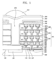
- FIG. 1 illustrates a cross-sectional view of a photodiode image sensor device according to a first embodiment of the present invention
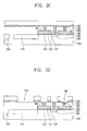
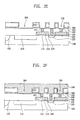
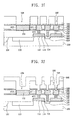
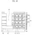
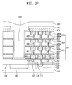
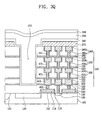
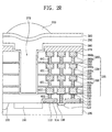
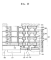
- FIGS. 2A-2R illustrate cross-sectional views of the photodiode image sensor device illustrated in FIG. 1 at various stages of formation for showing a method for forming an image sensor device according to a first embodiment of the present invention
- FIG. 3 illustrates a cross-sectional view of a photodiode image sensor device according to another embodiment of the present invention
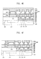
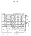
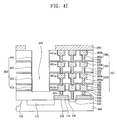
- FIGS. 4A-4J illustrate cross-sectional views of the photodiode image sensor device illustrated in FIG. 3 at various stages of formation for showing a method for forming an image sensor device according to a second embodiment of the present invention
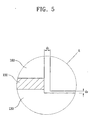
- FIG. 5 illustrates an enlarged view of section "A" of FIG. 4A.
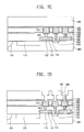
- FIGS. 6A-6H illustrate cross-sectional views of the photodiode image sensor device illustrated in FIG. 3 at various stages of formation for showing an alternate method for forming an image sensor device according to a third embodiment of the present invention
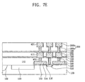
- FIGS. 7A-7H illustrate cross-sectional views of the photodiode image sensor device illustrated in FIG. 1 at various stages of formation for showing an alternate method for forming an image sensor device according to a fourth embodiment of the present invention
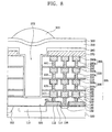
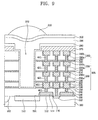
- FIGS. 8 and 9 illustrate cross-sectional views of a photodiode image sensor device having an antireflection layer according to the present invention.
- an image sensor device is provided as illustrated in FIG. 1.
- the image sensor device includes a substrate 100 having a p/n photodiode 110, which is a light-receiving element, formed therein, an isolation region 102 formed in the substrate 100 to a first side of the p/n photodiode 110, and a plurality of transistors 120 formed on the substrate 100 to a second side of the p/n photodiode 110.
- Each of the plurality of transistors 120 includes a gate insulating layer 112, a gate electrode 114, a source/drain region 122 and spacers 116.
- An electrical interconnection line 105 contacts source/drain region 122 and gate electrode 114 of transistors 120 by contacts 140.
- a transistor 120 is connected with the p/n photodiode 110, and receives electrons generated by the p/n photodiode 110 when light incident on the p/n diode has sufficient energy to generate electron-hole pairs.
- Light is transmitted to the p/n photodiode 110 through a light passageway 272 positioned in alignment with the p/n photodiode 110.
- the energetic, light-induced charges move to create a current that flows through the electrical interconnection line 105, which is in electrical connection with the p/n photodiode 110 via the transistors 120.
- the p/n photodiode 110 of the image sensor device converts light energy to electric energy by the process just described.
- the image sensor device further includes a color filter 300 formed over the light passageway 272 and a lens 310 formed on the color filter 300.
- the electrical interconnection line comprises copper interconnections 170, 200, 230, and 260 formed respectively in barrier metal layers 411, 421, 431 and 441, to prevent diffusion of copper atoms into interlayer dielectric layers 130, 160, 190, 220, and 250, where they can travel to the transistors 120 and cause adverse electrical effects.
- Copper interconnections 200, 230, and 260 are respectively formed of trenches 200b, 230b, and 260b, and vias 200a, 230a, and 260b.
- Diffusion barrier layers 150, 180, 210, and 240 are formed between adjacent interlayer dielectric layers.
- the image sensor device further includes a first protection layer 270 formed on the uppermost copper interconnection 260 in the uppermost interlayer dielectric layer 250, where it serves to protect the electrical interconnection line 105 when the light passageway 272 is formed over the p/n photodiode 110.
- a first protection layer 270 formed on the uppermost copper interconnection 260 in the uppermost interlayer dielectric layer 250, where it serves to protect the electrical interconnection line 105 when the light passageway 272 is formed over the p/n photodiode 110.
- FIG. 1 illustrates a second protection layer 280, which may be formed on the first protection layer 270 and on an inner surface of the light passageway 272.
- the present invention provides methods by which copper interconnections may be used in an image sensor device, thereby allowing fabrication of an image sensor device having a design rule or pattern thickness of less than 0.13 ⁇ m.
- the image sensor device may further include an antireflection layer 500 formed on the substrate, as illustrated in FIG. 8.
- the image sensor device may include an antireflection layer pattern 501 under the light passageway 272, as illustrated in FIG. 9.
- a portion of the second protection layer at a bottom of the light passageway 272 may be formed of an antireflective material, in which case an additional antireflection layer such as 500 or 501 is not necessary.
- a p/n photodiode 110 which is a light receiving element, is formed in a semiconductor substrate 100, an isolation region 102 is formed to a first side of the p/n photodiode 110, and a plurality of transistors 120 are formed to a second side of the p/n photodiode 110.
- Each transistor 120 includes a gate insulating layer 112, a gate electrode 114, a source/drain region 122 and spacers 116.
- a first interlayer dielectric layer 130 is formed of a transparent material such as a silicon oxide.
- the first interlayer dielectric layer 130 is patterned using known techniques, such as depositing and developing a photoresist material to make a mask pattern, through which dielectric material may be removed.
- a pattern of the dielectric material is removed by an etch process such as plasma etching or reactive ion etching, to form contact holes 132, which expose portions of the source/drain regions 122 and the gate electrodes 114.
- a first barrier metal layer 400 may be formed on the first interlayer dielectric layer 130 and in the contact holes 132.
- the contact holes 132 are then filled with a metal 138 such as titanium, tungsten or copper.
- the metal 138 may be deposited by electroplating, electroless plating, chemical vapor deposition, physical vapor deposition or any combination thereof.
- a barrier metal layer 400 in the contact holes for preventing copper diffusion.
- the first barrier metal layer 400 may be formed using a standard sputtering method.
- excess metal 138 (of FIG. 2B) and first barrier metal layer 400 (of FIG. 2B) may be removed by a method such as chemical mechanical polishing to expose the surface of the first interlayer dielectric layer 130, thereby forming lower contacts 140 on portions of the first barrier metal layer 401 in the contact holes 132 (of FIG. 2A).
- a first diffusion barrier layer 150 and a second interlayer dielectric layer 160 are sequentially formed on the first interlayer dielectric layer 130.
- the diffusion barrier layer 150 acts to prevent copper from diffusing into the interlayer dielectric layer 130, thereby protecting the underlying transistors 120 which are sensitive to copper diffusion.
- the diffusion barrier layer 150 further acts as an etch stop layer.
- the diffusion barrier layer 150 may be formed of SiN or SiC, but SiC may further include N or O and SiN may further include O.
- the thickness of the diffusion barrier layer 150 may be 200 ⁇ 1000 ⁇ , and is preferably 300 ⁇ 700 ⁇ . Because SiN and SiC are opaque, portions of the barrier layer must be removed to prevent filtering of light before the light reaches the p/n photodiode 110.
- First dummy hole 164 and first trenches 162 are then etched in the second interlayer dielectric layer 160 and the first diffusion barrier layer 150, to be over the p/n photodiode 110 and the lower contacts 140, respectively, as shown in FIG. 2D.
- First trenches 162 and first dummy hole 164 are formed using known damascene techniques.
- a width of the bottom of the dummy hole 164 is made to be slightly smaller than a width of the photodiode 110.
- a second barrier metal layer 410 is formed on the second interlayer dielectric layer 160 and in the trenches 162 and dummy hole 164, as shown in FIG. 2E.
- a first copper layer 159 is formed on the second barrier metal layer 410.
- the first copper layer 159 may be formed by first depositing a copper seed layer by sputtering, and then electroplating. Other methods, such as electroless plating, chemical vapor deposition, physical vapor deposition or a combination thereof may also be used to form the first copper layer 159.
- the first copper layer 159 is planarized by, for example, CMP to form first copper dummy pattern 172 and lower interconnections 170 in the first dummy hole 164 and first trenches 162, respectively, as shown in FIG. 2G.
- Second barrier metal layer 410 is also removed to expose an upper surface of the second interlayer dielectric layer 160, and to leave portions of the second barrier metal layer 413 and 411 in the first dummy holes 164 and the first trenches 162, respectively, to prevent diffusion of copper atoms into the surrounding interlayer dielectric layers.
- a second diffusion barrier layer 180 is then formed on the second interlayer dielectric layer 160, and a third interlayer dielectric layer 190 is formed on the second diffusion barrier layer 180.
- the height of the third interlayer dielectric layer 190 is preferably between 2,000 and 20,000 ⁇ .
- the third interlayer dielectric layer 190 is patterned using known techniques, such as the use of a photoresist material to expose and define a via pattern. After development, the photoresist acts as a mask through which the dielectric material via pattern is removed, thereby forming pre-via holes 192. At the same time, a pre-dummy hole 194 is formed in the third interlayer dielectric layer 190 over the first copper dummy pattern 172.
- the second diffusion barrier layer 180 remains in the bottom of the second pre-via holes 192 and the second pre-dummy hole 194. This is because the etch selectivity of the third interlayer dielectric layer 190 is higher than that of the second diffusion barrier 180.
- the third interlayer dielectric layer 190 is again patterned using known techniques to form a second trench 196. If a photoresist is used, then after development, the photoresist acts as a mask through which the dielectric material of the trench pattern is removed. Preferably, the height of the trench 196 is 2,000 ⁇ 10,000 ⁇ .
- the second diffusion barrier layer 180 is removed from bottoms of the pre-via holes 192 and pre-dummy hole 194 to thereby form second via holes 198 and second dummy hole 195.
- the pre-via hole 192 is formed first, and then a trench 196 and via holes 198 are formed.
- the trench may be formed first.
- a single damascene method may be used to form the via holes 198 and the trench 196.
- a third barrier metal layer 420 is then formed on the assembly by, for example, sputtering.
- a second copper layer 199 is then deposited on the assembly and in the dummy holes 195, via holes 198 and trenches 196.
- the second copper layer 199 is polished by, for example, CMP in a manner similar to that for the first copper layer 159 (as seen in FIG. 2G).
- portions of the third barrier metal layer 420 are removed to expose an upper surface of the third interlayer dielectric layer 190.
- a second copper dummy pattern 202 and a first interconnection 200, made up of trenches 200b and vias 200a, are thereby formed on portions of the third barrier metal layer 423 and 421, respectively, as shown in FIG. 2J.
- a third diffusion barrier layer 210 and a fourth interlayer dielectric layer 220 are sequentially formed on the third interlayer dielectric layer 190, and are patterned in a same manner as with the second diffusion barrier layer 180 and the third interlayer dielectric layer 190 as described above to form via holes, trenches and dummy holes (not shown).
- a fourth barrier metal layer (not shown) and a third copper layer (not shown) are then formed on the fourth interlayer dielectric layer 220 to fill the via holes, trenches and dummy holes. Forming the via holes, trenches and dummy holes is carried out in a same manner as with the third barrier metal layer 420 and second copper layer 199 as described above.
- the third copper layer is polished by, for example, CMP, and portions of the fourth barrier metal layer are removed to expose an upper surface of the fourth interlayer dielectric layer 220, thereby forming third copper dummy pattern 232 and second interconnection 230, made up of trenches 230b and vias 230a, on portions of the fourth barrier metal layer 433 and 431, respectively.
- the process is repeated using a fourth diffusion barrier layer 240 and a fifth interlayer dielectric layer 250, which are patterned to form via holes, trenches and dummy holes (not shown). Then a fifth barrier metal layer (not shown) and a fourth copper layer (not shown) are formed on the fifth interlayer dielectric layer 250 to fill the via holes, trenches and dummy holes.
- the fourth copper layer is then polished by, for example, CMP and portions of the fifth barrier metal layer are removed to expose an upper surface of the fifth interlayer dielectric layer 250, thereby forming fourth copper dummy pattern 262 and third interconnection 260, made up of trenches 260b and vias 260a, on portions of the fifth barrier metal layer 443 and 441, respectively, as shown in FIG. 2N.
- a first protection layer 270 is formed on a surface of the copper interconnection in the uppermost interlayer dielectric layer, in this case, the third interconnection 260 and the fifth interlayer dielectric layer 250.
- the first protection layer 270 is patterned using known techniques such as with the use of a photoresist material.
- the first protection layer 270 may be formed of SiN or SiC. However, deposition rates of SiN and SiC are slow, and if SiN or SiC is deposited too thickly, cracks may occur due to stress. Therefore, SiO 2 on SiN or SiC may also be used, when SiN or SiC are inappropriate.
- the fourth to first copper dummy patterns, 262, 232, 202 and 172 are etched by, for example, a wet etching technique, to thereby be removed from above the p/n photodiode 110 to form a light passageway 272.
- Portions of the fifth through second barrier metal layers 443, 433, 423, and 413 remaining at a bottom and sidewalls of the light passageway 272 are removed, so that light entering the light passageway 272 is not filtered before reaching the p/n photodiode 110.
- a second protection layer 280 may be formed over the first protection layer 270 and on the inner surface of the light passageway 272.
- the second protection layer 280 may be formed of a silicon oxide series material or an antireflective layer (ARL) such as SiON, SiC, SiCN or SiCO.
- ARL antireflective layer
- the second protection layer 280 is preferably formed thinner than the copper diffusion barrier layer, i.e., thinner than about 100 A, so that the second protection layer 280 is not opaque. If the second protection layer 280 is formed of an ARL, a separate ARL layer is not needed.
- the second protection layer is formed of an ARL, a portion thereof on the sidewalls of the light passageway will actually have a reflective property, and the antireflective property will be in the portion at the bottom of the light passageway.
- the light passageway 272 is filled with a transparent material 290 such as a SOG (spin-on-glass) or a PR (photo resist).
- a color filter 300 is formed on the transparent fill material 290, as illustrated in FIG. 2Q.
- the color filter 300 may be formed of a photoresist material containing color dyes, e.g., red, green or blue.
- a lens 310 which may be a convexly shaped micro lens, is formed on the color filter 300 over a light inlet of the light passageway 272, as illustrated in FIG. 2R.
- a diffusion barrier layer is necessary to prevent such copper diffusion if copper is to be used as an interconnection material in an integrated circuit device.
- a diffusion barrier layer is formed of SiN or SiC, which are opaque, and therefore must be removed from above the photodiode, which requires light to operate.
- copper is still preferable over other metals as a material for a contact structure.
- Copper is an attractive material for use as an interconnection contact because its resistivity, which is around 1.7 ⁇ cm, is lower than that of aluminum alloy, which is around 3.2 ⁇ cm, and tungsten, which is greater than 15 ⁇ cm. Also, fewer metal layers are needed when using copper than other materials, and copper is more reliable than aluminum alloy, for example. The RC delay of a copper interconnection is shorter than that obtained with other metals, such as aluminum alloy. In short, the use of copper as an interconnection contact results in overall improved device performance.
- the present invention allows a photodiode of an image sensor device to be formed having copper interconnections, thereby providing the capability of forming a semiconductor device pattern thickness below 0.13 ⁇ m, while simultaneously protecting underlying transistors from copper diffusion.
- a final structure is identical to the structure of the first embodiment, except that portions of the barrier metal layers remaining on sidewalls of the light passageway are not removed in the second embodiment. Also, the method of forming the image sensor device is different in the second embodiment of the present invention.
- FIG. 3 illustrates an image sensor device according to a second and third embodiment of the present invention.
- the device illustrated in FIG. 3 is identical to that illustrated in FIG. 1, except that portions of barrier metal layers 415, 425, 435 and 445 remain on sidewalls of the light passageway 272 in the second and third embodiments.
- the image sensor device of the second embodiment is formed in a same manner as in the first embodiment up to the formation of the second barrier metal layer. That is, in the second embodiment, the steps leading up to and including forming the lower contacts 140, the first diffusion barrier layer 150, the second interlayer dielectric layer 160, the dummy holes 164 and the trenches 162 are the same as in the first embodiment, as illustrated in FIG. 4A. Then, a second barrier metal layer 410a is formed on the second interlayer dielectric layer 160 by RF resputtering with bias, such that portions of the barrier metal layer remaining at a bottom of the trenches 162 and dummy hole 164 are very thin.
- the barrier metal at the bottoms of the trenches 162 and dummy hole 164 is etched during the sputtering, and the etched material adheres to sidewalls of the trenches 162 and the dummy hole 164. Therefore, after the RF resputtering, there is very little barrier metal remaining on the bottoms of the trenches 162 and the dummy hole 164, as seen in FIG. 4A and in FIG. 5, which is an enlarged view of circular portion A of FIG. 4A.
- a copper layer (not shown) is formed on the second interlayer dielectric layer 160 and in the trenches 162 and dummy hole 164.
- the copper layer is planarized and portions of the second barrier metal layer 410a are removed to expose an upper surface of the second interlayer dielectric layer 160, and to form a first copper dummy pattern 172 on a portion of the second barrier metal layer 413a remaining in the dummy hole 164 and lower interconnections 170 on a portion of the second barrier metal layer 411a remaining in the trenches 162.
- the planarization may be accomplished by, for example, CMP.
- a second diffusion barrier layer 180 and a third interlayer dielectric layer 190 are sequentially formed on the second interlayer dielectric layer 160.
- Pre-via holes 301 are formed in the third interlayer dielectric layer 190 over the lower interconnections 170 and pre-dummy holes 302 are formed over opposite ends of the first copper dummy pattern 172 to have similar widths, as illustrated in FIG. 4C.
- a portion of the third interlayer dielectric layer 190 remaining between the pre-dummy holes 302 serves as a first interlayer dielectric dummy pattern 190' over the p/n photodiode 110.
- the pre-dummy holes 302 are formed to have a same width as a width of the pre-via holes 301.
- second diffusion barrier layer 180 is removed from bottoms of the pre-via holes 301 and the pre-dummy holes 302 by, for example, dry etching.
- a photoresist pattern 304 is formed on the third interlayer dielectric layer 190 to serve as a mask for etching the first interlayer dielectric dummy pattern 190' and the third interlayer dielectric layer 190, to form a dummy hole 303 having a second interlayer dielectric dummy pattern 190" formed therein and to form trenches 306 over via holes 308.
- the trenches 306 are formed to have a same depth as a height of the second interlayer dielectric layer dummy pattern 190".
- a third barrier metal layer 420a is then formed on the third interlayer dielectric layer 190 and in the dummy hole 303, the trenches 306 and the via holes 308. Because the width of the pre-dummy hole 302 is the same as the width of the pre-via holes 301, and because the width of the pre-dummy holes 302 and the pre-via holes 301 is small, the step coverage thereof is also small. Since the thickness of the barrier metal is the same in the pre-dummy holes 302 and the pre-via holes 301, the remaining barrier metal at the bottom may be easily controlled.
- a second copper layer 199a is then formed on the third barrier metal layer 420a to fill the dummy hole 303, the trenches 306 and the via holes 308, as illustrated in FIG. 4E.
- the second copper layer 199a is planarized by, for example, CMP to form first interconnections 200, as well as a second copper dummy pattern 312 on the second interlayer dielectric dummy pattern 190" and the first copper dummy pattern 172, as illustrated in FIG. 4F. Portions of the third barrier metal layer are also removed to expose an upper surface of the third interlayer dielectric layer 190. Because the interlayer dielectric dummy pattern 190" remains on the substrate in the second embodiment, the thickness of the second copper layer 199a may be reduced over the thickness of the second copper layer of the first embodiment. Reducing the thickness of the second copper layer and subsequent copper layers reduces the complexity of the planarization process, e.g., chemical mechanical polishing process, that is necessary for forming the first interconnections 200 and second copper dummy pattern 312.
- Additional diffusion barrier layers, interlayer dielectric layers, barrier metal layers and copper layers are then formed using the same technique as that described above for the second embodiment to produce a structure such as that illustrated in FIG. 4G, having first, second, third and fourth copper dummy patterns, 172, 312, 322 and 332, respectively formed on portions of barrier metal layers 413a, 423a, 433a, and 443a, first through third interlayer dielectric dummy patterns 190", 220", and 250", contacts 140, and interconnections 170, 200, 230, and 260, respectively formed on portions of barrier metal layers 411a, 421a, 431a, and 441a.
- the contacts 140 are formed of copper, portions of a barrier metal layer 401 may be formed in the contact holes to prevent copper diffusion into the first interlayer dielectric layer 130 and transistors 120.
- the barrier metal layer remaining between the copper dummy patterns 172, 312, 322 and 332 is either very thin, e.g., 10s to 100s of Angstroms, or is completely removed by an RF resputtering process, as shown in FIG. 5. Therefore, the copper dummy patterns 172, 312, 322 and 332 may be removed in a single step, as described below.
- a first protection layer 270 is formed on the third copper interconnections 260 in the uppermost interlayer dielectric layer 250. Then, the fourth through first copper dummy patterns, 332, 322, 312 and 172, and the first through third interlayer dielectric dummy patterns 190", 220", and 250", are removed in a single step by performing a wet etching process, as shown in FIG. 41, to form a light passageway 272. Portions of barrier metal layers 415, 425, 435, and 445 remain on sidewalls of the light passageway 272, to form a barrier metal layer 405 only on sidewalls of the light passageway 272.
- barrier metal layer 405 By having the barrier metal layer 405 only on sidewalls of the light passageway 272, and not on a bottom thereof, light incident on the p/n photodiode 110 is not blocked by barrier metal before reaching the p/n photodiode 110. Also, a step coverage difference between the bottom of the trenches 200b, 230b, and 260b and vias 200a, 230a, and 260a, as shown in FIGS. 4E-4J, and between an upper side of interlayer dielectric dummy patterns 190", 220", and 250" and the bottom of both sides of the interlayer dielectric dummy patterns 191, 221 and 251, is about 7:4.
- a third embodiment of the present invention is the same as the second embodiment, except in the formation of the dummy patterns.
- steps up to and including forming the via holes 308, dummy holes 303 and first interlayer dielectric dummy pattern 190' are the same as in the second embodiment as illustrated in FIG. 6A.
- a photoresist pattern 304a is formed on the third interlayer dielectric layer 190 and the first interlayer dielectric dummy pattern 190', to serve as a mask for etching the third interlayer dielectric layer 190 to form trenches 306.
- the first interlayer dielectric dummy pattern 190' is not etched to a same depth as the trenches 306, as is the case in the second embodiment as shown in FIG. 4D.
- a third barrier metal layer 420b is formed on the third interlayer dielectric layer 190 and in dummy holes 303, trenches 306 and via holes 308, and a second copper layer 199b is then formed on the third barrier metal layer 420b to fill the dummy holes 303, the trenches 306 and the via holes 308. Then, as illustrated in FIG.
- the second copper layer 199b is planarized and portions of the second barrier metal layer 420b are removed in the same manner as that of the second embodiment to expose an upper surface of the third interlayer dielectric layer 190, and to form first interconnections 200 formed of trenches 200b and vias 200a, on a portion of barrier metal layer 421 a and a second copper dummy pattern 312a on a portion of the barrier metal layer 423a.
- a second interlayer dielectric dummy pattern 220', a third copper dummy pattern 322a, second interconnections 230 formed of trenches 230b and vias 230a, a third interlayer dielectric dummy pattern 250', a third copper dummy pattern 332a and third interconnections 260 formed of trenches 260b and vias 260a are formed in a manner similar to that of the first interlayer dielectric dummy pattern 190', the second copper dummy pattern 312a, and the first interconnections 200, as illustrated in FIG. 6E.
- the third and fourth copper dummy patterns 322a and 332a are formed in portions of barrier metal layers 433a and 443a, respectively, and the second and third interconnections 230 and 260 are formed in portions of barrier metal layers 431 a and 441 a, respectively.
- the fourth copper dummy pattern 332a, the third copper dummy pattern 322a, the second copper dummy pattern 312a and the first copper dummy pattern 172a are etched by a wet etching process, in a solution of, for example, 5% to 10% H 2 SO 4 , 5% H 2 O 2 , and 5% H 2 O.
- the wet etching process allows interlayer dielectric dummy patterns 190', 220' and 250' to be separated and removed as a single piece when the copper dummy patterns are removed, as illustrated in FIG. 6G, to thereby form light passageway 272.
- portions of barrier metal layers 415, 425, 435 and 445, which comprise a barrier metal layer 405 are allowed to remain on the sidewalls only of the light passageway 272.
- the remaining procedures for forming the optional second protection layer 280, the transparent fill layer 290, the colored filter 300 and the lens 310 may be the same as in the first embodiment, as illustrated in FIG. 6H.
- a fourth embodiment of the present invention no copper dummy pattern is formed in the interlayer dielectric layers.
- the method for forming the image sensor device according to the fourth embodiment of the present invention is similar to that of the previously described first, second and third embodiments.
- a p/n photodiode 110 is formed in a semiconductor substrate 100, an isolation region 102 is formed in the semiconductor substrate 100 to a first side of the p/n photodiode 110, and a plurality of transistors 120 are formed on the semiconductor substrate 100 to a second side of the p/n photodiode 110.
- Each transistor 120 includes a gate insulating layer 112, a gate electrode 114, a source/drain region 122 and spacers 116.
- a first interlayer dielectric layer 130 is formed of a transparent material such as a silicon oxide on the substrate 100.
- Lower contacts 140 formed on a portion of a barrier metal layer 401, a first diffusion barrier layer 150, and a second interlayer dielectric layer 160 are formed on the substrate 100 in the same manner as that of the first embodiment, as illustrated in FIG. 7A.
- lower interconnections 170 are formed in trenches 162 in the second interlayer dielectric layer 160 on portions of a barrier metal layer 411 in the same manner as that of the first embodiment, but no dummy hole is formed, as illustrated in FIG. 7B.
- a second diffusion barrier layer 180 and a third interlayer dielectric layer 190 are formed on the second interlayer dielectric layer 160 in the same manner as in the first embodiment.
- via holes 198 and trenches 196 are patterned without patterning dummy holes as illustrated in FIG. 7D.
- third metal barrier layer (not shown) is formed on the third interlayer dielectric layer 190 and in the trenches 196 and via holes 198, and a second copper layer (not shown) is formed on the third barrier metal layer.
- the second copper layer is planarized by, for example, CMP and portions of the third metal barrier layer are removed to expose an upper surface of the third interlayer dielectric layer 190, and to form first interconnections 200 formed of trenches 200b and vias 200a on portions of barrier metal layer 421, as illustrated in FIG. 7E.
- a third diffusion barrier layer 210, a fourth interlayer dielectric layer 220, a fourth diffusion barrier layer 240 and a fifth interlayer dielectric layer 250 are sequentially deposited on the third interlayer dielectric layer 190.
- the third diffusion barrier layer 210 and the fourth interlayer dielectric layer 220, as well as the fourth diffusion barrier layer 240 and a fifth interlayer dielectric layer 250 are etched in a same manner as the second diffusion barrier layer 180 and the third interlayer dielectric layer 190 to form trenches and via holes therein (neither are shown).
- Interconnections 230 and 260 which are respectively made up of trenches 230b and 260b, and vias 230a and 260a, are formed in portions of barrier metal layers 431 and 441, respectively, by the aforementioned process, which is a same process by which the first interconnections 200 were formed.
- a first protection layer 270 is formed on the uppermost interlayer dielectric layer 250 as illustrated in FIG. 7F, to protect the electrical interconnection line 105 when a light passageway 272 is later formed over the p/n photodiode 110.
- a photoresist (not shown) is formed on the resulting structure, and is exposed to form a photoresist mask pattern 275.
- the fifth interlayer dielectric layer 250, the fourth diffusion barrier layer 240, the fourth interlayer dielectric layer 220, the third diffusion barrier layer 210, the third interlayer dielectric layer 190, the second diffusion barrier layer 180, the second Interlayer dielectric layer 160, and the first diffusion barrier layer 150 are sequentially etched by, for example, a dry etching process to be removed from above the p/n photodiode 110, to thereby form a light passageway 272.
- the dry etching process may include a photo etch process in a gas including one or a combination of C x F y , N 2 , Ar and O 2 .
- An ordinary cleaning step such as a wet etch process in a solution of 5% to 10% H 2 SO 4 , 5% H 2 O 2 , and 5% H 2 O, may follow the dry etching process.
- the photoresist mask pattern 275 is removed, and the remaining steps of depositing an optional second protection layer 280, filling the light passageway with a transparent material 290 such as a SOG or a photoresist, forming a color filter 300 on the transparent material 290 and forming a lens 310 on the color filter 300 over a light inlet of the light passageway 272 are the same as in the first, second and third embodiments.
- the resulting structure is as shown in FIG.7H.
- an antireflection layer 500 may be formed on the substrate having the p/n photodiode 110, the isolation region 102 and the plurality of transistors 120, as illustrated in FIG. 8.
- an antireflection layer 501 may be patterned under the light passageway 272, as illustrated in FIG. 9.
- barrier metal layers for the prevention of copper diffusion into the interlayer dielectric layers are provided by the embodiments of the present invention.
- a barrier metal such as tantalum, tantalum nitride, and tantalum nitride on tantalum may be used for the barrier metal layers.
- a first barrier metal layer may be formed in the contact holes using a standard sputtering method. However, if a lower contact is made of tungsten or titanium, the barrier metal layer may be omitted at the bottom of the contact holes.
- Additional barrier metal layers are formed in via holes and trenches to be filled with copper, to prevent diffusion of copper atoms into surrounding interlayer dielectric layers and the underlying substrate, where they can cause adverse electrical effects at the transistors.
- additional barrier metal layers By depositing additional barrier metal layers by an RF resputtering process with bias, as in an embodiment of the present invention, all or virtually all of the barrier metal is removed from the bottom of the via holes and adhered to the sidewalls thereof, thereby reducing the contact resistance of the vias.
- the present invention allows a photodiode of an image sensor device to be formed having copper interconnections, thereby providing the capability of forming a semiconductor device that employs a photodiode having a design rule or pattern thickness below 0.13 ⁇ m, while simultaneously protecting underlying transistors from copper diffusion.
Landscapes
- Solid State Image Pick-Up Elements (AREA)
- Internal Circuitry In Semiconductor Integrated Circuit Devices (AREA)
- Transforming Light Signals Into Electric Signals (AREA)
Applications Claiming Priority (6)
| Application Number | Priority Date | Filing Date | Title |
|---|---|---|---|
| KR2003002932 | 2003-01-16 | ||
| KR20030002932 | 2003-01-16 | ||
| KR20030018651 | 2003-03-25 | ||
| KR2003018651 | 2003-03-25 | ||
| KR2003034305 | 2003-05-29 | ||
| KR10-2003-0034305A KR100524200B1 (ko) | 2003-01-16 | 2003-05-29 | 이미지 소자 및 그 제조 방법 |
Publications (3)
| Publication Number | Publication Date |
|---|---|
| EP1439582A2 true EP1439582A2 (de) | 2004-07-21 |
| EP1439582A3 EP1439582A3 (de) | 2006-01-18 |
| EP1439582B1 EP1439582B1 (de) | 2013-10-30 |
Family
ID=32600750
Family Applications (1)
| Application Number | Title | Priority Date | Filing Date |
|---|---|---|---|
| EP03018706.6A Expired - Lifetime EP1439582B1 (de) | 2003-01-16 | 2003-08-25 | Herstellungsverfahren für einen Bildsensor mit Kupfer-Leiterbahnen |
Country Status (5)
| Country | Link |
|---|---|
| US (1) | US6861686B2 (de) |
| EP (1) | EP1439582B1 (de) |
| JP (1) | JP4384454B2 (de) |
| CN (1) | CN100416842C (de) |
| TW (1) | TWI256131B (de) |
Cited By (12)
| Publication number | Priority date | Publication date | Assignee | Title |
|---|---|---|---|---|
| WO2005076360A1 (en) * | 2004-02-04 | 2005-08-18 | Koninklijke Philips Electronics N.V. | Opto-electronic semiconductor device, method of manufacturing same, and camera provided with such a device |
| WO2006122068A3 (en) * | 2005-05-10 | 2006-12-28 | Micron Technology Inc | Pixel with gate contacts over active region and method of forming same |
| WO2008027391A1 (en) * | 2006-08-31 | 2008-03-06 | Aptina Imaging Corporation | Imager with recessed color filter array and method of forming the same |
| EP1962345A3 (de) * | 2007-02-23 | 2009-03-04 | Canon Kabushiki Kaisha | Fotoelektrischer Wandler und Bildaufnahmesystem mit Dual-Damascene Verbindungsstrukturen |
| EP1930950A3 (de) * | 2006-12-08 | 2009-04-01 | Sony Corporation | Festkörperbildaufnahmevorrichtung, Verfahren zur Herstellung der Festkörperbildaufnahmevorrichtung und Kamera |
| WO2009091484A1 (en) * | 2007-12-28 | 2009-07-23 | Hiok-Nam Tay | Light guide array for an image sensor |
| EP1817801A4 (de) * | 2004-11-30 | 2010-07-28 | Ibm | Bildsensor mit damaszenkupferverdrahtung |
| EP1839338A4 (de) * | 2004-12-23 | 2011-11-09 | Ibm | Cmos-bildgeber mit cu-verdrahtung und verfahren zur beseitigung von stark reflektierenden grenzflächen daraus |
| US9818779B2 (en) | 2014-03-27 | 2017-11-14 | Taiwan Semiconductor Manufacturing Co., Ltd. | CMOS image sensor structure |
| DE102015211777B4 (de) * | 2014-06-26 | 2020-02-20 | Infineon Technologies Dresden Gmbh | Mikromechanisches System und Verfahren zum Herstellen eines mikromechanischen Systems |
| DE102015211873B4 (de) * | 2014-06-26 | 2020-03-26 | Infineon Technologies Dresden Gmbh | Mikromechanisches System und Verfahren zum Herstellen eines mikromechanischen Systems |
| US11688824B2 (en) * | 2020-05-11 | 2023-06-27 | Silergy Semiconductor Technology (Hangzhou) Ltd | Photoelectric integrated device and manufacturing method thereof |
Families Citing this family (130)
| Publication number | Priority date | Publication date | Assignee | Title |
|---|---|---|---|---|
| JP2001298175A (ja) * | 2000-04-12 | 2001-10-26 | Toshiba Corp | 撮像システム |
| KR100477784B1 (ko) * | 2000-08-31 | 2005-03-22 | 매그나칩 반도체 유한회사 | 트렌치 내부의 공기로 이루어지는 집광층을 구비하는이미지 센서 및 그 제조 방법 |
| JP4005873B2 (ja) * | 2002-08-15 | 2007-11-14 | 株式会社東芝 | 半導体装置 |
| KR100937647B1 (ko) * | 2002-12-30 | 2010-01-19 | 동부일렉트로닉스 주식회사 | 프로그램이 가능한 커패시터 및 이의 제조 방법 |
| US7215361B2 (en) * | 2003-09-17 | 2007-05-08 | Micron Technology, Inc. | Method for automated testing of the modulation transfer function in image sensors |
| KR100499174B1 (ko) * | 2003-06-17 | 2005-07-01 | 삼성전자주식회사 | 이미지 소자 |
| JP2005064226A (ja) * | 2003-08-12 | 2005-03-10 | Renesas Technology Corp | 配線構造 |
| US7232697B2 (en) * | 2003-12-23 | 2007-06-19 | Taiwan Semiconductor Manufacturing Company, Ltd. | Semiconductor device having enhanced photo sensitivity and method for manufacture thereof |
| KR20050070794A (ko) * | 2003-12-31 | 2005-07-07 | 동부아남반도체 주식회사 | 반도체 소자의 금속배선 형성방법 |
| KR100560941B1 (ko) * | 2004-01-09 | 2006-03-14 | 매그나칩 반도체 유한회사 | 고전압 소자의 금속 배선 형성 방법 |
| KR100541708B1 (ko) * | 2004-02-05 | 2006-01-10 | 매그나칩 반도체 유한회사 | 이미지 센서 및 이의 제조 방법 |
| US7115974B2 (en) * | 2004-04-27 | 2006-10-03 | Taiwan Semiconductor Manfacturing Company, Ltd. | Silicon oxycarbide and silicon carbonitride based materials for MOS devices |
| KR100745985B1 (ko) * | 2004-06-28 | 2007-08-06 | 삼성전자주식회사 | 이미지 센서 |
| JP4647404B2 (ja) * | 2004-07-07 | 2011-03-09 | 三星電子株式会社 | 転送ゲート電極に重畳しながら自己整列されたフォトダイオードを有するイメージセンサの製造方法 |
| KR100653691B1 (ko) * | 2004-07-16 | 2006-12-04 | 삼성전자주식회사 | 적어도 메인 화소 어레이 영역의 전면을 노출시키는패시베이션막을 갖는 이미지 센서들 및 그 제조방법들 |
| JP4581523B2 (ja) * | 2004-07-16 | 2010-11-17 | ソニー株式会社 | 固体撮像素子の製造方法 |
| US8552559B2 (en) * | 2004-07-29 | 2013-10-08 | Megica Corporation | Very thick metal interconnection scheme in IC chips |
| KR100642764B1 (ko) * | 2004-09-08 | 2006-11-10 | 삼성전자주식회사 | 이미지 소자 및 그 제조 방법 |
| KR100652379B1 (ko) * | 2004-09-11 | 2006-12-01 | 삼성전자주식회사 | Cmos 이미지 센서 및 그 제조 방법 |
| US20060057765A1 (en) * | 2004-09-13 | 2006-03-16 | Taiwan Semiconductor Manufacturing Company, Ltd. | Image sensor including multiple lenses and method of manufacture thereof |
| US7071019B2 (en) * | 2004-09-16 | 2006-07-04 | Taiwan Semiconductor Manufacturing Co., Ltd. | System and method to improve image sensor sensitivity |
| JP2006108497A (ja) * | 2004-10-07 | 2006-04-20 | Matsushita Electric Ind Co Ltd | 固体撮像装置 |
| KR100678269B1 (ko) * | 2004-10-18 | 2007-02-02 | 삼성전자주식회사 | 씨모스 방식의 이미지 센서와 그 제작 방법 |
| US7564629B1 (en) * | 2004-12-02 | 2009-07-21 | Crosstek Capital, LLC | Microlens alignment procedures in CMOS image sensor design |
| US7763918B1 (en) | 2004-12-02 | 2010-07-27 | Chen Feng | Image pixel design to enhance the uniformity of intensity distribution on digital image sensors |
| US7450161B1 (en) | 2004-12-02 | 2008-11-11 | Magnachip Semiconductor Ltd. | System and method to enhance the uniformity of intensity distribution on digital imaging sensors |
| US7592645B2 (en) | 2004-12-08 | 2009-09-22 | Canon Kabushiki Kaisha | Photoelectric conversion device and method for producing photoelectric conversion device |
| KR100666371B1 (ko) * | 2004-12-23 | 2007-01-09 | 삼성전자주식회사 | 이미지 소자의 제조 방법 |
| KR100672661B1 (ko) * | 2004-12-28 | 2007-01-24 | 동부일렉트로닉스 주식회사 | 시모스 이미지 센서의 제조방법 |
| KR100649013B1 (ko) | 2004-12-30 | 2006-11-27 | 동부일렉트로닉스 주식회사 | 베리어를 이용한 집광장치 및 그 제조방법 |
| KR100649006B1 (ko) * | 2004-12-30 | 2006-11-27 | 동부일렉트로닉스 주식회사 | 시모스 이미지 센서의 제조방법 |
| KR100628233B1 (ko) * | 2004-12-30 | 2006-09-26 | 동부일렉트로닉스 주식회사 | 자동 배열된 마이크로렌즈를 갖는 이미지 센서 및 그 제조방법 |
| JP4938238B2 (ja) * | 2005-01-07 | 2012-05-23 | ソニー株式会社 | 固体撮像素子及び固体撮像素子の製造方法 |
| JP2006202852A (ja) * | 2005-01-18 | 2006-08-03 | Toshiba Corp | 半導体装置 |
| KR100719341B1 (ko) * | 2005-01-25 | 2007-05-17 | 삼성전자주식회사 | 이미지 센서 및 그 제조방법 |
| JP4686201B2 (ja) * | 2005-01-27 | 2011-05-25 | パナソニック株式会社 | 固体撮像装置及びその製造方法 |
| JP4618786B2 (ja) * | 2005-01-28 | 2011-01-26 | キヤノン株式会社 | 固体撮像装置の製造方法 |
| JP2006222270A (ja) * | 2005-02-10 | 2006-08-24 | Sony Corp | 固体撮像素子及び固体撮像素子の製造方法 |
| KR100807214B1 (ko) * | 2005-02-14 | 2008-03-03 | 삼성전자주식회사 | 향상된 감도를 갖는 이미지 센서 및 그 제조 방법 |
| JP4621048B2 (ja) | 2005-03-25 | 2011-01-26 | 富士通セミコンダクター株式会社 | 固体撮像素子 |
| KR100687102B1 (ko) * | 2005-03-30 | 2007-02-26 | 삼성전자주식회사 | 이미지 센서 및 그 제조 방법. |
| US7214920B2 (en) | 2005-05-06 | 2007-05-08 | Micron Technology, Inc. | Pixel with spatially varying metal route positions |
| US7432491B2 (en) * | 2005-05-06 | 2008-10-07 | Micron Technology, Inc. | Pixel with spatially varying sensor positions |
| US7355222B2 (en) * | 2005-05-19 | 2008-04-08 | Micron Technology, Inc. | Imaging device having a pixel cell with a transparent conductive interconnect line and the method of making the pixel cell |
| US20070010042A1 (en) * | 2005-07-05 | 2007-01-11 | Sheng-Chin Li | Method of manufacturing a cmos image sensor |
| US7683407B2 (en) * | 2005-08-01 | 2010-03-23 | Aptina Imaging Corporation | Structure and method for building a light tunnel for use with imaging devices |
| CN100524786C (zh) * | 2005-08-18 | 2009-08-05 | 联华电子股份有限公司 | 互补式金属氧化物半导体晶体管影像感测器及其制造方法 |
| US7511257B2 (en) * | 2005-08-24 | 2009-03-31 | Aptina Imaging Corporation | Method and apparatus providing and optical guide in image sensor devices |
| US7755122B2 (en) * | 2005-08-29 | 2010-07-13 | United Microelectronics Corp. | Complementary metal oxide semiconductor image sensor |
| US7652699B2 (en) * | 2005-08-30 | 2010-01-26 | Motorola, Inc. | Color image sensor with tunable color filter |
| JP2007081401A (ja) | 2005-09-12 | 2007-03-29 | Magnachip Semiconductor Ltd | 光干渉を減少させたイメージセンサ |
| KR100649034B1 (ko) * | 2005-09-21 | 2006-11-27 | 동부일렉트로닉스 주식회사 | 씨모스 이미지 센서의 제조방법 |
| US7633106B2 (en) * | 2005-11-09 | 2009-12-15 | International Business Machines Corporation | Light shield for CMOS imager |
| KR100720457B1 (ko) * | 2005-11-10 | 2007-05-22 | 동부일렉트로닉스 주식회사 | 이미지 센서 및 이의 제조 방법 |
| CN100447984C (zh) * | 2005-12-01 | 2008-12-31 | 联华电子股份有限公司 | 图像传感器元件及其制造方法 |
| US7884434B2 (en) * | 2005-12-19 | 2011-02-08 | Canon Kabushiki Kaisha | Photoelectric conversion apparatus, producing method therefor, image pickup module and image pickup system |
| JP4972924B2 (ja) * | 2005-12-19 | 2012-07-11 | ソニー株式会社 | 固体撮像装置およびその製造方法、並びにカメラ |
| KR100731128B1 (ko) * | 2005-12-28 | 2007-06-22 | 동부일렉트로닉스 주식회사 | 씨모스 이미지 센서의 제조방법 |
| KR100716911B1 (ko) * | 2005-12-28 | 2007-05-10 | 동부일렉트로닉스 주식회사 | 이미지 센서 및 그 제조 방법 |
| KR100660334B1 (ko) * | 2005-12-28 | 2006-12-22 | 동부일렉트로닉스 주식회사 | 이미지 센서의 제조방법 |
| KR100790237B1 (ko) * | 2005-12-29 | 2008-01-02 | 매그나칩 반도체 유한회사 | 이미지 센서의 금속배선 형성방법 |
| KR100731130B1 (ko) * | 2005-12-29 | 2007-06-22 | 동부일렉트로닉스 주식회사 | 씨모스 이미지 센서 및 그 제조방법 |
| KR20070096115A (ko) * | 2005-12-29 | 2007-10-02 | 동부일렉트로닉스 주식회사 | 씨모스 이미지 센서 |
| KR100755666B1 (ko) * | 2006-01-03 | 2007-09-05 | 삼성전자주식회사 | 이미지 센서 및 이미지 센서의 제조 방법 |
| US20070187787A1 (en) * | 2006-02-16 | 2007-08-16 | Ackerson Kristin M | Pixel sensor structure including light pipe and method for fabrication thereof |
| JP2007227445A (ja) * | 2006-02-21 | 2007-09-06 | Sanyo Electric Co Ltd | 半導体装置及びその製造方法 |
| JP2007242697A (ja) * | 2006-03-06 | 2007-09-20 | Canon Inc | 撮像装置および撮像システム |
| CN100499147C (zh) * | 2006-04-29 | 2009-06-10 | 联华电子股份有限公司 | 图像感测元件及其制作方法 |
| JP2008091643A (ja) * | 2006-10-02 | 2008-04-17 | Matsushita Electric Ind Co Ltd | 固体撮像装置 |
| US7544982B2 (en) * | 2006-10-03 | 2009-06-09 | Taiwan Semiconductor Manufacturing Company, Ltd. | Image sensor device suitable for use with logic-embedded CIS chips and methods for making the same |
| CN101197320B (zh) * | 2006-12-05 | 2010-05-12 | 中芯国际集成电路制造(上海)有限公司 | Cmos图像传感器和cmos图像传感器的制造方法 |
| JP5092379B2 (ja) * | 2006-12-07 | 2012-12-05 | ソニー株式会社 | 固体撮像装置及びその製造方法並びに撮像装置 |
| JP2008166677A (ja) * | 2006-12-08 | 2008-07-17 | Sony Corp | 固体撮像装置とその製造方法並びにカメラ |
| KR100818525B1 (ko) * | 2006-12-20 | 2008-03-31 | 동부일렉트로닉스 주식회사 | 이미지 센서 및 그의 제조방법 |
| FR2910703B1 (fr) * | 2006-12-22 | 2009-03-20 | St Microelectronics Sa | Dispositif imageur dote d'un dernier niveau d'interconnexion a base de cuivre et d'aluminium |
| JP5159120B2 (ja) * | 2007-02-23 | 2013-03-06 | キヤノン株式会社 | 光電変換装置およびその製造方法 |
| JP4961232B2 (ja) * | 2007-03-19 | 2012-06-27 | ラピスセミコンダクタ株式会社 | 半導体装置の製造方法 |
| US8040266B2 (en) * | 2007-04-17 | 2011-10-18 | Cypress Semiconductor Corporation | Programmable sigma-delta analog-to-digital converter |
| JP2008283070A (ja) * | 2007-05-11 | 2008-11-20 | Canon Inc | 撮像素子 |
| KR100904589B1 (ko) * | 2007-06-25 | 2009-06-25 | 주식회사 동부하이텍 | 이미지 센서의 제조방법 |
| US7829369B2 (en) * | 2007-07-12 | 2010-11-09 | Aptina Imaging Corporation | Methods of forming openings |
| JP5095287B2 (ja) * | 2007-07-18 | 2012-12-12 | パナソニック株式会社 | 固体撮像素子及びその製造方法 |
| KR100881200B1 (ko) * | 2007-07-30 | 2009-02-05 | 삼성전자주식회사 | 씨모스 이미지 센서 및 그 제조방법 |
| KR100882986B1 (ko) * | 2007-09-07 | 2009-02-12 | 주식회사 동부하이텍 | 이미지센서 및 그 제조방법 |
| WO2009057075A2 (en) | 2007-11-01 | 2009-05-07 | Insiava (Pty) Ltd | Optoelectronic device with light directing arrangement and method of forming the arrangement |
| US7781798B2 (en) * | 2008-01-17 | 2010-08-24 | Sony Corporation | Solid-state image pickup device and fabrication method therefor |
| JP4483950B2 (ja) | 2008-01-18 | 2010-06-16 | ソニー株式会社 | レンズ鏡筒および撮像装置 |
| JP4725614B2 (ja) * | 2008-01-24 | 2011-07-13 | ソニー株式会社 | 固体撮像装置 |
| JP5369441B2 (ja) * | 2008-01-24 | 2013-12-18 | ソニー株式会社 | 固体撮像素子 |
| JP2009212280A (ja) * | 2008-03-04 | 2009-09-17 | Toshiba Corp | 不揮発性半導体記憶装置の製造方法 |
| CN102938407B (zh) * | 2008-03-14 | 2015-06-17 | 郑苍隆 | 用于图像传感器的光导阵列 |
| JP4697258B2 (ja) * | 2008-05-09 | 2011-06-08 | ソニー株式会社 | 固体撮像装置と電子機器 |
| JP5446484B2 (ja) * | 2008-07-10 | 2014-03-19 | ソニー株式会社 | 固体撮像装置とその製造方法および撮像装置 |
| KR101030299B1 (ko) * | 2008-08-08 | 2011-04-20 | 주식회사 동부하이텍 | 반도체 소자 및 그의 제조 방법 |
| JP5441382B2 (ja) * | 2008-09-30 | 2014-03-12 | キヤノン株式会社 | 光電変換装置及び光電変換装置の製造方法 |
| KR20100045094A (ko) * | 2008-10-23 | 2010-05-03 | 주식회사 동부하이텍 | 이미지 센서의 제조 방법 |
| KR20100057302A (ko) * | 2008-11-21 | 2010-05-31 | 삼성전자주식회사 | 이미지 센서 및 이의 제조 방법 |
| JP2010177391A (ja) | 2009-01-29 | 2010-08-12 | Sony Corp | 固体撮像装置、電子機器、固体撮像装置の製造方法 |
| JP2010182765A (ja) * | 2009-02-04 | 2010-08-19 | Sony Corp | 固体撮像装置および電子機器 |
| JP5212246B2 (ja) * | 2009-04-24 | 2013-06-19 | ソニー株式会社 | 固体撮像素子及び固体撮像素子の製造方法 |
| US20100289065A1 (en) | 2009-05-12 | 2010-11-18 | Pixart Imaging Incorporation | Mems integrated chip with cross-area interconnection |
| JP2010283145A (ja) * | 2009-06-04 | 2010-12-16 | Sony Corp | 固体撮像素子及びその製造方法、電子機器 |
| US20100320552A1 (en) * | 2009-06-19 | 2010-12-23 | Pixart Imaging Inc. | CMOS Image Sensor |
| TWI418024B (zh) * | 2009-07-06 | 2013-12-01 | Pixart Imaging Inc | 影像感測元件及其製作方法 |
| KR20110077451A (ko) | 2009-12-30 | 2011-07-07 | 삼성전자주식회사 | 이미지 센서, 그 제조 방법, 및 상기 이미지 센서를 포함하는 장치 |
| CN102237295B (zh) * | 2010-04-28 | 2014-04-09 | 中国科学院微电子研究所 | 半导体结构制造方法 |
| KR101692953B1 (ko) | 2010-07-09 | 2017-01-05 | 삼성전자주식회사 | 이미지 센서 및 그 제조 방법 |
| DE102010061782B4 (de) * | 2010-11-23 | 2020-08-06 | Robert Bosch Gmbh | Verfahren zum Herstellen eines mikromechanischen Bauelements |
| JP5943577B2 (ja) | 2011-10-07 | 2016-07-05 | キヤノン株式会社 | 光電変換装置および撮像システム |
| US8836139B2 (en) * | 2012-10-18 | 2014-09-16 | Globalfoundries Singapore Pte. Ltd. | CD control |
| CN102891156B (zh) * | 2012-10-25 | 2017-12-15 | 上海集成电路研发中心有限公司 | Cmos影像传感器的深沟槽图形化方法 |
| CN102891159B (zh) * | 2012-10-25 | 2018-10-16 | 上海集成电路研发中心有限公司 | Cmos影像传感器的像元结构及其制造方法 |
| JP6087107B2 (ja) * | 2012-10-29 | 2017-03-01 | ルネサスエレクトロニクス株式会社 | 半導体装置の製造方法 |
| US9153483B2 (en) * | 2013-10-30 | 2015-10-06 | Taiwan Semiconductor Manufacturing Company, Ltd. | Method of semiconductor integrated circuit fabrication |
| KR101622090B1 (ko) * | 2013-11-08 | 2016-05-18 | 엘지전자 주식회사 | 태양 전지 |
| CN103594478A (zh) * | 2013-11-13 | 2014-02-19 | 上海华力微电子有限公司 | 光电二极管光通路的制备方法 |
| KR20150108531A (ko) * | 2014-03-18 | 2015-09-30 | 주식회사 동부하이텍 | 씨모스 이미지 센서 및 그 제조 방법 |
| KR102268707B1 (ko) | 2014-07-28 | 2021-06-28 | 삼성전자주식회사 | 이미지 센서 |
| JP6362482B2 (ja) * | 2014-08-28 | 2018-07-25 | ルネサスエレクトロニクス株式会社 | 半導体装置およびその製造方法 |
| EP3045896B1 (de) * | 2015-01-16 | 2023-06-07 | Personal Genomics, Inc. | Optischer sensor mit lichtleitender funktion |
| KR102500813B1 (ko) * | 2015-09-24 | 2023-02-17 | 삼성전자주식회사 | 반도체 소자 및 이의 제조 방법 |
| MX388217B (es) * | 2015-09-24 | 2025-03-19 | Hunt Perovskite Tech L L C | Sistema y método para probar la degradación del dispositivo fotosensible. |
| US9812482B2 (en) * | 2015-12-28 | 2017-11-07 | Taiwan Semiconductor Manufacturing Co., Ltd. | Frontside illuminated (FSI) image sensor with a reflector |
| TWI599028B (zh) * | 2016-10-14 | 2017-09-11 | 力晶科技股份有限公司 | 影像感測器及其製作方法 |
| CN110233132A (zh) * | 2018-03-05 | 2019-09-13 | 中芯国际集成电路制造(北京)有限公司 | 半导体结构及其形成方法 |
| TWI707481B (zh) * | 2019-03-08 | 2020-10-11 | 力晶積成電子製造股份有限公司 | 影像感測器及其製造方法 |
| US11532759B2 (en) * | 2021-01-27 | 2022-12-20 | Taiwan Semiconductor Manufacturing Company Limited | Capping structures for germanium-containing photovoltaic components and methods of forming the same |
| CN115223926B (zh) * | 2021-04-20 | 2025-09-16 | 深圳市鹏芯微集成电路制造有限公司 | 一种半导体器件制备方法 |
| CN115223924B (zh) * | 2021-04-20 | 2025-08-15 | 深圳市鹏芯微集成电路制造有限公司 | 一种半导体器件 |
| US20230411540A1 (en) * | 2022-06-16 | 2023-12-21 | Taiwan Semiconductor Manufacturing Company Limited | Semiconductor device and method of making |
Citations (2)
| Publication number | Priority date | Publication date | Assignee | Title |
|---|---|---|---|---|
| US6274478B1 (en) | 1999-07-13 | 2001-08-14 | Motorola, Inc. | Method for forming a copper interconnect using a multi-platen chemical mechanical polishing (CMP) process |
| JP2001267544A (ja) | 2000-03-21 | 2001-09-28 | Sharp Corp | 固体撮像装置およびその製造方法 |
Family Cites Families (16)
| Publication number | Priority date | Publication date | Assignee | Title |
|---|---|---|---|---|
| US5739579A (en) * | 1992-06-29 | 1998-04-14 | Intel Corporation | Method for forming interconnections for semiconductor fabrication and semiconductor device having such interconnections |
| JPH09130684A (ja) * | 1995-11-06 | 1997-05-16 | Sony Corp | 撮像装置及び固体撮像素子の実装方法 |
| JP3534589B2 (ja) * | 1997-10-30 | 2004-06-07 | シャープ株式会社 | 多層配線装置及びその製造方法 |
| JP2000150846A (ja) * | 1998-11-12 | 2000-05-30 | Olympus Optical Co Ltd | 固体撮像装置及びその製造方法 |
| JP2000299318A (ja) * | 1999-04-15 | 2000-10-24 | Hitachi Ltd | 半導体装置及びその製造方法 |
| JP2001094086A (ja) * | 1999-09-22 | 2001-04-06 | Canon Inc | 光電変換装置及びその製造方法 |
| KR20010059316A (ko) | 1999-12-30 | 2001-07-06 | 박종섭 | 광감도 개선을 위한 이미지센서 및 그 제조방법 |
| JP3647397B2 (ja) * | 2000-07-03 | 2005-05-11 | キヤノン株式会社 | 光電変換装置 |
| JP2002064193A (ja) * | 2000-08-22 | 2002-02-28 | Sony Corp | 固体撮像装置および製造方法 |
| KR100477784B1 (ko) * | 2000-08-31 | 2005-03-22 | 매그나칩 반도체 유한회사 | 트렌치 내부의 공기로 이루어지는 집광층을 구비하는이미지 센서 및 그 제조 방법 |
| JP2002110799A (ja) * | 2000-09-27 | 2002-04-12 | Toshiba Corp | 半導体装置及びその製造方法 |
| JP3672085B2 (ja) * | 2000-10-11 | 2005-07-13 | シャープ株式会社 | 固体撮像素子およびその製造方法 |
| KR100385227B1 (ko) * | 2001-02-12 | 2003-05-27 | 삼성전자주식회사 | 구리 다층 배선을 가지는 반도체 장치 및 그 형성방법 |
| JP2002246579A (ja) * | 2001-02-15 | 2002-08-30 | Seiko Epson Corp | 固体撮像素子及びその製造方法 |
| JP4182393B2 (ja) * | 2002-04-10 | 2008-11-19 | ソニー株式会社 | 固体撮像素子及びその製造方法 |
| JP4117672B2 (ja) * | 2002-05-01 | 2008-07-16 | ソニー株式会社 | 固体撮像素子及び固体撮像装置、並びにこれらの製造方法 |
-
2003
- 2003-08-05 US US10/633,709 patent/US6861686B2/en not_active Expired - Lifetime
- 2003-08-08 TW TW092121774A patent/TWI256131B/zh not_active IP Right Cessation
- 2003-08-13 JP JP2003292963A patent/JP4384454B2/ja not_active Expired - Fee Related
- 2003-08-25 EP EP03018706.6A patent/EP1439582B1/de not_active Expired - Lifetime
- 2003-10-17 CN CNB2003101024058A patent/CN100416842C/zh not_active Expired - Lifetime
Patent Citations (2)
| Publication number | Priority date | Publication date | Assignee | Title |
|---|---|---|---|---|
| US6274478B1 (en) | 1999-07-13 | 2001-08-14 | Motorola, Inc. | Method for forming a copper interconnect using a multi-platen chemical mechanical polishing (CMP) process |
| JP2001267544A (ja) | 2000-03-21 | 2001-09-28 | Sharp Corp | 固体撮像装置およびその製造方法 |
Cited By (24)
| Publication number | Priority date | Publication date | Assignee | Title |
|---|---|---|---|---|
| WO2005076360A1 (en) * | 2004-02-04 | 2005-08-18 | Koninklijke Philips Electronics N.V. | Opto-electronic semiconductor device, method of manufacturing same, and camera provided with such a device |
| EP1817801A4 (de) * | 2004-11-30 | 2010-07-28 | Ibm | Bildsensor mit damaszenkupferverdrahtung |
| EP1839338A4 (de) * | 2004-12-23 | 2011-11-09 | Ibm | Cmos-bildgeber mit cu-verdrahtung und verfahren zur beseitigung von stark reflektierenden grenzflächen daraus |
| WO2006122068A3 (en) * | 2005-05-10 | 2006-12-28 | Micron Technology Inc | Pixel with gate contacts over active region and method of forming same |
| WO2008027391A1 (en) * | 2006-08-31 | 2008-03-06 | Aptina Imaging Corporation | Imager with recessed color filter array and method of forming the same |
| EP1930950A3 (de) * | 2006-12-08 | 2009-04-01 | Sony Corporation | Festkörperbildaufnahmevorrichtung, Verfahren zur Herstellung der Festkörperbildaufnahmevorrichtung und Kamera |
| US8525098B2 (en) | 2006-12-08 | 2013-09-03 | Sony Corporation | Solid-state image pickup device, method for manufacturing solid-state image pickup device, and camera |
| US7973271B2 (en) | 2006-12-08 | 2011-07-05 | Sony Corporation | Solid-state image pickup device, method for manufacturing solid-state image pickup device, and camera |
| EP1962345A3 (de) * | 2007-02-23 | 2009-03-04 | Canon Kabushiki Kaisha | Fotoelektrischer Wandler und Bildaufnahmesystem mit Dual-Damascene Verbindungsstrukturen |
| EP2270862A3 (de) * | 2007-02-23 | 2011-09-07 | Canon Kabushiki Kaisha | Verfahren zur Herstellung einer Fotoelektrischer Wandler mit Dual-Damascene Verbindungsstrukturen |
| US7838918B2 (en) | 2007-02-23 | 2010-11-23 | Canon Kabushiki Kaisha | Photoelectric conversion apparatus and image pickup system using photoelectric conversion apparatus |
| US8304278B2 (en) | 2007-02-23 | 2012-11-06 | Canon Kabushiki Kaisha | Photoelectric conversion apparatus and image pickup system using photoelectric conversion apparatus |
| GB2469247B (en) * | 2007-12-28 | 2012-10-03 | Candela Microsystems S Pte Ltd | Light guide array for an image sensor |
| US7816641B2 (en) | 2007-12-28 | 2010-10-19 | Candela Microsystems (S) Pte. Ltd. | Light guide array for an image sensor |
| GB2469247A (en) * | 2007-12-28 | 2010-10-06 | Candela Microsystems | Light guide array for an image sensor |
| WO2009091484A1 (en) * | 2007-12-28 | 2009-07-23 | Hiok-Nam Tay | Light guide array for an image sensor |
| ES2422869A1 (es) * | 2007-12-28 | 2013-09-16 | Candela Microsystems, (S) Pte. Ltd. | Pixel de sensor de imagen y método para fabricar un pixel de sensor de imagen |
| US9818779B2 (en) | 2014-03-27 | 2017-11-14 | Taiwan Semiconductor Manufacturing Co., Ltd. | CMOS image sensor structure |
| US10157946B2 (en) | 2014-03-27 | 2018-12-18 | Taiwan Semiconductor Manufacturing Co., Ltd. | Method for forming CMOS image sensor structure |
| US11177302B2 (en) | 2014-03-27 | 2021-11-16 | Taiwan Semiconductor Manufacturing Co., Ltd. | CMOS image sensor structure with microstructures formed on semiconductor layer |
| US11996429B2 (en) | 2014-03-27 | 2024-05-28 | Taiwan Semiconductor Manufacturing Co., Ltd. | CMOS image sensor structure with microstructures on backside surface of semiconductor layer |
| DE102015211777B4 (de) * | 2014-06-26 | 2020-02-20 | Infineon Technologies Dresden Gmbh | Mikromechanisches System und Verfahren zum Herstellen eines mikromechanischen Systems |
| DE102015211873B4 (de) * | 2014-06-26 | 2020-03-26 | Infineon Technologies Dresden Gmbh | Mikromechanisches System und Verfahren zum Herstellen eines mikromechanischen Systems |
| US11688824B2 (en) * | 2020-05-11 | 2023-06-27 | Silergy Semiconductor Technology (Hangzhou) Ltd | Photoelectric integrated device and manufacturing method thereof |
Also Published As
| Publication number | Publication date |
|---|---|
| CN1518119A (zh) | 2004-08-04 |
| CN100416842C (zh) | 2008-09-03 |
| TWI256131B (en) | 2006-06-01 |
| JP4384454B2 (ja) | 2009-12-16 |
| US6861686B2 (en) | 2005-03-01 |
| EP1439582B1 (de) | 2013-10-30 |
| US20040140564A1 (en) | 2004-07-22 |
| TW200414524A (en) | 2004-08-01 |
| EP1439582A3 (de) | 2006-01-18 |
| JP2004221527A (ja) | 2004-08-05 |
Similar Documents
| Publication | Publication Date | Title |
|---|---|---|
| EP1439582B1 (de) | Herstellungsverfahren für einen Bildsensor mit Kupfer-Leiterbahnen | |
| US7462507B2 (en) | Structure of a CMOS image sensor and method for fabricating the same | |
| CN109560094B (zh) | 半导体结构及其形成方法 | |
| CN101604700B (zh) | 图像检测元件及其形成方法 | |
| US10269857B2 (en) | Image sensor comprising reflective guide layer and method of forming the same | |
| JP4912315B2 (ja) | イメージ・センサ及びイメージ・センサ・アレイを製造する方法 | |
| KR100499174B1 (ko) | 이미지 소자 | |
| US7772028B2 (en) | CMOS imager with Cu wiring and method of eliminating high reflectivity interfaces therefrom | |
| US20060183265A1 (en) | Image sensor having improved sensitivity and method for making same | |
| KR100642764B1 (ko) | 이미지 소자 및 그 제조 방법 | |
| US10868065B2 (en) | Front side illuminated image sensor device structure and method for forming the same | |
| CN101241923A (zh) | 图像传感器半导体器件 | |
| KR20060104273A (ko) | 이미지 센서 및 그 제조 방법. | |
| CN103456751B (zh) | 在背面金属和像素阵列之间具有低阶梯高度的图像传感器 | |
| CN113224091A (zh) | 影像感测装置以及其制造方法 | |
| KR100524200B1 (ko) | 이미지 소자 및 그 제조 방법 | |
| US11652133B2 (en) | Image sensor grid and method of manufacturing same | |
| US11705474B2 (en) | Metal reflector grounding for noise reduction in light detector | |
| US10056427B1 (en) | Front side illuminated image sensor device structure and method for forming the same | |
| KR100938723B1 (ko) | 후면 조사 이미지 센서 및 그 제조방법 | |
| KR100791011B1 (ko) | 내부렌즈를 포함하는 이미지 소자 및 그 제조방법 | |
| KR20100078110A (ko) | 반도체 소자의 제조 방법 | |
| KR20050059740A (ko) | 이미지 센서 제조방법 | |
| KR100667650B1 (ko) | 이미지 소자 및 그 제조 방법 |
Legal Events
| Date | Code | Title | Description |
|---|---|---|---|
| PUAI | Public reference made under article 153(3) epc to a published international application that has entered the european phase |
Free format text: ORIGINAL CODE: 0009012 |
|
| AK | Designated contracting states |
Kind code of ref document: A2 Designated state(s): AT BE BG CH CY CZ DE DK EE ES FI FR GB GR HU IE IT LI LU MC NL PT RO SE SI SK TR |
|
| AX | Request for extension of the european patent |
Extension state: AL LT LV MK |
|
| PUAL | Search report despatched |
Free format text: ORIGINAL CODE: 0009013 |
|
| AK | Designated contracting states |
Kind code of ref document: A3 Designated state(s): AT BE BG CH CY CZ DE DK EE ES FI FR GB GR HU IE IT LI LU MC NL PT RO SE SI SK TR |
|
| AX | Request for extension of the european patent |
Extension state: AL LT LV MK |
|
| 17P | Request for examination filed |
Effective date: 20060617 |
|
| AKX | Designation fees paid |
Designated state(s): DE FR GB SE |
|
| 17Q | First examination report despatched |
Effective date: 20061020 |
|
| RAP1 | Party data changed (applicant data changed or rights of an application transferred) |
Owner name: SAMSUNG ELECTRONICS CO., LTD. |
|
| GRAP | Despatch of communication of intention to grant a patent |
Free format text: ORIGINAL CODE: EPIDOSNIGR1 |
|
| INTG | Intention to grant announced |
Effective date: 20130508 |
|
| GRAS | Grant fee paid |
Free format text: ORIGINAL CODE: EPIDOSNIGR3 |
|
| GRAA | (expected) grant |
Free format text: ORIGINAL CODE: 0009210 |
|
| AK | Designated contracting states |
Kind code of ref document: B1 Designated state(s): DE FR GB SE |
|
| REG | Reference to a national code |
Ref country code: GB Ref legal event code: FG4D |
|
| REG | Reference to a national code |
Ref country code: DE Ref legal event code: R096 Ref document number: 60345179 Country of ref document: DE Effective date: 20131224 |
|
| PG25 | Lapsed in a contracting state [announced via postgrant information from national office to epo] |
Ref country code: SE Free format text: LAPSE BECAUSE OF FAILURE TO SUBMIT A TRANSLATION OF THE DESCRIPTION OR TO PAY THE FEE WITHIN THE PRESCRIBED TIME-LIMIT Effective date: 20131030 |
|
| REG | Reference to a national code |
Ref country code: DE Ref legal event code: R097 Ref document number: 60345179 Country of ref document: DE |
|
| PLBE | No opposition filed within time limit |
Free format text: ORIGINAL CODE: 0009261 |
|
| STAA | Information on the status of an ep patent application or granted ep patent |
Free format text: STATUS: NO OPPOSITION FILED WITHIN TIME LIMIT |
|
| 26N | No opposition filed |
Effective date: 20140731 |
|
| REG | Reference to a national code |
Ref country code: DE Ref legal event code: R097 Ref document number: 60345179 Country of ref document: DE Effective date: 20140731 |
|
| GBPC | Gb: european patent ceased through non-payment of renewal fee |
Effective date: 20140825 |
|
| REG | Reference to a national code |
Ref country code: FR Ref legal event code: ST Effective date: 20150430 |
|
| PG25 | Lapsed in a contracting state [announced via postgrant information from national office to epo] |
Ref country code: GB Free format text: LAPSE BECAUSE OF NON-PAYMENT OF DUE FEES Effective date: 20140825 |
|
| PG25 | Lapsed in a contracting state [announced via postgrant information from national office to epo] |
Ref country code: FR Free format text: LAPSE BECAUSE OF NON-PAYMENT OF DUE FEES Effective date: 20140901 |
|
| PGFP | Annual fee paid to national office [announced via postgrant information from national office to epo] |
Ref country code: DE Payment date: 20220608 Year of fee payment: 20 |
|
| P01 | Opt-out of the competence of the unified patent court (upc) registered |
Effective date: 20230520 |
|
| REG | Reference to a national code |
Ref country code: DE Ref legal event code: R071 Ref document number: 60345179 Country of ref document: DE |