EP1443559B1 - Modul mit Anordnung integrierter Schaltungen - Google Patents
Modul mit Anordnung integrierter Schaltungen Download PDFInfo
- Publication number
- EP1443559B1 EP1443559B1 EP04250054.6A EP04250054A EP1443559B1 EP 1443559 B1 EP1443559 B1 EP 1443559B1 EP 04250054 A EP04250054 A EP 04250054A EP 1443559 B1 EP1443559 B1 EP 1443559B1
- Authority
- EP
- European Patent Office
- Prior art keywords
- semiconductor die
- wafer
- integrated circuit
- face
- active
- Prior art date
- Legal status (The legal status is an assumption and is not a legal conclusion. Google has not performed a legal analysis and makes no representation as to the accuracy of the status listed.)
- Expired - Lifetime
Links
Images

Classifications
-
- H—ELECTRICITY
- H10—SEMICONDUCTOR DEVICES; ELECTRIC SOLID-STATE DEVICES NOT OTHERWISE PROVIDED FOR
- H10W—GENERIC PACKAGES, INTERCONNECTIONS, CONNECTORS OR OTHER CONSTRUCTIONAL DETAILS OF DEVICES COVERED BY CLASS H10
- H10W72/00—Interconnections or connectors in packages
-
- H—ELECTRICITY
- H10—SEMICONDUCTOR DEVICES; ELECTRIC SOLID-STATE DEVICES NOT OTHERWISE PROVIDED FOR
- H10W—GENERIC PACKAGES, INTERCONNECTIONS, CONNECTORS OR OTHER CONSTRUCTIONAL DETAILS OF DEVICES COVERED BY CLASS H10
- H10W40/00—Arrangements for thermal protection or thermal control
- H10W40/20—Arrangements for cooling
- H10W40/22—Arrangements for cooling characterised by their shape, e.g. having conical or cylindrical projections
-
- H—ELECTRICITY
- H10—SEMICONDUCTOR DEVICES; ELECTRIC SOLID-STATE DEVICES NOT OTHERWISE PROVIDED FOR
- H10W—GENERIC PACKAGES, INTERCONNECTIONS, CONNECTORS OR OTHER CONSTRUCTIONAL DETAILS OF DEVICES COVERED BY CLASS H10
- H10W90/00—Package configurations
-
- H—ELECTRICITY
- H10—SEMICONDUCTOR DEVICES; ELECTRIC SOLID-STATE DEVICES NOT OTHERWISE PROVIDED FOR
- H10W—GENERIC PACKAGES, INTERCONNECTIONS, CONNECTORS OR OTHER CONSTRUCTIONAL DETAILS OF DEVICES COVERED BY CLASS H10
- H10W90/00—Package configurations
- H10W90/20—Configurations of stacked chips
- H10W90/293—Configurations of stacked chips characterised by non-galvanic coupling between the chips, e.g. capacitive coupling
-
- H—ELECTRICITY
- H10—SEMICONDUCTOR DEVICES; ELECTRIC SOLID-STATE DEVICES NOT OTHERWISE PROVIDED FOR
- H10W—GENERIC PACKAGES, INTERCONNECTIONS, CONNECTORS OR OTHER CONSTRUCTIONAL DETAILS OF DEVICES COVERED BY CLASS H10
- H10W40/00—Arrangements for thermal protection or thermal control
- H10W40/40—Arrangements for thermal protection or thermal control involving heat exchange by flowing fluids
- H10W40/47—Arrangements for thermal protection or thermal control involving heat exchange by flowing fluids by flowing liquids, e.g. forced water cooling
-
- H—ELECTRICITY
- H10—SEMICONDUCTOR DEVICES; ELECTRIC SOLID-STATE DEVICES NOT OTHERWISE PROVIDED FOR
- H10W—GENERIC PACKAGES, INTERCONNECTIONS, CONNECTORS OR OTHER CONSTRUCTIONAL DETAILS OF DEVICES COVERED BY CLASS H10
- H10W90/00—Package configurations
- H10W90/20—Configurations of stacked chips
- H10W90/288—Configurations of stacked chips characterised by arrangements for thermal management of the stacked chips
-
- H—ELECTRICITY
- H10—SEMICONDUCTOR DEVICES; ELECTRIC SOLID-STATE DEVICES NOT OTHERWISE PROVIDED FOR
- H10W—GENERIC PACKAGES, INTERCONNECTIONS, CONNECTORS OR OTHER CONSTRUCTIONAL DETAILS OF DEVICES COVERED BY CLASS H10
- H10W90/00—Package configurations
- H10W90/20—Configurations of stacked chips
- H10W90/293—Configurations of stacked chips characterised by non-galvanic coupling between the chips, e.g. capacitive coupling
- H10W90/295—Configurations of stacked chips characterised by non-galvanic coupling between the chips, e.g. capacitive coupling optical coupling
-
- H—ELECTRICITY
- H10—SEMICONDUCTOR DEVICES; ELECTRIC SOLID-STATE DEVICES NOT OTHERWISE PROVIDED FOR
- H10W—GENERIC PACKAGES, INTERCONNECTIONS, CONNECTORS OR OTHER CONSTRUCTIONAL DETAILS OF DEVICES COVERED BY CLASS H10
- H10W90/00—Package configurations
- H10W90/701—Package configurations characterised by the relative positions of pads or connectors relative to package parts
- H10W90/721—Package configurations characterised by the relative positions of pads or connectors relative to package parts of bump connectors
- H10W90/722—Package configurations characterised by the relative positions of pads or connectors relative to package parts of bump connectors between stacked chips
Definitions
- the present invention relates to semiconductor integrated circuits, and in particular to an integrated circuit assembly module that supports capacitive communication between semiconductor dies.
- Integrated circuit chips ordinarily communicate with one another through external wiring on a printed circuit board.
- the integrated circuit is typically mounted in a "package" made of plastic or ceramic.
- Integral to the package are a set of metal conductors, one for each connection to the integrated circuit. These metal conductors are typically connected to the integrated circuit via gold or aluminum "bonding wires.” These bonding wires are typically 25 ⁇ m in diameter, and are attached to "bonding pads" on the integrated circuit that typically measure 100 ⁇ m 2 . The other end of the bonding wires are attached to metal conductors that range from 200 to 500 ⁇ m in size, with the larger ends attached to a printed circuit board. In order for signals to travel from one integrated circuit to another, they must past through several sets of drivers to drive the signal over increasingly larger areas.
- WO 01/28003 and US 6,239,366 disclose an integrated circuit device that includes first and second arrays of semiconductor dice. Each array of dice is arranged in face-to-face relation to the other array of dice, thus forming a lower layer of dice and an upper layer of dice. The layers are aligned so that each upper layer die straddles two or more of the lower layer dice, thus defining overlap regions. While according to US 6,239,366 the chips are sandwiched between two substrates and electrically connected to each other by a flip-chip technique, according to WO 01/28003 in the overlap regions, signal pads of one layer are aligned with corresponding signal pads of the other layer. The two layers are spaced apart thus creating a capacitance-based communication path between the upper and lower layers via the signal paths.
- US 6,495,396 discloses a multi-chip semiconductor that comprises a first semiconductor device and a second semiconductor device.
- the first semiconductor device has a first surface containing a first ridge alignment member and a second ridge alignment member, the first and second ridge alignment members forming a receiving area between the first and second ridge alignment members.
- the second semiconductor device has a second surface containing a third ridge alignment member. The second semiconductor device is positioned such that at least a portion of the third ridge alignment member is located within the receiving area of the first semiconductor device using light pressure.
- the present invention provides an integrated circuit assembly module and a method for its fabrication as set out in the appended claims.
- An integrated circuit assembly module includes a first semiconductor die with an active face upon which active circuitry and signal pads reside and with a back face opposite the active face.
- the module further includes a second semiconductor die with an active face upon which active circuitry and signal pads reside and a back face opposite the active face.
- the first semiconductor die and the second semiconductor die are pressed together between a first substrate and a second substrate so that a front side of the first substrate is in contact with the back face of the first semiconductor die and a front side of the second substrate is in contact with the back face of the second semiconductor die.
- the first semiconductor die and the second semiconductor die are positioned face-to-face within the assembly module so that signal pads on the first semiconductor die overlap with signal pads on the second semiconductor die for capacitive communication between the first semiconductor die and the second semiconductor die.
- the first and second substrates include metal layers that facilitate supplying power to the first and second semiconductor dies.
- Micro Electro-Mechanical System (MEMS) spring contacts provide power from the metal layers within the first and second substrates to the first and second semiconductor dies.
- a first set of MEMS spring contacts on the front side of the first substrate contacts the active side of the second semiconductor die, and a second set of MEMS spring contacts on the front side of the second substrate contacts the active side of the first semiconductor die.
- the integrated circuit assembly module further includes a first heat removal mechanism coupled to the back side of the first substrate opposite the front side, and a second heat removal mechanism coupled to the back side of the second substrate opposite the front side.
- a heat removal mechanism might only be coupled to one of the substrates (e.g. the second heat removal mechanism might be omitted).
- the first and second heat removal mechanisms may include cooling fins to facilitate the transfer of heat to air passing across the cooling fins.
- the first and second heat removal mechanisms may include graphite foam or metal with fin-like structures that facilitate in the transfer of heat to a liquid pumped through the graphite foam or metal.
- the integrated circuit assembly module further includes a first power supply coupled to the back side of the first substrate, and a second power supply coupled to the back side of the second substrate. (Again, in some embodiments, one of the power supplies may be omitted).
- the first and second substrates may include power connectors on the back sides of the first and second substrates.
- a first power regulator is incorporated within the first substrate, and a second power regulator is incorporated within the second substrate.
- the integrated circuit assembly module further includes an I/O semiconductor die with an active face upon which active circuitry and signal pads reside, and a back face opposite the active face.
- This I/O semiconductor die and the second semiconductor die are arranged face-to-face such that signal pads on the I/O semiconductor die overlap with signal pads on the second semiconductor die, thereby facilitating capacitive communication between the I/O semiconductor die and the second semiconductor die.
- the I/O semiconductor die is located on an edge of the first substrate to facilitate communications into and out of the integrated circuit assembly module. The edge of the first substrate extends beyond the edge of the second substrate so that a portion of the active face of the I/O semiconductor die is exposed to facilitate external connections.
- the integrated circuit assembly module further includes optical or electrical connection pads located on the exposed portion of the active side of the I/O semiconductor die.
- an integrated circuit assembly module includes an almost symmetric stacking of components. An arbitrary number of chips are tiled between two substrates (wafers). This tiling arrangement does not need to be uniform. Hence, the integrated circuit assembly module could contain chips of different sizes and could contain empty positions.
- the wafers contain alignment structures that precisely position chips that are placed between them. Two layers of chips are used in this system, one layer for each of the two wafers. Each layer of chips sits with the back-side of the chips against the wafer, and the front side (the side that contains the active circuitry and wires) facing the chips on the other wafer.
- Each wafer may contain alignment structures for one layer of chips. Alternately, one wafer may contain the alignment structures for both layers of chips. If both wafers contain alignment structures, which may be simpler to fabricate, then the wafers are aligned with each other in order to align the relative positions of the chips between the two layers. If one wafer contains the alignment structures for both chips, then chips may potentially be more accurately aligned.
- the alignment structures may include posts built up on the flat wafer surfaces.
- the chips may be aligned by providing a cavity using a partial or full perimeter of posts. Alternately, the chips may be aligned by posts that fit through holes in the chips. At least two holes per chip would be used, and more may be provided for redundancy. Aligning using a cavity generally involves less chip complexity, but the chips have to be trimmed to a precise size to fit the cavities. Aligning using posts and holes may provide greater accuracy because the holes on the chip could be created by etching the holes and using an annulus formed by the existent metal interconnect layers to guide the etching process.
- chips do not need to be permanently attached to the wafers. This makes it possible to remove a chip from a fully assembled integrated circuit assembly module if it is determined that the chip is defective. Additionally, chips may be upgraded to higher speeds, or replaced by chips with different functionality.
- the chips may be attached to the wafer by a mild adhesive to make it easier to handle and assemble the module.
- the adhesive could be as simple as water vapor, in which case no additional adhesive would be needed in an atmosphere that contains sufficient humidity. If more adhesion is required, then the surface could be coated with a suitable material.
- the adhesive may additionally have beneficial heat transfer properties, improving the thermal coupling between chip and wafer.
- a chip may be permanently attached to the wafers if there is no advantage to removing it in a particular application.
- the wafers are pressed firmly together for operational use of the integrated circuit assembly module. Pressing the wafers together brings the active side of the face-to-face chips close enough to allow for capacitive communication between the chips.
- the alignment structures for the chips are created with sufficient clearance to allow the chip surfaces to abut when the wafers are pressed together.
- the wafers are polished to be flat.
- the chips may have non-uniform heights. For instance the center portion of the chips may have additional layers laminated to them, increasing the chip thickness.
- the chip surfaces are flat where the chips on the two layers contact each other. Thus, this contact surface is planar across the wafers.
- the wafers may have an elastic layer, such as a polymer, that contacts the chip's back surface. If two chips have different heights, when an integrated circuit assembly module is assembled, the form of the touching chips would deform the elastic layer and help to make planar the top surface of the chips. If the elastic layer has adhesive properties and beneficial thermal properties, then the layer can also act to attach the chips and to facilitate improved heat transfer.
- an elastic layer such as a polymer
- the silicon wafers have conductive interconnect layers in them to carry power, ground, and other signals. These layers are fabricated into the wafers before the wafers are polished smooth and the alignment structures are added. These conductive layers connect using spring Micro-Electro-Mechanical System (MEMS) structures that are patterned onto the wafers. When the wafers are pressed together, the spring heights and positions are such that the springs connect power, ground, and other signals to the chips.
- MEMS Micro-Electro-Mechanical System
- the active facing layer of chips contact the spring structures on the opposing wafer.
- the wafers may contain active circuitry to aid in regulating the voltage supply delivered to the chips.
- the conductive layers may contain voltage sensing traces that feedback to the power supplies the voltage delivered to the chip after I x R (current times resistance) loss. The power supplies can regulate their output voltage to correct for the I x R loss.
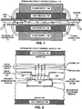
- FIG. 1 illustrates an integrated circuit assembly module 100 in accordance with one embodiment of the present invention.
- Integrated circuit assembly module 100 includes dies 102 (also referred to as "chips").
- Dies 102 are semiconductor dies that may include any type of computational circuitry, including main memory, cache memory, and processors. Dies 102 are arranged active face to active face and overlapped to facilitate capacitive communication between dies.
- Wafers 104 contain alignment structures that precisely position dies 102 to facilitate proximity communication.
- wafers 104 are silicon substrates that are comprised of the same material as dies 102.
- One of the two wafers in wafers 104 extends further than the other wafer in one dimension to allow for perimeter chips at the edges of integrated circuit assembly module 100 to extend beyond the opposite wafer.
- the exposed portions of the perimeter chips allow for external I/O connections via external I/O connectors 110.
- These external I/O connectors 110 can be electrical, optical, or any other type of connector that can be used to transfer data.
- heat removal devices 106 On the opposite sides of wafers 104 from dies 102 are heat removal devices 106, which may include any standard heat removal device such as heat sinks with fans.
- heat removal devices 106 can be made of a graphite foam (or other material, such as a metal) with fin-like structures that transfer heat to a liquid that is pumped through the graphite foam.
- Power supplies 108 are standard integrated circuit power supplies, and are attached to wafers 104 via power connectors 112.
- FIG. 2 illustrates a portion of an integrated circuit assembly module 100 with power connections in accordance with one embodiment of the present invention.
- Integrated circuit assembly module 100 contains metal planes that provide power 207 and ground 208 to dies 102 within integrated circuit assembly module 100, such as dies 204, 205, and 206. Since dies 204 to 206 are arranged with their active circuitry side facing each other, it is beneficial to connect power 207 and ground 208 to each chip from the wafer on the opposite side. For example, power 207 and ground 208 in wafer 202 can be attached to chip 204 via MEMS spring contacts 210. Similarly, power and ground for dies 205 and 206 can be provided through MEMS spring contacts from wafer 203.
- integrated circuit assembly module 100 is a complete self-contained system containing both memory and processor chips.
- external I/O connectors 110 can connect integrated circuit assembly module 100 to other computers or to other integrated circuit assembly modules.
- FIG. 3 presents various arrangements of chips to facilitate proximity communication between chips.
- Each pattern offers a different amount of overlap between chips. In some instances it may be better to maximize the overlap between chips, such as in a herringbone 302 or mosaic 306 pattern, while in other instances it may be better to maximize space between chips to facilitate heat removal, such as in a checkerboard 304 or tight checkerboard 308 pattern.
- Specific chip arrangements may prove to be optimal for specific types of chips. For instance, an integrated circuit module that contains only memory chips might utilize herringbone 302 as an optimal pattern, while an integrated circuit module that contains memory and processor chips might utilize checkerboard 304 as an optimal pattern.
Landscapes
- Semiconductor Integrated Circuits (AREA)
- Cooling Or The Like Of Semiconductors Or Solid State Devices (AREA)
- Lead Frames For Integrated Circuits (AREA)
Claims (18)
- Baugruppenmodul integrierter Schaltungen (100), das eine kapazitive Kommunikation zwischen Halbleiter-Chips unterstützt und das Folgendes umfasst:einen ersten Silizium-Wafer (104) mit einer Vorderseite und einer Rückseite gegenüber der Vorderseite;eine erste Schicht Halbleiter-Chips, wobei die erste Schicht Halbleiterchips einen ersten Halbleiter-Chip (102) mit einer aktiven Seite, auf der sich eine aktive Schaltung und Signalflächen befinden, und einer Rückseite gegenüber der aktiven Seite umfasst;eine zweite Schicht Halbleiter-Chips, wobei die zweite Schicht Halbleiter-Chips einen zweiten Halbleiter-Chip (102) mit einer aktiven Seite, auf der sich eine aktive Schaltung und Signalflächen befinden, und einer Rückseite gegenüber der aktiven Seite umfasst;einen zweiten Silizium-Wafer (104) mit einer Vorderseite und einer Rückseite gegenüber der Vorderseite;wobei der erste Halbleiter-Chip und der zweite Halbleiter-Chip mit einander zugewandten aktiven Seiten angeordnet sind, so dass die Signalflächen auf dem ersten Halbleiter-Chip die Signalflächen auf dem zweiten Halbleiter-Chip für eine kapazitive Kommunikation zwischen dem ersten Halbleiter-Chip und dem zweiten Halbleiter-Chip überdecken;wobei der erste Halbleiter-Chip und der zweite Halbleiter-Chip zwischen dem ersten Wafer und dem zweiten Wafer zusammengedrückt werden, so dass die Vorderseite des ersten Wafers mit der Rückseite des ersten Halbleiter-Chips in Kontakt ist und die Vorderseite des zweiten Wafers mit der Rückseite des zweiten Halbleiter-Chips in Kontakt ist;wobei das Baugruppenmodul integrierter Schaltungen ferner einen I/O-Halbleiter-Chip mit einer aktiven Seite, auf der sich eine aktive Schaltung und Signalflächen befinden, und einer Rückseite gegenüber der aktiven Fläche umfasst;wobei der I/O-Halbleiter-Chip und der zweite Halbleiter-Chip mit den aktiven Seiten zueinander angeordnet sind, so dass die Signalflächen auf dem I/O-Halbleiter-Chip die Signalflächen auf dem zweiten Halbleiter-Chip für eine kapazitive Kommunikation zwischen dem I/O-Halbleier-Chip und dem zweiten Halbleiter-Chip überdecken;wobei sich der I/O-Halbleiter-Chip auf einer Kante des ersten Wafers befindet, um das Liefern von Kommunikationen in das Baugruppenmodul integrierter Schaltungen hinein und aus ihm heraus zu erleichtern; undwobei sich die Kante des ersten Wafers über die Kante des zweiten Wafers hinaus erstreckt, so dass ein Teil der aktiven Seite des I/O-Halbleiter-Chips freiliegt, um externe Verbindungen zu erleichtern.
- Baugruppenmodul integrierter Schaltungen nach Anspruch 1, das ferner Folgendes umfasst:einen ersten Wärmeabführmechanismus (106), der an die Rückseite des ersten Wafers gekoppelt ist; undeinen zweiten Wärmeabführmechanismus (106), der an die Rückseite des zweiten Wafers gekoppelt ist.
- Baugruppenmodul integrierter Schaltungen nach Anspruch 2, wobei der erste und der zweite Wärmeabführmechanismus Kühlrippen enthalten, um eine Wärmeübertragung an Luft, die zwischen den Kühlrippen hindurchführt, zu erleichtern.
- Baugruppenmodul integrierter Schaltungen nach Anspruch 2, wobei der erste und der zweite Wärmeabführmechanismus Graphitschaum oder Metall mit rippenähnlichen Strukturen enthalten, die die Wärmeübertragung auf eine Flüssigkeit, die durch den Graphitschaum oder das Metall gepumpt wird, zu erleichtern.
- Baugruppenmodul integrierter Schaltungen nach einem vorhergehenden Anspruch, das ferner Folgendes umfasst:eine erste Stromversorgung (108), die an die Rückseite des ersten Wafers gekoppelt ist; undeine zweite Stromversorgung (108), die an die Rückseite des zweiten Wafers gekoppelt ist.
- Baugruppenmodul integrierter Schaltungen nach einem vorhergehenden Anspruch, wobei der erste und der zweite Wafer Metallschichten (207) enthalten, die Leistung an den ersten und den zweiten Halbleiter-Chip liefern.
- Baugruppenmodul integrierter Schaltungen nach Anspruch 6, wobei der erste und der zweite Wafer Netzanschlüsse auf den Rückseiten des ersten und des zweiten Wafers enthalten.
- Baugruppenmodul integrierter Schaltungen nach Anspruch 6 oder 7, das ferner Federkontakte eines mikroelektromechanischen Systems (MEMS) (210) umfasst, die Leistung von den Metallschichten innerhalb des ersten und des zweiten Wafers an den ersten und den zweiten Halbleiter-Chip liefern, wobei:eine erste Gruppe MEMS-Federkontakte auf der Vorderseite des ersten Wafers die aktive Seite des zweiten Halbleiter-Chips kontaktiert; undeine zweite Gruppe von MEMS-Federkontakten auf der Vorderseite des zweiten Wafers die aktive Seite des ersten Halbleiter-Chips kontaktiert.
- Baugruppenmodul integrierter Schaltungen nach einem der Ansprüche 6 bis 8, das ferner Folgendes umfasst:einen ersten Leistungsregulierer, der in den ersten Wafer eingebaut ist; undeinen zweiten Leistungsregulierer, der in den zweiten Wafer eingebaut ist.
- Baugruppenmodul integrierter Schaltungen nach Anspruch 1, das ferner optische externe Verbindungsflächen umfasst, die sich auf dem freiliegenden Teil der aktiven Seite des I/O-Halbleiter-Chips befinden.
- Baugruppenmodul integrierter Schaltungen nach Anspruch 1, das ferner elektrische externe Verbindungsflächen umfasst, die sich auf dem freiliegenden Teil der aktiven Seite des I/O-Halbleiter-Chips befinden.
- Verfahren zum Herstellen eines Baugruppenmoduls integrierter Schaltungen (100), das einen ersten und einen zweiten Halbleiter-Chip (102) enthält und eine kapazitive Kommunikation zwischen Halbleiter-Chips unterstützt, wobei der erste und der zweite Halbleiter-Chip eine aktive Seite, auf der sich eine aktive Schaltung und Signalflächen befinden, und eine Rückseite gegenüber der aktiven Seite umfassen, wobei das Verfahren Folgendes umfasst:Anordnen einer ersten Schicht Halbleiter-Chips, die den ersten Halbleiter-Chip enthält, und einer zweiten Schicht Halbleiter-Chips, die den zweiten Halbleiter-Chip enthält, mit einer zugewandten aktiven Seiten, so dass die Signalflächen auf dem ersten Halbleiter-Chip die Signalflächen auf dem zweiten Halbleiter-Chip für eine kapazitive Kommunikation zwischen dem ersten Halbleiter-Chip und dem zweiten Halbleiter-Chip überdecken; undZusammendrücken des ersten Halbleiter-Chips und des zweiten Halbleiter-Chips zwischen einen ersten Silizium-Wafer (104) und einen zweiten Silizium-Wafer (104), so dass der erste Wafer mit der Rückseite des ersten Halbleiter-Chips in Kontakt ist und der zweite Wafer mit der Rückseite des zweiten Halbleiter-Chips in Kontakt ist,wobei das Baugruppenmodul integrierter Schaltungen ferner Folgendes umfasst:einen I/O-Halbleiter-Chip mit einer aktiven Seite, auf der sich eine aktive Schaltung - einschließlich Signalflächen - befindet, und einer Rückseite gegenüber der aktiven Seite;wobei der I/O-Halbleiter-Chip und der zweite Halbleiter-Chip mit den aktiven Seiten zueinander angeordnet sind, so dass die Signalflächen auf dem I/O-Halbleiter-Chip die Signalflächen auf dem zweiten Halbleiter-Chip überdecken, wodurch eine kapazitive Kommunikation zwischen dem I/O-Halbleiter-Chip und dem zweiten Halbleiter-Chip erleichtert wird;wobei sich der I/O-Halbleiter-Chip auf der Kante des ersten Wafers befindet, um das Liefern von Kommunikationen in das Baugruppenmodul integrierter Schaltungen hinein und aus ihm heraus zu erleichtern; undwobei sich die Kante des ersten Wafers über die Kante des zweiten Wafers hinaus erstreckt, so dass ein Teil der aktiven Seite des I/O-Halbleiter-Chips freiliegt, um externe Verbindungen zu erleichtern.
- Verfahren nach Anspruch 12, wobei das Baugruppenmodul integrierter Schaltungen ferner Folgendes umfasst:einen ersten Wärmeabführmechanismus (106), der an die dem ersten Halbleiter-Chip gegenüberliegende Seite des ersten Wafers gekoppelt ist; undeinen zweiten Wärmeabführmechanismus (106), der an die dem zweiten Halbleiter-Chip gegenüberliegende Seite des zweiten Wafers gekoppelt ist.
- Verfahren nach Anspruch 12 oder 13, wobei das Baugruppenmodul integrierter Schaltungen ferner Folgendes umfasst:eine erste Stromversorgung (108), die an die dem ersten Halbleiter-Chip gegenüberliegende Seite des ersten Wafers gekoppelt ist; undeine zweite Stromversorgung (108), die an die dem zweiten Halbleiter-Chip gegenüberliegende Seite des zweiten Wafers gekoppelt ist.
- Verfahren nach einem der Ansprüche 12 bis 14, wobei der erste und der zweite Wafer Metallschichten (207) enthalten, die die Versorgung des ersten und des zweiten Halbleiter-Chips mit Leistung erleichtern.
- Verfahren nach Anspruch 15, wobei der erste und der zweite Wafer auf den Seiten des ersten und des zweiten Wafers, die dem ersten und dem zweiten Halbleiter-Chip gegenüberliegen, Netzanschlüsse enthalten.
- Verfahren nach Anspruch 15 oder 16, wobei das Baugruppenmodul integrierter Schaltungen ferner Federkontakte eines mikroelektromechanischen Systems (MEMS) (210) umfassen, die das Liefern von Leistung von den Metallschichten innerhalb des ersten und des zweiten Wafers an den ersten und den zweiten Halbleiter-Chip erleichtern, und wobei:mehrere erste MEMS-Federkontakte, die an der Seite des Halbleiter-Chips des ersten Wafers angebracht sind, die aktive Seite des zweiten Halbleiter-Chips kontaktieren; undmehrere zweite MEMS-Federkontakte, die an der Seite des Halbleiter-Chips des zweiten Wafers angebracht sind, die aktive Seite des ersten Halbleiter-Chips kontaktieren.
- Computersystem, das ein Baugruppenmodul integrierter Schaltungen nach einem der Ansprüche 1 bis 11 umfasst.
Applications Claiming Priority (4)
| Application Number | Priority Date | Filing Date | Title |
|---|---|---|---|
| US44380803P | 2003-01-29 | 2003-01-29 | |
| US443808P | 2003-01-29 | ||
| US10/671,642 US6870271B2 (en) | 2003-01-29 | 2003-09-26 | Integrated circuit assembly module that supports capacitive communication between semiconductor dies |
| US671642 | 2003-09-26 |
Publications (3)
| Publication Number | Publication Date |
|---|---|
| EP1443559A2 EP1443559A2 (de) | 2004-08-04 |
| EP1443559A3 EP1443559A3 (de) | 2008-07-09 |
| EP1443559B1 true EP1443559B1 (de) | 2017-05-03 |
Family
ID=32659512
Family Applications (1)
| Application Number | Title | Priority Date | Filing Date |
|---|---|---|---|
| EP04250054.6A Expired - Lifetime EP1443559B1 (de) | 2003-01-29 | 2004-01-07 | Modul mit Anordnung integrierter Schaltungen |
Country Status (4)
| Country | Link |
|---|---|
| US (1) | US6870271B2 (de) |
| EP (1) | EP1443559B1 (de) |
| JP (1) | JP4444681B2 (de) |
| TW (1) | TWI313052B (de) |
Families Citing this family (28)
| Publication number | Priority date | Publication date | Assignee | Title |
|---|---|---|---|---|
| US7612443B1 (en) | 2003-09-04 | 2009-11-03 | University Of Notre Dame Du Lac | Inter-chip communication |
| US7067910B2 (en) * | 2004-04-13 | 2006-06-27 | Sun Microsystems, Inc. | Method and apparatus for using capacitively coupled communication within stacks of laminated chips |
| US7525199B1 (en) * | 2004-05-21 | 2009-04-28 | Sun Microsystems, Inc | Packaging for proximity communication positioned integrated circuits |
| WO2006011960A1 (en) * | 2004-06-25 | 2006-02-02 | Sun Microsystems, Inc. | Integrated circuit chip that supports through-chip electromagnetic communication |
| US7175445B2 (en) * | 2004-08-31 | 2007-02-13 | Tyco Electronics Corporation | Electrical connector power wafers |
| US7106079B2 (en) * | 2004-10-22 | 2006-09-12 | Sun Microsystems, Inc. | Using an interposer to facilate capacitive communication between face-to-face chips |
| JP2006190972A (ja) * | 2004-12-08 | 2006-07-20 | Mitsubishi Electric Corp | 電力用半導体装置 |
| EP1701384A1 (de) * | 2005-03-08 | 2006-09-13 | Sun Microsystems France S.A. | Netzwerkplanung mit Halbleiterchips für Gitternetzkommunikation |
| US7573720B1 (en) * | 2005-06-15 | 2009-08-11 | Sun Microsystems, Inc. | Active socket for facilitating proximity communication |
| EP1963638A2 (de) * | 2005-12-22 | 2008-09-03 | Econox Technologies, LLC | Vorrichtung und verfahren für brennstoffdurchfluss, brennstofftemperatur, brennstofftröpfchengrösse sowie brenner-brennratenmodulation |
| US7356213B1 (en) * | 2006-03-28 | 2008-04-08 | Sun Microsystems, Inc. | Transparent switch using optical and electrical proximity communication |
| US7949436B2 (en) * | 2006-05-19 | 2011-05-24 | Oracle America, Inc. | Method and apparatus for automatically detecting and correcting misalignment of a semiconductor chip |
| US7893531B2 (en) * | 2007-09-28 | 2011-02-22 | Oracle America, Inc. | Integrated-circuit package for proximity communication |
| US8396136B1 (en) | 2009-07-22 | 2013-03-12 | The United States Of America As Represented By The Secretary Of The Navy | Close-proximity communications system using capacitively coupled signal transfer |
| US8164917B2 (en) * | 2009-12-23 | 2012-04-24 | Oracle America, Inc. | Base plate for use in a multi-chip module |
| US8340576B2 (en) * | 2010-06-29 | 2012-12-25 | Stmicroelectronics S.R.L. | Electronic circuit for communicating through capacitive coupling |
| US8150315B2 (en) * | 2010-06-29 | 2012-04-03 | Stmicroelectronics S.R.L. | Method for verifying the alignment between integrated electronic devices |
| US9147636B2 (en) | 2011-06-29 | 2015-09-29 | Stmicroelectronics S.R.L. | Method for verifying the alignment between integrated electronic devices |
| US8704364B2 (en) * | 2012-02-08 | 2014-04-22 | Xilinx, Inc. | Reducing stress in multi-die integrated circuit structures |
| US8704384B2 (en) | 2012-02-17 | 2014-04-22 | Xilinx, Inc. | Stacked die assembly |
| US8957512B2 (en) | 2012-06-19 | 2015-02-17 | Xilinx, Inc. | Oversized interposer |
| US8869088B1 (en) | 2012-06-27 | 2014-10-21 | Xilinx, Inc. | Oversized interposer formed from a multi-pattern region mask |
| US9026872B2 (en) | 2012-08-16 | 2015-05-05 | Xilinx, Inc. | Flexible sized die for use in multi-die integrated circuit |
| US9620473B1 (en) | 2013-01-18 | 2017-04-11 | University Of Notre Dame Du Lac | Quilt packaging system with interdigitated interconnecting nodules for inter-chip alignment |
| US9041220B2 (en) | 2013-02-13 | 2015-05-26 | Qualcomm Incorporated | Semiconductor device having stacked memory elements and method of stacking memory elements on a semiconductor device |
| US9547034B2 (en) | 2013-07-03 | 2017-01-17 | Xilinx, Inc. | Monolithic integrated circuit die having modular die regions stitched together |
| US9915869B1 (en) | 2014-07-01 | 2018-03-13 | Xilinx, Inc. | Single mask set used for interposer fabrication of multiple products |
| US10410950B1 (en) * | 2018-05-11 | 2019-09-10 | Micron Technology, Inc. | Heat spreaders for use with semiconductor devices |
Family Cites Families (11)
| Publication number | Priority date | Publication date | Assignee | Title |
|---|---|---|---|---|
| US4467342A (en) * | 1982-07-15 | 1984-08-21 | Rca Corporation | Multi-chip imager |
| US5491612A (en) * | 1995-02-21 | 1996-02-13 | Fairchild Space And Defense Corporation | Three-dimensional modular assembly of integrated circuits |
| US5567657A (en) * | 1995-12-04 | 1996-10-22 | General Electric Company | Fabrication and structures of two-sided molded circuit modules with flexible interconnect layers |
| JP3937265B2 (ja) * | 1997-09-29 | 2007-06-27 | エルピーダメモリ株式会社 | 半導体装置 |
| SG93192A1 (en) * | 1999-01-28 | 2002-12-17 | United Microelectronics Corp | Face-to-face multi chip package |
| US6559531B1 (en) | 1999-10-14 | 2003-05-06 | Sun Microsystems, Inc. | Face to face chips |
| KR100335717B1 (ko) * | 2000-02-18 | 2002-05-08 | 윤종용 | 고용량 메모리 카드 |
| US6586836B1 (en) * | 2000-03-01 | 2003-07-01 | Intel Corporation | Process for forming microelectronic packages and intermediate structures formed therewith |
| US6507115B2 (en) * | 2000-12-14 | 2003-01-14 | International Business Machines Corporation | Multi-chip integrated circuit module |
| US6495396B1 (en) | 2001-08-29 | 2002-12-17 | Sun Microsystems, Inc. | Method of coupling and aligning semiconductor devices including multi-chip semiconductor devices |
| US6555917B1 (en) * | 2001-10-09 | 2003-04-29 | Amkor Technology, Inc. | Semiconductor package having stacked semiconductor chips and method of making the same |
-
2003
- 2003-09-26 US US10/671,642 patent/US6870271B2/en not_active Expired - Lifetime
-
2004
- 2004-01-07 EP EP04250054.6A patent/EP1443559B1/de not_active Expired - Lifetime
- 2004-01-28 JP JP2004020598A patent/JP4444681B2/ja not_active Expired - Lifetime
- 2004-01-29 TW TW093102044A patent/TWI313052B/zh not_active IP Right Cessation
Also Published As
| Publication number | Publication date |
|---|---|
| EP1443559A3 (de) | 2008-07-09 |
| JP4444681B2 (ja) | 2010-03-31 |
| TWI313052B (en) | 2009-08-01 |
| US20040145063A1 (en) | 2004-07-29 |
| TW200416978A (en) | 2004-09-01 |
| EP1443559A2 (de) | 2004-08-04 |
| US6870271B2 (en) | 2005-03-22 |
| JP2004235644A (ja) | 2004-08-19 |
Similar Documents
| Publication | Publication Date | Title |
|---|---|---|
| EP1443559B1 (de) | Modul mit Anordnung integrierter Schaltungen | |
| EP2609623B1 (de) | Optische kommunikation in einem ramp-stack-chipgehäuse | |
| TWI527132B (zh) | 晶片封裝,電子計算裝置及用以傳遞信號之方法 | |
| CN102484108B (zh) | 高带宽倾斜叠层芯片封装 | |
| US20060095639A1 (en) | Structures and methods for proximity communication using bridge chips | |
| US20070210446A1 (en) | Apparatus and Methods For Cooling Semiconductor Integrated Circuit Chip Packages | |
| US7888175B2 (en) | Method and apparatus for facilitating proximity communication and power delivery | |
| WO1993007659A1 (en) | Direct integrated circuit interconnection system | |
| EP2201602A1 (de) | Ausrichtungsmerkmale für die proximitätskommunikation | |
| US7638884B2 (en) | Thin semiconductor device package | |
| CN113299632A (zh) | 具有镜像电路的堆叠式晶粒的集成电路器件 | |
| US7396763B2 (en) | Semiconductor package using flexible film and method of manufacturing the same | |
| US8166644B2 (en) | Method for manufacturing an active socket for facilitating proximity communication | |
| JP2000269545A (ja) | 光電子集積回路装置 | |
| US8026598B2 (en) | Semiconductor chip module with stacked flip-chip unit | |
| KR100225398B1 (ko) | 반도체 범프의 본딩구조 및 방법 | |
| US6958538B1 (en) | Computer system architecture using a proximity I/O switch | |
| US7170121B1 (en) | Computer system architecture using a proximity I/O switch | |
| US6326647B1 (en) | Packaging and mounting of spherical semiconductor devices | |
| CN101359600B (zh) | 用于细间距基板的集成电路封装件系统 | |
| TWI918629B (zh) | 具有鏡像電路系統的堆疊式晶粒的積體電路裝置及其製造方法 | |
| CN116033673A (zh) | 电路板级封装方法及电路板 |
Legal Events
| Date | Code | Title | Description |
|---|---|---|---|
| PUAI | Public reference made under article 153(3) epc to a published international application that has entered the european phase |
Free format text: ORIGINAL CODE: 0009012 |
|
| AK | Designated contracting states |
Kind code of ref document: A2 Designated state(s): AT BE BG CH CY CZ DE DK EE ES FI FR GB GR HU IE IT LI LU MC NL PT RO SE SI SK TR |
|
| AX | Request for extension of the european patent |
Extension state: AL LT LV MK |
|
| PUAL | Search report despatched |
Free format text: ORIGINAL CODE: 0009013 |
|
| AK | Designated contracting states |
Kind code of ref document: A3 Designated state(s): AT BE BG CH CY CZ DE DK EE ES FI FR GB GR HU IE IT LI LU MC NL PT RO SE SI SK TR |
|
| AX | Request for extension of the european patent |
Extension state: AL LT LV MK |
|
| 17P | Request for examination filed |
Effective date: 20081009 |
|
| AKX | Designation fees paid |
Designated state(s): DE GB |
|
| RAP1 | Party data changed (applicant data changed or rights of an application transferred) |
Owner name: ORACLE AMERICA, INC. |
|
| 17Q | First examination report despatched |
Effective date: 20110228 |
|
| REG | Reference to a national code |
Ref country code: DE Ref legal event code: R079 Ref document number: 602004051184 Country of ref document: DE Free format text: PREVIOUS MAIN CLASS: H01L0025065000 Ipc: H01L0023367000 |
|
| RIC1 | Information provided on ipc code assigned before grant |
Ipc: H01L 23/367 20060101AFI20160929BHEP Ipc: H01L 23/473 20060101ALN20160929BHEP Ipc: H01L 25/065 20060101ALI20160929BHEP Ipc: H01L 23/48 20060101ALI20160929BHEP |
|
| GRAP | Despatch of communication of intention to grant a patent |
Free format text: ORIGINAL CODE: EPIDOSNIGR1 |
|
| STAA | Information on the status of an ep patent application or granted ep patent |
Free format text: STATUS: GRANT OF PATENT IS INTENDED |
|
| INTG | Intention to grant announced |
Effective date: 20161124 |
|
| GRAS | Grant fee paid |
Free format text: ORIGINAL CODE: EPIDOSNIGR3 |
|
| GRAA | (expected) grant |
Free format text: ORIGINAL CODE: 0009210 |
|
| STAA | Information on the status of an ep patent application or granted ep patent |
Free format text: STATUS: THE PATENT HAS BEEN GRANTED |
|
| AK | Designated contracting states |
Kind code of ref document: B1 Designated state(s): DE GB |
|
| REG | Reference to a national code |
Ref country code: GB Ref legal event code: FG4D |
|
| REG | Reference to a national code |
Ref country code: DE Ref legal event code: R096 Ref document number: 602004051184 Country of ref document: DE |
|
| REG | Reference to a national code |
Ref country code: DE Ref legal event code: R097 Ref document number: 602004051184 Country of ref document: DE |
|
| PLBE | No opposition filed within time limit |
Free format text: ORIGINAL CODE: 0009261 |
|
| STAA | Information on the status of an ep patent application or granted ep patent |
Free format text: STATUS: NO OPPOSITION FILED WITHIN TIME LIMIT |
|
| 26N | No opposition filed |
Effective date: 20180206 |
|
| REG | Reference to a national code |
Ref country code: DE Ref legal event code: R082 Ref document number: 602004051184 Country of ref document: DE Representative=s name: D YOUNG & CO LLP, DE |
|
| PGFP | Annual fee paid to national office [announced via postgrant information from national office to epo] |
Ref country code: GB Payment date: 20221201 Year of fee payment: 20 |
|
| PGFP | Annual fee paid to national office [announced via postgrant information from national office to epo] |
Ref country code: DE Payment date: 20221130 Year of fee payment: 20 |
|
| P01 | Opt-out of the competence of the unified patent court (upc) registered |
Effective date: 20230522 |
|
| REG | Reference to a national code |
Ref country code: DE Ref legal event code: R071 Ref document number: 602004051184 Country of ref document: DE |
|
| REG | Reference to a national code |
Ref country code: GB Ref legal event code: PE20 Expiry date: 20240106 |
|
| PG25 | Lapsed in a contracting state [announced via postgrant information from national office to epo] |
Ref country code: GB Free format text: LAPSE BECAUSE OF EXPIRATION OF PROTECTION Effective date: 20240106 |