EP1444724B1 - Procede de structuration photolithographique au moyen d'une couche masque dure, de durete analogue au diamant, obtenue par depot assiste au plasma - Google Patents
Procede de structuration photolithographique au moyen d'une couche masque dure, de durete analogue au diamant, obtenue par depot assiste au plasma Download PDFInfo
- Publication number
- EP1444724B1 EP1444724B1 EP02776865A EP02776865A EP1444724B1 EP 1444724 B1 EP1444724 B1 EP 1444724B1 EP 02776865 A EP02776865 A EP 02776865A EP 02776865 A EP02776865 A EP 02776865A EP 1444724 B1 EP1444724 B1 EP 1444724B1
- Authority
- EP
- European Patent Office
- Prior art keywords
- hard mask
- layer
- mask layer
- carbon hard
- process according
- Prior art date
- Legal status (The legal status is an assumption and is not a legal conclusion. Google has not performed a legal analysis and makes no representation as to the accuracy of the status listed.)
- Expired - Lifetime
Links
Images


Classifications
-
- H—ELECTRICITY
- H10—SEMICONDUCTOR DEVICES; ELECTRIC SOLID-STATE DEVICES NOT OTHERWISE PROVIDED FOR
- H10P—GENERIC PROCESSES OR APPARATUS FOR THE MANUFACTURE OR TREATMENT OF DEVICES COVERED BY CLASS H10
- H10P14/00—Formation of materials, e.g. in the shape of layers or pillars
- H10P14/60—Formation of materials, e.g. in the shape of layers or pillars of insulating materials
- H10P14/69—Inorganic materials
- H10P14/6902—Inorganic materials composed of carbon, e.g. alpha-C, diamond or hydrogen doped carbon
-
- G—PHYSICS
- G03—PHOTOGRAPHY; CINEMATOGRAPHY; ANALOGOUS TECHNIQUES USING WAVES OTHER THAN OPTICAL WAVES; ELECTROGRAPHY; HOLOGRAPHY
- G03F—PHOTOMECHANICAL PRODUCTION OF TEXTURED OR PATTERNED SURFACES, e.g. FOR PRINTING, FOR PROCESSING OF SEMICONDUCTOR DEVICES; MATERIALS THEREFOR; ORIGINALS THEREFOR; APPARATUS SPECIALLY ADAPTED THEREFOR
- G03F7/00—Photomechanical, e.g. photolithographic, production of textured or patterned surfaces, e.g. printing surfaces; Materials therefor, e.g. comprising photoresists; Apparatus specially adapted therefor
- G03F7/26—Processing photosensitive materials; Apparatus therefor
- G03F7/40—Treatment after imagewise removal, e.g. baking
-
- H—ELECTRICITY
- H10—SEMICONDUCTOR DEVICES; ELECTRIC SOLID-STATE DEVICES NOT OTHERWISE PROVIDED FOR
- H10P—GENERIC PROCESSES OR APPARATUS FOR THE MANUFACTURE OR TREATMENT OF DEVICES COVERED BY CLASS H10
- H10P14/00—Formation of materials, e.g. in the shape of layers or pillars
- H10P14/60—Formation of materials, e.g. in the shape of layers or pillars of insulating materials
-
- H—ELECTRICITY
- H10—SEMICONDUCTOR DEVICES; ELECTRIC SOLID-STATE DEVICES NOT OTHERWISE PROVIDED FOR
- H10P—GENERIC PROCESSES OR APPARATUS FOR THE MANUFACTURE OR TREATMENT OF DEVICES COVERED BY CLASS H10
- H10P14/00—Formation of materials, e.g. in the shape of layers or pillars
- H10P14/60—Formation of materials, e.g. in the shape of layers or pillars of insulating materials
- H10P14/66—Formation of materials, e.g. in the shape of layers or pillars of insulating materials characterised by the type of materials
- H10P14/668—Formation of materials, e.g. in the shape of layers or pillars of insulating materials characterised by the type of materials the materials being characterised by the deposition precursor materials
-
- H—ELECTRICITY
- H10—SEMICONDUCTOR DEVICES; ELECTRIC SOLID-STATE DEVICES NOT OTHERWISE PROVIDED FOR
- H10P—GENERIC PROCESSES OR APPARATUS FOR THE MANUFACTURE OR TREATMENT OF DEVICES COVERED BY CLASS H10
- H10P50/00—Etching of wafers, substrates or parts of devices
- H10P50/69—Etching of wafers, substrates or parts of devices using masks for semiconductor materials
- H10P50/691—Etching of wafers, substrates or parts of devices using masks for semiconductor materials for Group V materials or Group III-V materials
- H10P50/692—Etching of wafers, substrates or parts of devices using masks for semiconductor materials for Group V materials or Group III-V materials characterised by their composition, e.g. multilayer masks or materials
-
- H—ELECTRICITY
- H10—SEMICONDUCTOR DEVICES; ELECTRIC SOLID-STATE DEVICES NOT OTHERWISE PROVIDED FOR
- H10P—GENERIC PROCESSES OR APPARATUS FOR THE MANUFACTURE OR TREATMENT OF DEVICES COVERED BY CLASS H10
- H10P50/00—Etching of wafers, substrates or parts of devices
- H10P50/73—Etching of wafers, substrates or parts of devices using masks for insulating materials
-
- H—ELECTRICITY
- H10—SEMICONDUCTOR DEVICES; ELECTRIC SOLID-STATE DEVICES NOT OTHERWISE PROVIDED FOR
- H10P—GENERIC PROCESSES OR APPARATUS FOR THE MANUFACTURE OR TREATMENT OF DEVICES COVERED BY CLASS H10
- H10P76/00—Manufacture or treatment of masks on semiconductor bodies, e.g. by lithography or photolithography
- H10P76/20—Manufacture or treatment of masks on semiconductor bodies, e.g. by lithography or photolithography of masks comprising organic materials
-
- H—ELECTRICITY
- H10—SEMICONDUCTOR DEVICES; ELECTRIC SOLID-STATE DEVICES NOT OTHERWISE PROVIDED FOR
- H10P—GENERIC PROCESSES OR APPARATUS FOR THE MANUFACTURE OR TREATMENT OF DEVICES COVERED BY CLASS H10
- H10P76/00—Manufacture or treatment of masks on semiconductor bodies, e.g. by lithography or photolithography
- H10P76/40—Manufacture or treatment of masks on semiconductor bodies, e.g. by lithography or photolithography of masks comprising inorganic materials
- H10P76/405—Manufacture or treatment of masks on semiconductor bodies, e.g. by lithography or photolithography of masks comprising inorganic materials characterised by their composition, e.g. multilayer masks
-
- H—ELECTRICITY
- H10—SEMICONDUCTOR DEVICES; ELECTRIC SOLID-STATE DEVICES NOT OTHERWISE PROVIDED FOR
- H10P—GENERIC PROCESSES OR APPARATUS FOR THE MANUFACTURE OR TREATMENT OF DEVICES COVERED BY CLASS H10
- H10P14/00—Formation of materials, e.g. in the shape of layers or pillars
- H10P14/60—Formation of materials, e.g. in the shape of layers or pillars of insulating materials
- H10P14/63—Formation of materials, e.g. in the shape of layers or pillars of insulating materials characterised by the formation processes
- H10P14/6326—Deposition processes
- H10P14/6328—Deposition from the gas or vapour phase
- H10P14/6334—Deposition from the gas or vapour phase using decomposition or reaction of gaseous or vapour phase compounds, i.e. chemical vapour deposition
- H10P14/6336—Deposition from the gas or vapour phase using decomposition or reaction of gaseous or vapour phase compounds, i.e. chemical vapour deposition in the presence of a plasma [PECVD]
-
- H—ELECTRICITY
- H10—SEMICONDUCTOR DEVICES; ELECTRIC SOLID-STATE DEVICES NOT OTHERWISE PROVIDED FOR
- H10P—GENERIC PROCESSES OR APPARATUS FOR THE MANUFACTURE OR TREATMENT OF DEVICES COVERED BY CLASS H10
- H10P14/00—Formation of materials, e.g. in the shape of layers or pillars
- H10P14/60—Formation of materials, e.g. in the shape of layers or pillars of insulating materials
- H10P14/69—Inorganic materials
- H10P14/692—Inorganic materials composed of oxides, glassy oxides or oxide-based glasses
- H10P14/6921—Inorganic materials composed of oxides, glassy oxides or oxide-based glasses containing silicon
- H10P14/6922—Inorganic materials composed of oxides, glassy oxides or oxide-based glasses containing silicon the material containing Si, O and at least one of H, N, C, F or other non-metal elements, e.g. SiOC, SiOC:H or SiONC
- H10P14/6927—Inorganic materials composed of oxides, glassy oxides or oxide-based glasses containing silicon the material containing Si, O and at least one of H, N, C, F or other non-metal elements, e.g. SiOC, SiOC:H or SiONC the material being a silicon oxynitride, e.g. SiON or SiON:H
Definitions
- the present invention generally relates to the field of structuring methods for semiconductor technology in which a layer is to be patterned on the surface of a substrate.
- the invention relates to a structuring method according to the preamble of patent claim 1.
- a process step in which the portions to be removed are at least partially formed by a silicon oxide or silicon nitride.
- An example of this is the production of semiconductor memory cells having a trench capacitor and a selection transistor. While the trench capacitor is electrically connected on one side to the selection transistor by a buried strap, a shallow trench isolation (STI) is produced on the other side of the trench capacitor, through which the trench capacitor from an adjacent one Memory cell is electrically isolated.
- the generation of the STI isolation region is performed by a patterning step in which a surface portion formed by a portion of the trench capacitor previously formed is removed.
- the said process of generating the STI isolation region places the highest demands on the positional accuracy, dimensional accuracy and edge steepness of the etching process to be used, since the edge to be etched is the one to be etched Deepening with extremely low lateral positional error within the trench capacitor must be located on the side facing away from the line bridge.
- the reflection of light of the exposure wavelength at the wafer surface is prevented as completely as possible eliminate interfering interference effects. This is especially true for exposure wavelengths at and below 248 nm (193 nm, 157 nm) due to the increasing reflectivity of the substrates.
- the lacquer layer to be exposed on the one hand has to be as thin as possible on the one hand.
- a sufficient mask thickness and / or a high etch resistance of the mask is necessary.
- EP 0 492 253 A1 describes a photostructuring method in which two photoresist layers are used.
- An upper, relatively thin photoresist layer (top resist) is made resistant to dry etching in oxygen plasma after structuring with a silicon-containing agent.
- the top-resist structure is transferred to a lower, relatively thick photoresist layer (bottom resist) with the exact amount of mask used for patterning and with vertical edges.
- CARL Chemical Expansion of Resist Lines
- the bottom resist serves as the actual mask during the etching of the substrate.
- the bottom resist itself must then be removed in a special etching process, for example with O 2 or SO 2 .
- a special etching process for example with O 2 or SO 2 .
- Such photoresist masks have the decisive disadvantage, in particular during the etching of contact holes with a very high aspect ratio, that the polymers resulting from the resist during the etching can not be controlled. This can lead to a strong reduction of the etching process window for very small structures.
- a so-called hard mask is used as the auxiliary layer.
- a photoresist layer is exposed on a mask layer of a silicon-containing dielectric according to a predetermined structure and patterned using solvent.
- the photoresist layer is used to transfer the structure into the mask layer using a modified anisotropic plasma etching process in which the chemical portion of the etch is dominant.
- the photoresist and the patterned mask layer may be used as a mask for a dry etching process to pattern the substrate.
- hardmasks made of polysilicon are used.
- the Polysilicon hard mask layer is thereby deposited in a furnace process at temperatures between 600 ° C and 700 ° C, which may cause problems due to the heat load of the circuit structures already generated.
- a general problem of the aforementioned hard mask materials is that they must be opened in a special etching step.
- Another disadvantage is that they are mostly - as in the example polysilicon - not suitable as anti-reflective layers.
- anti-reflective organic layers are known, which are brought by spin coating method before the actual coating with the exposed photoresist with a track on the surface of the wafer.
- these layers can not be used as hard mask layers and the reflection can only be reduced to about 10%.
- inorganic oxynitrides which are applied by a CVD method are known as antireflecting layers, whereby the reflection can not be reduced below 10%. At least for use in oxide etching processes, these layers are also not suitable as hard mask layers.
- the preparation of the carbon hard mask layer by the PECVD method gives good results as long as the deposition can be done on planar structures.
- the PECVD method involves the disadvantage that the carbon layer is not optimally filled in the trenches and holes and also has no planarizing effect.
- Another disadvantage is that in general the hardmask quality of the carbon hardmask layer increases with increasing hardness, ie increasing diamond content, in the layer and with decreasing hydrogen content, but both criteria can only be realized to a limited extent with the PECVD process. For example, the diamond content of layers deposited with PECVD is nearly zero and the hydrogen content can not be reduced below 15%.
- US Pat. No. 5,981,398 describes a structuring process using a chlorine-containing plasma using a hard mask.
- hard mask material inter alia, an amorphous carbon layer is described, which is produced by a HDP (high density plasma) CVD method.
- the etching processes described therein serve for the production and structuring of electrically conductive materials, in particular (A1-) trace materials.
- A1- electrically conductive materials
- An essential idea of the invention is to deposit the carbon hard mask layer by a plasma-assisted deposition method and to carry out the deposition in such a way that the carbon hard mask layer has a hardness comparable to a diamond in at least one layer thickness section.
- the said layer thickness section extends over the entire carbon hard mask layer and thus the carbon hard mask layer has optimum diamond-like hardness properties and etching resistance properties over its entire thickness.
- the layer has a diamond-like hardness only in a limited layer thickness section and has a different hardness in the remaining layer thickness sections.
- the terms "diamond-like” or “graphite-like” are used frequently, this does not apply necessarily on the structure of the applied layer. Even if the layer of diamond-like hardness is applied, the crystal structure can and will usually be an amorphous carbon structure.
- the parameters are set according to the invention in the deposition such that regions resulting graphitically are removed again in situ by subsequent etching processes and that only areas that arise like diamonds remain.
- Such parameters which promote the etching processes are, for example, the supply of ionizable gases such as argon and / or neon into the reactor chamber, by means of which additional ion bombardment is brought about in the deposition.
- Another parameter promoting the etching processes is the hydrogen content in the gas phase.
- the structuring process can be carried out by first applying a carbon hard mask layer to the substrate to be structured as indicated, and then applying a photoresist layer to the carbon hard mask layer. After exposing and developing the photoresist layer to form a predetermined pattern, this structure is transferred into the carbon hardmask layer. The carbon hard mask layer then serves as the actual etching mask for etching the substrate.
- the carbon hard mask layer is patterned via an etch-resistant intermediate layer, which may be formed, for example, by a silicon oxide nitride layer.
- HDP high density plasma
- the HDP deposition may be performed at pressures of about 0.133 - 26.6 Pa and the substrate temperature may be controlled in a range between 200 ° C - 750 ° C, preferably 600 ° C - 750 ° C.
- An HDP reactor for producing a high density plasma includes a central chamber in which semiconductor or insulator substrates sit on a boat that does not interfere with the substrates or introduce any contaminants into the substrates.
- the central chamber is made of a material that can withstand pressures less than or equal to 1 mTorr or less, at such pressures, minimizing outgassing and no impurities entering the interior of the chamber or into the substrates or a thin film thereon penetration.
- the central chamber operates at an operating pressure much lower than conventional gas phase chemical vapor deposition chambers or plasma enhanced chemical vapor deposition.
- the pressure within the chamber is about 0.67 Pa (5 mTorr), while plasma assisted chemical vapor deposition typically uses a pressure of about 267 Pa (2 Torr).
- the plasma density within the chamber is much higher than the normal chemical vapor deposition, even when plasma enhanced, and is preferably above 10 16 ions / m 3 , preferably in the range of 10 16 to 10 22, and more preferably in the range of 10 17 to 10 19 ions / m 3 .
- the plasma density could be even higher.
- the plasma density is in the range of 10 14 to 10 16 ions / m 3 .
- a characteristic of the method according to the invention is that the material deposition is superimposed on an ion sputter etching. This contribution should be so large that, as already indicated, a growth selection process is emerging.
- the layer can be sputtered with Ar ions, Ne ions or other ions.
- Suitable carbon precursors are gases such as CH 4 , C 2 H 6 , C 2 H 4 , C 2 H 2 and C 3 H 6 .
- Also advantageous for the formation of layers is the addition of relatively large amounts of hydrogen.
- the carbon layers produced become harder, because both parameters require etching of the graphite-like portions in the carbon layer, whereby the simultaneously present diamond portions are not etched back because they are more resistant to this attack.
- the layer thus formed is more resistant to ion etching processes and thus gives a higher quality hardmask.
- the simultaneous deposition-sputtering process enables filling of trenches or holes on structured surfaces.
- the carbon layer deposited by the HDP method has a lower hydrogen content than the carbon layer deposited by the PECVD method.
- the hydrogen content can be reduced to less than 5%.
- the carbon layer fills without cavities in the smallest structures with diameters below 100 nm and is able to planarize topographies.
- Both the ion bombardment and the substrate temperature can be selectively varied during the deposition. Thereby the formation of so-called gradient layers is possible, ie with the layer depth, the optical properties and also the mechanical properties can be changed. As a result, optimal antireflecting layers are produced, since a change in the refractive index with the layer depth means a maximum reflection reduction.
- the process can be designed so that the hardness is greater, for example, in the lowest layer areas than at the layer surface. This enables optimal process control during the subsequent dry etching process.
- a PECVD (plasma enhanced chemical vapor deposition) deposition method can be selected. It is a prerequisite that the electrode of the commonly used parallel plate reactor, on which the substrates are arranged, is connected as a cathode. In this case, part of the growing layer is sputtered away by the ions again.
- elements such as argon, neon and the like can be used as in the HDP deposition process. be supplied to the reactor to a greater extent to form corresponding ions.
- the described method of using a carbon hardmask layer can also be combined with the CARL process described in the introduction, in which chemical amplification of the photoresist layer resist lines is brought about.
- This chemical amplification can be effected, for example, by a wet-chemical silylation, that is to say the addition of silyl groups to the organic resist material, as has been described, for example, in the publications DE 42 26 464, EP 0 395 917 or US Pat. No. 5,234,793.
- the method according to the invention is particularly suitable for producing the trench isolation already described above in the production of memory cells with trench capacitor and selection transistor by the so-called AA process (active area).
- AA process active area
- a borosilicate glass hard mask is currently being used as an etching mask, which for various reasons is not an optimal solution.
- a substrate 1 to be structured is provided, which may, for example, be a chip or wafer in which a matrix-shaped arrangement of trench capacitors has already been processed, which are each associated with memory cells.
- isolation regions are to be generated between the trench capacitors. Since the sections to be removed for generating the isolation regions also each contain subsections of the processed trench capacitors, silicon oxide also has to be etched, since the trench capacitors generally have an insulation collar made of silicon oxide.
- a carbon hard mask layer 2 is first applied on the thus pre-processed substrate 1.
- the production of the carbon hard mask layer 2 takes place as described by a plasma-assisted deposition process.
- there is generally a topographical structure in which it is advantageous to choose an HDP method for the deposition of the carbon hard mask layer 2, so that the carbon fills in all existing trenches and holes without cavities.
- the thickness of the carbon hard mask layer 2 is in the range 50-300 nm.
- the hard mask layer 2 may be formed, for example, as a gradient layer such that it has a diamond-like structure only in a lower layer thickness section, but has optimum antireflective properties in an upper layer thickness section.
- the latter may indicate that the structure does not have a diamond-like structure, but a more graphitic structure with a certain higher hydrogen content.
- the big advantage of the HDP method compared to the PECVD method is that the parameters determining the structure of the layer to be deposited can be better varied during the layer deposition.
- a layer 3 of a positive photoresist is deposited on the structure produced.
- This photoresist layer 3 is then exposed by conventional exposure by means of a chromium mask 5, then the exposed areas so that resist areas 3A remain on the carbon / hard mask layer 2. The result is shown in Fig. 1B.
- the carbon hard mask layer 2 is opened, which can be carried out, for example, by an anisotropic dry etching process with an O 2 plasma in which the reinforced resist areas 3A act as an etching mask.
- the etching is initially performed only up to the surface of the substrate 1.
- mask areas 2A of the carbon hard mask layer which serve as an etching hard mask for the subsequent etching step on the substrate 1 are formed by this etching step. The result is shown in FIG. 1D.
- the actual patterning process of the substrate 1 is performed by an anisotropic dry etching step, in which the mask regions 2A serve as ⁇ tzhartmaske.
- the dry etching step can be carried out, for example, with an O 2 plasma.
- the mask regions 2A remain unetched substrate regions 1A in which, for example, in the abovementioned application of the generation of insulation regions, fully processed trench capacitors and breakdown transistors of memory cells can be arranged. The result is shown in FIG. 1E.
- the mask regions 2A can be removed by a simple stripping process with an O 2 plasma. This in the form of the substrate areas 1A structured substrate 1 is shown in FIG. 1F.
- the etched areas must be filled by a suitable insulation material in a later, not shown process step.
- FIGS. 1D-F can optionally be carried out successively in a single reaction chamber.
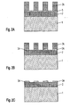
- a carbon hard mask layer 2 is deposited on a substrate 1 to be structured by a plasma-assisted deposition method according to the invention.
- the intermediate layer 5 must have a sufficient etch resistance in the etching of the carbon hard mask layer 2.
- the photoresist layer is then applied to the intermediate layer 5 and patterned so that masked regions 3A remain.
- the structure of the photoresist layer is then first transferred into the intermediate layer 5, so that masked regions 5A of the intermediate layer 5 result below the masked regions 3A of the photoresist layer.
- the SiON layer 5 can be used in a dry etching process with etching gases such as Ar, CHF3, CF4 or the like. be etched for example in a MERIE reactor. Also conceivable are ICP, ECR or other plasma etching reactors.
- the masked photoresist areas 3A are removed in a standard paint shop.
- the carbon hard mask layer 2 is patterned so that masked regions 2A are formed below the masked SiON regions 5A.
- This may preferably be carried out in a dry etching process in a MERIE reactor using O 2 and / or N 2 etching media. This etching can be performed with high selectivity to the masked SiON regions 5A.
- the photoresist can also be removed in-situ, so that the intermediate step of FIG. 2C is saved using the standard varnishing shaver.
- the substrate 1 is patterned by means of the masked carbon hard mask regions 2A, so that structured substrate regions 1A are formed.
Landscapes
- Physics & Mathematics (AREA)
- General Physics & Mathematics (AREA)
- Drying Of Semiconductors (AREA)
- Semiconductor Memories (AREA)
- Crystals, And After-Treatments Of Crystals (AREA)
Claims (12)
- Procédé de production photolithographique de structures dans un substrat (1), dans lequela) on dépose par un procédé de dépôt assisté par plasma une couche (2) de masque dure en carbone sur le substrat (1), le dépôt étant effectué de manière à ce que la couche (2) de masque dure en carbone ait dans au moins une partie de l'épaisseur de couche une dureté comparable à un diamant,b) on structure la couche (2) de masque dure en carbone etc) on transfère la structure de la couche (2) de masque dure en carbone au substrat (1),caractérisé en ce que- on règle dans le stade a) du procédé, lors de la production de la partie d'épaisseur de couche analogue à du diamant, les paramètres lors du dépôt, de façon à rééliminer par des opérations d'attaque ultérieures des parties se formant à la façon du graphite et à laisser subsister des parties se formant en ayant la dureté du diamant.
- Procédé suivant la revendication 1,
caractérisé en ce que- on provoque un bombardement ionique supplémentaire lors du dépôt, notamment par introduction d'Ar et/ou de Ne et/ou- on envoie de l'hydrogène. - Procédé suivant la revendication 1 ou 2,
caractérisé en ce que- dans le stade a) du procédé on utilise comme précurseur de carbone un ou plusieurs des gaz CH4, C2H6, C2H4, C2H2 et C3H6. - Procédé suivant l'une des revendications précédentes,
caractérisé en ce que- au stade a) du procédé on utilise un procédé de dépôt HDP. - Procédé suivant l'une des revendications précédentes,
caractérisé en ce que- lors de la production de la partie d'épaisseur de couche du type du diamant on établit une température du substrat de 200°C à 750°C. - Procédé suivant l'une des revendications précédentes,
caractérisé en ce que- au stade a) du procédé on utilise un procédé de dépôt PECVD. - Procédé suivant l'une des revendications précédentes,
caractérisé en ce que- au stade b) du procédé on dépose sur là couche (2) de masque dure en carbone une couche (3) de réserve photosensible, on la structure photolithographiquement et on transfère la structure dans la couche (2) de masque dure en carbone. - Procédé suivant la revendication 7,
caractérisé en ce que- on introduit une couche (5) intermédiaire entre la couche (2) de masque dure en carbone et la couche (3) de réserve photosensible et- on transfère la structure produite dans la couche (3) de réserve photosensible à la couche (5) intermédiaire et on la transfère ensuite à la couche (2) de masque dure en carbone. - Procédé suivant la revendication 7 ou 8,
caractérisé en ce que- on renforce chimiquement la couche (3) de réserve photosensible après sa structuration. - Procédé suivant l'une des revendications précédentes,
caractérisé en ce que- on forme la couche (2) de masque dure en carbone sous la forme d'une couche à gradient. - Procédé suivant la revendication 10,
caractérisé en ce que- on effectue le stade a) du procédé en modifiant en fonction de la profondeur la composition et/ou la structure de la couche (2) de masque dure en carbone. - Procédé de production de parties d'isolement entre des composants constitués dans un substrat (1), dans lequel- on structure le substrat suivant l'une ou plusieurs des revendications précédentes et- on remplit les parties éliminées d'un matériau isolant.
Applications Claiming Priority (3)
| Application Number | Priority Date | Filing Date | Title |
|---|---|---|---|
| DE10153310 | 2001-10-29 | ||
| DE10153310A DE10153310A1 (de) | 2001-10-29 | 2001-10-29 | Photolithographisches Strukturierungsverfahren mit einer durch ein plasmaunterstützes Abscheideeverfahren hergestellten Kohlenstoff-Hartmaskenschicht diamantartiger Härte |
| PCT/DE2002/004034 WO2003038875A2 (fr) | 2001-10-29 | 2002-10-29 | Procede de structuration photolithographique au moyen d'une couche masque dure, de durete analogue au diamant, obtenue par depot assiste au plasma |
Publications (2)
| Publication Number | Publication Date |
|---|---|
| EP1444724A2 EP1444724A2 (fr) | 2004-08-11 |
| EP1444724B1 true EP1444724B1 (fr) | 2007-01-24 |
Family
ID=7704081
Family Applications (1)
| Application Number | Title | Priority Date | Filing Date |
|---|---|---|---|
| EP02776865A Expired - Lifetime EP1444724B1 (fr) | 2001-10-29 | 2002-10-29 | Procede de structuration photolithographique au moyen d'une couche masque dure, de durete analogue au diamant, obtenue par depot assiste au plasma |
Country Status (6)
| Country | Link |
|---|---|
| US (1) | US7368390B2 (fr) |
| EP (1) | EP1444724B1 (fr) |
| KR (1) | KR100592818B1 (fr) |
| DE (2) | DE10153310A1 (fr) |
| TW (1) | TW583518B (fr) |
| WO (1) | WO2003038875A2 (fr) |
Families Citing this family (43)
| Publication number | Priority date | Publication date | Assignee | Title |
|---|---|---|---|---|
| DE10231533A1 (de) * | 2002-07-11 | 2004-01-29 | Infineon Technologies Ag | Verfahren zur Metallstrukturierung |
| JP4223348B2 (ja) * | 2003-07-31 | 2009-02-12 | Tdk株式会社 | 磁気記録媒体の製造方法及び製造装置 |
| US7132201B2 (en) | 2003-09-12 | 2006-11-07 | Micron Technology, Inc. | Transparent amorphous carbon structure in semiconductor devices |
| US7129180B2 (en) | 2003-09-12 | 2006-10-31 | Micron Technology, Inc. | Masking structure having multiple layers including an amorphous carbon layer |
| DE102004008497A1 (de) | 2004-02-20 | 2005-09-08 | Infineon Technologies Ag | Herstellungsverfahren für eine Halbleiterstruktur in einem Substrat, wobei die Halbleiterstruktur mindestens zwei unterschiedlich zu strukturierende Bereiche aufweist |
| JP2006012332A (ja) * | 2004-06-28 | 2006-01-12 | Tdk Corp | ドライエッチング方法、磁気記録媒体の製造方法及び磁気記録媒体 |
| DE102004031121A1 (de) * | 2004-06-28 | 2006-01-19 | Infineon Technologies Ag | Schichtanordnung und Verfahren zum Herstellen einer Schichtanordnung |
| KR100678460B1 (ko) | 2004-10-12 | 2007-02-02 | 삼성전자주식회사 | 자기정렬 패턴들 사이에 배치된 채널부 홀의 형성방법들 및 이를 이용해서 게이트 패턴들을 갖는 반도체 장치의 형성방법들 |
| US8664124B2 (en) | 2005-10-31 | 2014-03-04 | Novellus Systems, Inc. | Method for etching organic hardmasks |
| US8110493B1 (en) | 2005-12-23 | 2012-02-07 | Novellus Systems, Inc. | Pulsed PECVD method for modulating hydrogen content in hard mask |
| US7981810B1 (en) * | 2006-06-08 | 2011-07-19 | Novellus Systems, Inc. | Methods of depositing highly selective transparent ashable hardmask films |
| US7772126B2 (en) * | 2006-10-19 | 2010-08-10 | Qimonda Ag | Hard mask arrangement, contact arrangement and methods of patterning a substrate and manufacturing a contact arrangement |
| US7538034B2 (en) * | 2006-12-22 | 2009-05-26 | Qimonda Ag | Integrated circuit having a metal element |
| US7981777B1 (en) * | 2007-02-22 | 2011-07-19 | Novellus Systems, Inc. | Methods of depositing stable and hermetic ashable hardmask films |
| US7915166B1 (en) | 2007-02-22 | 2011-03-29 | Novellus Systems, Inc. | Diffusion barrier and etch stop films |
| KR100976647B1 (ko) * | 2007-04-25 | 2010-08-18 | 주식회사 하이닉스반도체 | 반도체 소자의 제조 방법 |
| US8962101B2 (en) | 2007-08-31 | 2015-02-24 | Novellus Systems, Inc. | Methods and apparatus for plasma-based deposition |
| US20090098701A1 (en) * | 2007-10-15 | 2009-04-16 | Jurgen Faul | Method of manufacturing an integrated circuit |
| US7820556B2 (en) * | 2008-06-04 | 2010-10-26 | Novellus Systems, Inc. | Method for purifying acetylene gas for use in semiconductor processes |
| US8435608B1 (en) | 2008-06-27 | 2013-05-07 | Novellus Systems, Inc. | Methods of depositing smooth and conformal ashable hard mask films |
| US7955990B2 (en) * | 2008-12-12 | 2011-06-07 | Novellus Systems, Inc. | Method for improved thickness repeatability of PECVD deposited carbon films |
| US8563414B1 (en) | 2010-04-23 | 2013-10-22 | Novellus Systems, Inc. | Methods for forming conductive carbon films by PECVD |
| CN103137443B (zh) * | 2011-11-25 | 2015-11-25 | 中芯国际集成电路制造(上海)有限公司 | 无定形碳硬掩膜层的形成方法及刻蚀方法 |
| CN103376487B (zh) * | 2012-04-23 | 2016-03-30 | 中芯国际集成电路制造(上海)有限公司 | 光栅的制作方法 |
| SG195494A1 (en) | 2012-05-18 | 2013-12-30 | Novellus Systems Inc | Carbon deposition-etch-ash gap fill process |
| CN103633014B (zh) * | 2012-08-21 | 2018-03-30 | 中国科学院微电子研究所 | 半导体器件制造方法 |
| US9362133B2 (en) | 2012-12-14 | 2016-06-07 | Lam Research Corporation | Method for forming a mask by etching conformal film on patterned ashable hardmask |
| US9304396B2 (en) | 2013-02-25 | 2016-04-05 | Lam Research Corporation | PECVD films for EUV lithography |
| US9320387B2 (en) | 2013-09-30 | 2016-04-26 | Lam Research Corporation | Sulfur doped carbon hard masks |
| US9589799B2 (en) | 2013-09-30 | 2017-03-07 | Lam Research Corporation | High selectivity and low stress carbon hardmask by pulsed low frequency RF power |
| CN103972062A (zh) * | 2014-05-15 | 2014-08-06 | 京东方科技集团股份有限公司 | 一种离子注入的方法 |
| US10410883B2 (en) * | 2016-06-01 | 2019-09-10 | Corning Incorporated | Articles and methods of forming vias in substrates |
| US10794679B2 (en) | 2016-06-29 | 2020-10-06 | Corning Incorporated | Method and system for measuring geometric parameters of through holes |
| US10580725B2 (en) | 2017-05-25 | 2020-03-03 | Corning Incorporated | Articles having vias with geometry attributes and methods for fabricating the same |
| US11078112B2 (en) | 2017-05-25 | 2021-08-03 | Corning Incorporated | Silica-containing substrates with vias having an axially variable sidewall taper and methods for forming the same |
| US12180108B2 (en) | 2017-12-19 | 2024-12-31 | Corning Incorporated | Methods for etching vias in glass-based articles employing positive charge organic molecules |
| US10566207B2 (en) * | 2017-12-27 | 2020-02-18 | Samsung Electronics Co., Ltd. | Semiconductor manufacturing methods for patterning line patterns to have reduced length variation |
| US11554984B2 (en) | 2018-02-22 | 2023-01-17 | Corning Incorporated | Alkali-free borosilicate glasses with low post-HF etch roughness |
| US11145509B2 (en) | 2019-05-24 | 2021-10-12 | Applied Materials, Inc. | Method for forming and patterning a layer and/or substrate |
| CN113891954B (zh) | 2019-05-29 | 2025-09-19 | 朗姆研究公司 | 通过高功率脉冲低频率rf产生的高选择性、低应力、且低氢的类金刚石碳硬掩模 |
| CN114342043A (zh) | 2019-08-30 | 2022-04-12 | 朗姆研究公司 | 低压下的高密度、模量和硬度的非晶碳膜 |
| US11699585B2 (en) * | 2020-10-21 | 2023-07-11 | Applied Materials, Inc. | Methods of forming hardmasks |
| US11501977B1 (en) * | 2021-05-10 | 2022-11-15 | Nanya Technology Corporation | Semiconductor device and manufacturing method thereof |
Family Cites Families (27)
| Publication number | Priority date | Publication date | Assignee | Title |
|---|---|---|---|---|
| DE1904311A1 (de) | 1968-01-31 | 1969-09-04 | Svenska Flaektfabriken Ab | Schleudergeblaese |
| JP3001607B2 (ja) | 1989-04-24 | 2000-01-24 | シーメンス、アクチエンゲゼルシヤフト | 二層法における寸法安定な構造転写方法 |
| EP0395917B1 (fr) | 1989-04-24 | 1997-06-25 | Siemens Aktiengesellschaft | Procédé de structuration photographique |
| EP0539559A1 (fr) | 1991-04-03 | 1993-05-05 | Eastman Kodak Company | MASQUE A HAUTE DUREE POUR L'ATTAQUE A SEC DE GaAs |
| DE4226464B4 (de) | 1992-08-10 | 2005-06-02 | Infineon Technologies Ag | Positivresist |
| US5340696A (en) * | 1993-01-29 | 1994-08-23 | Shipley Company Inc. | Photoresist compositions with copolymer binder having phenolic and nonaromatic cyclic alcohol units where the distribution of the cyclic alcohol concentration is less than 8 mole percent |
| KR100188508B1 (ko) | 1993-03-26 | 1999-06-01 | 세끼사와 다까시 | 비정질탄소막을 사용하는 패턴형성방법과 에칭방법 및 비정질탄소막 형성방법 |
| DE19504434C1 (de) | 1995-02-10 | 1996-05-15 | Siemens Ag | Verfahren zur Herstellung siliziumhaltiger Masken |
| TW302507B (fr) | 1995-02-10 | 1997-04-11 | Siemens Ag | |
| US6153327A (en) * | 1995-03-03 | 2000-11-28 | Southwest Research Institute | Amorphous carbon comprising a catalyst |
| JPH1082390A (ja) * | 1996-07-18 | 1998-03-31 | Sanyo Electric Co Ltd | 摺動部材、圧縮機及び回転圧縮機 |
| GB9616043D0 (en) * | 1996-07-31 | 1996-09-11 | De Beers Ind Diamond | Diamond |
| JP3228183B2 (ja) * | 1996-12-02 | 2001-11-12 | 日本電気株式会社 | 絶縁膜ならびにその絶縁膜を有する半導体装置とその製造方法 |
| GB9703571D0 (en) * | 1997-02-20 | 1997-04-09 | De Beers Ind Diamond | Diamond-containing body |
| US5981398A (en) * | 1998-04-10 | 1999-11-09 | Taiwan Semiconductor Manufacturing Company, Ltd. | Hard mask method for forming chlorine containing plasma etched layer |
| US6030541A (en) * | 1998-06-19 | 2000-02-29 | International Business Machines Corporation | Process for defining a pattern using an anti-reflective coating and structure therefor |
| JP3259704B2 (ja) * | 1998-12-30 | 2002-02-25 | 日本電気株式会社 | 半導体装置の製造方法 |
| DE19941148B4 (de) | 1999-08-30 | 2006-08-10 | Infineon Technologies Ag | Speicher mit Grabenkondensator und Auswahltransistor und Verfahren zu seiner Herstellung |
| DE19944012B4 (de) | 1999-09-14 | 2007-07-19 | Infineon Technologies Ag | Grabenkondensator mit Kondensatorelektroden und entsprechendes Herstellungsverfahren |
| DE19945425A1 (de) | 1999-09-22 | 2001-04-19 | Infineon Technologies Ag | Verfahren zum Strukturieren einer Metallschicht in der Halbleiterfertigung |
| DE19958904C2 (de) | 1999-12-07 | 2002-01-24 | Infineon Technologies Ag | Verfahren zur Herstellung einer Hartmaske auf einem Substrat |
| US6573030B1 (en) * | 2000-02-17 | 2003-06-03 | Applied Materials, Inc. | Method for depositing an amorphous carbon layer |
| EP1290251B8 (fr) * | 2000-06-15 | 2006-02-01 | Element Six (PTY) Ltd | Couche de diamant monocristallin epaisse, procede de fabrication, et pierres precieuses produites a partir de cette couche |
| US6633497B2 (en) | 2001-06-22 | 2003-10-14 | Hewlett-Packard Development Company, L.P. | Resistive cross point array of short-tolerant memory cells |
| GB0130005D0 (en) * | 2001-12-14 | 2002-02-06 | Diamanx Products Ltd | Boron doped diamond |
| US6673684B1 (en) * | 2002-07-31 | 2004-01-06 | Advanced Micro Devices, Inc. | Use of diamond as a hard mask material |
| US6884733B1 (en) * | 2002-08-08 | 2005-04-26 | Advanced Micro Devices, Inc. | Use of amorphous carbon hard mask for gate patterning to eliminate requirement of poly re-oxidation |
-
2001
- 2001-10-29 DE DE10153310A patent/DE10153310A1/de not_active Ceased
-
2002
- 2002-10-23 TW TW091124512A patent/TW583518B/zh not_active IP Right Cessation
- 2002-10-29 EP EP02776865A patent/EP1444724B1/fr not_active Expired - Lifetime
- 2002-10-29 DE DE50209381T patent/DE50209381D1/de not_active Expired - Fee Related
- 2002-10-29 US US10/494,063 patent/US7368390B2/en not_active Expired - Lifetime
- 2002-10-29 KR KR1020047006329A patent/KR100592818B1/ko not_active Expired - Fee Related
- 2002-10-29 WO PCT/DE2002/004034 patent/WO2003038875A2/fr not_active Ceased
Also Published As
| Publication number | Publication date |
|---|---|
| KR20040051622A (ko) | 2004-06-18 |
| EP1444724A2 (fr) | 2004-08-11 |
| KR100592818B1 (ko) | 2006-06-26 |
| US20050112506A1 (en) | 2005-05-26 |
| WO2003038875A2 (fr) | 2003-05-08 |
| DE50209381D1 (de) | 2007-03-15 |
| US7368390B2 (en) | 2008-05-06 |
| WO2003038875A3 (fr) | 2003-11-06 |
| DE10153310A1 (de) | 2003-05-22 |
| TW583518B (en) | 2004-04-11 |
Similar Documents
| Publication | Publication Date | Title |
|---|---|---|
| EP1444724B1 (fr) | Procede de structuration photolithographique au moyen d'une couche masque dure, de durete analogue au diamant, obtenue par depot assiste au plasma | |
| DE102017128235B4 (de) | Strukturierungsverfahren für ein halbleiterbauelement und daraus resultierende strukturen | |
| DE69025300T2 (de) | Integrierte Schaltung mit einer planarisierten dielektrischen Schicht | |
| DE69412945T2 (de) | Chemisch-mechanische Planarisierung von flachen Rillen auf Halbleitersubstraten | |
| DE69232648T2 (de) | Verfahren zur Herstellung einer Grabenisolation mittels eines Polierschritts und Herstellungsverfahren für eine Halbleitervorrichtung | |
| DE102008007671B4 (de) | Verfahren zur Bildung feiner Strukturen eines Halbleiterbauelements | |
| DE10339989B4 (de) | Verfahren zur Herstellung eines konformen Abstandselements benachbart zu einer Gateelektrodenstruktur | |
| DE112012005734B4 (de) | Lithographieprozess und Lithographische Struktur mit doppelter Hartmaske | |
| DE3856022T2 (de) | Selektives Ätzen dünner Schichten | |
| DE10030308B4 (de) | Verfahren zur Herstellung eines Kontaktstifts und eines Halbleiterbauelementes | |
| DE102016100766A1 (de) | Strukturierung von durchkontaktierungen durch mehrfachfotolithografie und mehrfachätzung | |
| DE10127622B4 (de) | Verfahren zur Herstellung eines mit HDPCVD-Oxid gefüllten Isolationsgrabens | |
| DE19929239A1 (de) | Verfahren zur Herstellung von Halbleitern | |
| DE102010064289A1 (de) | Größenreduzierung von Kontaktelementen und Kontaktdurchführungen in einem Halbleiterbauelement durch Einbau eines zusätzlichen Abschrägungsmaterials | |
| DE69130787T2 (de) | Ätzverfahren für eine leitende Doppelschicht-Struktur | |
| EP0338102B1 (fr) | Procédé de fabrication de circuits intégrés à semi-conducteurs comportant des transistors à effet de champ ayant des canaux submicroniques | |
| DE102021114103A1 (de) | Metallische hartmasken zum reduzieren der leitungskrümmung | |
| DE112006000811B4 (de) | Ätzprozess für CD-Reduzierung eines ARC-Materials | |
| DE69324524T2 (de) | Verfahren zur Herstellung eines Halbleiter-Speicherbauteils | |
| DE10339988B4 (de) | Verfahren zur Herstellung einer antireflektierenden Schicht | |
| DE10029036C1 (de) | Verfahren zur Erhöhung der Trenchkapazität | |
| DE10226603A1 (de) | Verfahren zum Strukturieren einer Siliziumschicht sowie dessen Verwendung zur Herstellung einer integrierten Halbleiterschaltung | |
| DE102004029516B3 (de) | Herstellungsverfahren für eine Schattenmaske in einem Graben einer mikroelektronischen oder mikromechanischen Struktur sowie Verwendung derselben | |
| DE102009046259B4 (de) | Stärkere Haftung eines PECVD-Kohlenstoffs auf dielektrischen Materialien durch Vorsehen einer Haftungsgrenzfläche | |
| DE102004036753A1 (de) | Stickstofffreie ARC-Deckschicht und Verfahren zur Herstellung derselben |
Legal Events
| Date | Code | Title | Description |
|---|---|---|---|
| PUAI | Public reference made under article 153(3) epc to a published international application that has entered the european phase |
Free format text: ORIGINAL CODE: 0009012 |
|
| 17P | Request for examination filed |
Effective date: 20040422 |
|
| AK | Designated contracting states |
Kind code of ref document: A2 Designated state(s): DE FR GB IE IT |
|
| GRAP | Despatch of communication of intention to grant a patent |
Free format text: ORIGINAL CODE: EPIDOSNIGR1 |
|
| GRAS | Grant fee paid |
Free format text: ORIGINAL CODE: EPIDOSNIGR3 |
|
| GRAA | (expected) grant |
Free format text: ORIGINAL CODE: 0009210 |
|
| AK | Designated contracting states |
Kind code of ref document: B1 Designated state(s): DE |
|
| REF | Corresponds to: |
Ref document number: 50209381 Country of ref document: DE Date of ref document: 20070315 Kind code of ref document: P |
|
| PLBE | No opposition filed within time limit |
Free format text: ORIGINAL CODE: 0009261 |
|
| STAA | Information on the status of an ep patent application or granted ep patent |
Free format text: STATUS: NO OPPOSITION FILED WITHIN TIME LIMIT |
|
| 26N | No opposition filed |
Effective date: 20071025 |
|
| PGFP | Annual fee paid to national office [announced via postgrant information from national office to epo] |
Ref country code: DE Payment date: 20071211 Year of fee payment: 6 |
|
| PG25 | Lapsed in a contracting state [announced via postgrant information from national office to epo] |
Ref country code: DE Free format text: LAPSE BECAUSE OF NON-PAYMENT OF DUE FEES Effective date: 20090501 |