EP1445862B1 - Circuit de commande de transistor et de registre à décalage - Google Patents
Circuit de commande de transistor et de registre à décalage Download PDFInfo
- Publication number
- EP1445862B1 EP1445862B1 EP04002418A EP04002418A EP1445862B1 EP 1445862 B1 EP1445862 B1 EP 1445862B1 EP 04002418 A EP04002418 A EP 04002418A EP 04002418 A EP04002418 A EP 04002418A EP 1445862 B1 EP1445862 B1 EP 1445862B1
- Authority
- EP
- European Patent Office
- Prior art keywords
- pull
- transistor
- signal
- vgs
- control signal
- Prior art date
- Legal status (The legal status is an assumption and is not a legal conclusion. Google has not performed a legal analysis and makes no representation as to the accuracy of the status listed.)
- Expired - Lifetime
Links
Images



Classifications
-
- G—PHYSICS
- G09—EDUCATION; CRYPTOGRAPHY; DISPLAY; ADVERTISING; SEALS
- G09G—ARRANGEMENTS OR CIRCUITS FOR CONTROL OF INDICATING DEVICES USING STATIC MEANS TO PRESENT VARIABLE INFORMATION
- G09G3/00—Control arrangements or circuits, of interest only in connection with visual indicators other than cathode-ray tubes
- G09G3/20—Control arrangements or circuits, of interest only in connection with visual indicators other than cathode-ray tubes for presentation of an assembly of a number of characters, e.g. a page, by composing the assembly by combination of individual elements arranged in a matrix no fixed position being assigned to or needed to be assigned to the individual characters or partial characters
-
- G—PHYSICS
- G09—EDUCATION; CRYPTOGRAPHY; DISPLAY; ADVERTISING; SEALS
- G09G—ARRANGEMENTS OR CIRCUITS FOR CONTROL OF INDICATING DEVICES USING STATIC MEANS TO PRESENT VARIABLE INFORMATION
- G09G3/00—Control arrangements or circuits, of interest only in connection with visual indicators other than cathode-ray tubes
- G09G3/20—Control arrangements or circuits, of interest only in connection with visual indicators other than cathode-ray tubes for presentation of an assembly of a number of characters, e.g. a page, by composing the assembly by combination of individual elements arranged in a matrix no fixed position being assigned to or needed to be assigned to the individual characters or partial characters
- G09G3/34—Control arrangements or circuits, of interest only in connection with visual indicators other than cathode-ray tubes for presentation of an assembly of a number of characters, e.g. a page, by composing the assembly by combination of individual elements arranged in a matrix no fixed position being assigned to or needed to be assigned to the individual characters or partial characters by control of light from an independent source
- G09G3/36—Control arrangements or circuits, of interest only in connection with visual indicators other than cathode-ray tubes for presentation of an assembly of a number of characters, e.g. a page, by composing the assembly by combination of individual elements arranged in a matrix no fixed position being assigned to or needed to be assigned to the individual characters or partial characters by control of light from an independent source using liquid crystals
-
- G—PHYSICS
- G11—INFORMATION STORAGE
- G11C—STATIC STORES
- G11C19/00—Digital stores in which the information is moved stepwise, e.g. shift registers
- G11C19/28—Digital stores in which the information is moved stepwise, e.g. shift registers using semiconductor elements
-
- G—PHYSICS
- G09—EDUCATION; CRYPTOGRAPHY; DISPLAY; ADVERTISING; SEALS
- G09G—ARRANGEMENTS OR CIRCUITS FOR CONTROL OF INDICATING DEVICES USING STATIC MEANS TO PRESENT VARIABLE INFORMATION
- G09G2310/00—Command of the display device
- G09G2310/02—Addressing, scanning or driving the display screen or processing steps related thereto
- G09G2310/0264—Details of driving circuits
- G09G2310/0267—Details of drivers for scan electrodes, other than drivers for liquid crystal, plasma or OLED displays
-
- G—PHYSICS
- G09—EDUCATION; CRYPTOGRAPHY; DISPLAY; ADVERTISING; SEALS
- G09G—ARRANGEMENTS OR CIRCUITS FOR CONTROL OF INDICATING DEVICES USING STATIC MEANS TO PRESENT VARIABLE INFORMATION
- G09G2310/00—Command of the display device
- G09G2310/02—Addressing, scanning or driving the display screen or processing steps related thereto
- G09G2310/0264—Details of driving circuits
- G09G2310/0286—Details of a shift registers arranged for use in a driving circuit
Definitions
- the present invention relates to display devices for displaying images, and more particularly, to a shift register for the display devices and a method of driving a transistor in the shift register.
- liquid crystal display devices are equipped with a gate driver integrated circuit which is mounted on a liquid crystal display panel by means of a tape carrier package (TCP) or a chip-on-glass (COG) method.
- the liquid crystal display devices equipped with a gate driver integrated circuit have disadvantages such as high the manufacturing cost and structural hindrance in designing a liquid crystal display device.
- the liquid crystal display devices have been developed to employ a "gate-IC-less" structure, in which no such gate driver integrated circuit is mounted on a liquid crystal display panel.
- a driving circuit using amorphous-silicon thin film transistors (a-Si TFTs) is employed to perform the substantially same function as performed by the gate driver integrated circuit.
- Examples of a shift register circuit for display devices which includes amorphous-silicon thin film transistors, are disclosed in the U.S. Patent No. 5,517,542 and the U.S. Laid Open Publication No. 2002-0149318 .
- the shift register circuit disclosed in the U.S. Laid Open Publication No. 2002-0149318 includes seven amorphous-silicon thin film transistors in its each stage.
- US 2002/0044625 A1 discloses shift registers, which substantially correspond to the shift registers as described with reference to the following FIGS. 1 to 4 .
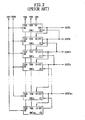
- FIG. 1 is a circuit diagram illustrating a stage of a conventional shift register such as one disclosed in the U.S. Laid Open Publication No. 2002-0149318
- FIG. 2 is a block diagram illustrating a shift register having multiple stages.
- the shift register replaces the gate driver integrated circuit.
- the shift register is integrated in a thin film transistor liquid crystal display panel to perform the same operation as the gate driver integrated circuit does.
- each of the stages in the shift register includes a pull-up part 110, a pull-down part 120, a pull-up driver 130 and a pull-down driver 140.
- the present stage receives a gate line driving signal GOUT N-1 (or scan line driving signal) from a previous stage, and the present stage generates a gate line driving signal GOUT N .
- the present stage is the first stage of the shift register
- the first stage receives a start signal STV generated from a timing controller (not shown), and the first stage generates a first gate line driving signal GOUT 1 .
- the second stage receives the first gate line driving signal GOUT 1 generated from the first stage, and the second stage generates a second gate line driving signal GOUT 2 .
- the present stage receives an (N-1)th gate line driving signal GOUT N-1 generated from an (N-1)th stage, and the Nth stage generates an Nth gate line driving signal GOUT N .
- the shift register having the N stages sequentially generates the gate line driving signals GOUT 1 , GOUT 2 , ..., GOUT N .
- the shift register also receives clock signals CKV and CKVB and voltage signals externally provided, and each stage of the shift register has multiple input terminals to receive those signals as well as other control signals and an output terminal to generate the corresponding gate line driving signal.
- clock signals CKV and CKVB and voltage signals externally provided, and each stage of the shift register has multiple input terminals to receive those signals as well as other control signals and an output terminal to generate the corresponding gate line driving signal.
- the first stage SRC 1 receives the start signal STV generated from the timing controller (not shown), a gate turn-on voltage VON, a gate turn-off voltage VOFF, and a first clock signal CKV.
- the first stage SRC1 generates the first gate line driving signal GOUT 1 for selecting a first gate line.
- the first gate line driving signal GOUT 1 is provided to the first gate line and an input terminal (IN) of the second stage SRC2.
- the second stage SRC 2 receives the first gate line driving signal GOUT 1 generated from the first stage SRC1, the gate turn-on voltage VON, the gate turn-off voltage VOFF, and a second clock signal CKVB.
- the second stage SRC2 generates the second gate line driving signal GOUT 2 for selecting a second gate line.
- the second gate line driving signal GOUT 2 is provided to the second gate line and an input terminal (IN) of the third stage SRC 3 .
- the Nth stage SRC N receives the (N-1)th gate line driving signal GOUT N-1 generated form the (N-1)th stage, the gate turn-on voltage VON, the gate turn-off voltage VOFF, and the second clock signal CKVB.
- the Nth stage SRC N generates the Nth gate line driving signal GOUT N for selecting an Nth gate line.
- the Nth gate line driving signal GOUT N is provided to the Nth gate line and an input terminal (IN) of the (N+1)th stage SRC N+1 .
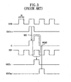
- FIG. 3 is a timing diagram for describing the operation of the conventional shift register in FIGS. 1 and 2 .
- the shift register receives the first clock signal CKV and the second clock signal CKVB and sequentially outputs the gate line driving signals to the gate lines formed on a TFT substrate.
- the second clock signal CKVB has a 180° phase difference with respect to the first clock signal CKV.
- the amplitudes of the first and second clock signals CKV, CKVB are in a range from about -8 volt to about 24 volt.
- the amplitude of the output signal of the timing controller (not shown) is in a range from about 0 volt to about 3 volt.
- the output signal of the timing controller (not shown) is amplified so that the first and second clock signals CKV, CKVB have the amplitudes in the range from about -8 volt to about 24 volt.
- the NMOS transistor Q1 of the pull-up part 110 includes amorphous-silicon
- the NMOS transistor Q1 has a relatively large transistor size. This is because, in order to drive the liquid crystal display device having a large screen size, a large amplitude of voltage (for example, from -14V to 20V) should be applied to the NMOS transistor Q1 due to the very small electron mobility of the amorphous-silicon of the NMOS transistor Q1.
- parasitic capacitance of a gate line has a value from about 250pF to about 300pF.
- a channel width of the amorphous-silicon thin film transistor should be about 5500 ⁇ m when a channel length of the amorphous-silicon thin film transistor is about 4 ⁇ m.
- the parasitic capacitance between a gate electrode and a drain electrode of the NMOS amorphous-silicon thin film transistor Q1 increases.
- the value of the parasitic capacitance is about 3pF. This value causes a malfunction of the gate driver circuit employing the NMOS amorphous-silicon thin film transistor. The malfunction occurs as follows.
- the parasitic capacitor is electrically connected with a terminal to which the clock signal CKV or CKVB having a large amplitude of voltage (for example, from about -14V to about 20V) is applied, and the parasitic capacitor (or coupling capacitor) is electrically connected between the drain and gate electrodes of the NMOS amorphous-silicon thin film transistor Q1 to apply undesired voltage signal to the gate electrode of the NMOS amorphous-silicon thin film transistor Q1.
- the clock signal CKV or CKVB having the amplitude between about -14V and about 20V is applied to the gate electrode of the NMOS amorphous-silicon thin film transistor Q1.
- the voltage level of the gate electrode of the NMOS transistor Q1 becomes in the range from about -14V to about 20V, and the output signal equals to '20V (maximum value) - Vth (the threshold voltage of the NMOS amorphous-silicon transistor Q1)'. Applying such output signal to the gate line of the liquid crystal display panel causes abnormal display of images.
- a hold transistor Q5 is employed.
- the hold transistor Q5 is an amorphous-silicon thin film transistor.
- a pull-down thin film transistor Q2 performing a pull down function is employed to maintain the scan signal at the gate turn-off voltage level VOFF during most of the period after the pull-up transistor Q1 operates.
- the hold transistor Q5 receives a DC voltage signal proportional to the gate turn-on voltage VON (DC voltage signal) through the gate electrode of the hold transistor Q5 during the period except for the time period of 'one vertical synchronization period - two horizontal synchronization periods'.
- the pull-down transistor Q2 receives a DC voltage signal proportional to the gate turn-on voltage VON (DC voltage signal) through the gate electrode of the pull-down transistor Q2 during the period except for the time period of 'one vertical synchronization period - two horizontal synchronization period'.
- one vertical synchronization period denotes a time interval between two consecutive frames.
- one vertical synchronization period is referred to as the time interval between the vertical synchronization signals (Vsync).
- the vertical synchronization signal (Vsync) indicates the point of time where a frame begins.
- One horizontal synchronization period denotes a time interval between two consecutive scan lines. Namely, one horizontal synchronization period is referred to as the time interval between the horizontal synchronization signals (Hsync).
- the horizontal synchronization signal (Hsync) indicates the point of time where a scan line of a frame begins.
- the pull-down transistor Q2 and the hold transistor Q5 may be deteriorated since the DC voltage signal is applied to the gate electrodes of the pull-down transistor Q2 and the hold transistor Q5 for most of the operation period.
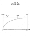
- FIG, 4 is a graph showing the variation of the threshold voltage of an a-Si TFT when a DC gate-source voltage is applied to the gate electrode of the a-Si TFT.
- the threshold voltage (Vth) of the a-Si transistor is increased due to the deterioration of the a-Si transistor.
- the a-Si transistor is not turned on even when a normal gate-source voltage Vgs is applied thereto.
- the shift register has a plurality of stages each providing a gate line driving signal to a corresponding gate line of a display panel, and the stages each include a pull-up part to generate a current gate line driving signal having a first state in response to a first control signal and a clock signal, a pull-down part to generate the current gate line driving signal having a second state in response to a second control signal, a pull-up driver to generate the first control signal to control the pull-up part in response to a an adjacent gate line driving signal provided from an adjacent previous stage, and an input voltage signal externally provided, and a pull-down driver to generate the second control signal to control the pull-down part.
- the second control signal is a pulse signal swing ing s between a maximum voltage level and a minimum voltage levels in response to the input voltage signal swinging between a maximum voltage level and a minimum voltage levels.
- the pull-down driver includes an inverter to generate a third control signal in response to the input voltage signal and the first control signal from the pull-up driver, and a deterioration compensation part to generate the second control signal in response to the input voltage signal, the first control signal from the pull-up driver, and the third control signal from the inverter.
- FIG. 5A is an equivalent circuit diagram of the an a-Si TFT according to the present invention
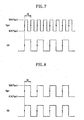
- FIG. 5B is a graph showing a waveform of a gate-source voltage signal applied to the a-Si TFT.
- a drain voltage (Vd) is applied to a drain electrode (D) of the a-Si TFT
- a source voltage (Vs) is applied to a source electrode (S) of the a-Si TFT
- a gate voltage (Vg) is applied to a gate electrode (G) of the a-Si TFT.
- the a-Si TFT When the gate voltage (Vg) is applied to the gate electrode (G) of the a-Si TFT, the a-Si TFT becomes turned on or off depending on the gate-source voltage (Vgs), a voltage difference between the gate voltage (Vg) and the source voltage (Vs). For example, when the gate-source voltage (Vgs) applied to the gate electrode (G) of the a-Si TFT is lower than the threshold voltage of the a-Si TFT, the a-Si TFT is turned off. When the gate-source voltage (Vgs) applied to the gate electrode (G) of the a-Si TFT is higher than the threshold voltage of the a-Si TFT, the a-Si TFT is turned on.
- a gate-source voltage (Vgs_ac) signal as shown in FIG. 5B is established between the gate electrode (G) and the source electrode (S) of the a-Si TFT.
- the gate-source voltage (Vgs_ac) signal is a pulse signal swinging between a maximum voltage level Max(Vgs) and a minimum voltage level Min(Vgs) at a predetermined period.
- the gate voltage (Vg) applied to the gate electrode (G) of the a-Si TFT is also a pulse signal swinging between a maximum voltage level and a minimum voltage level at a predetermined period, so that the gate-source voltage (Vgs_ac) is established between the gate and source electrodes of the a-Si TFT.
- the a-Si transistor Since the gate-source voltage (Vgs_ac) between the gate electrode (G) and the source electrode (S) of the a-Si TFT swings between the maximum voltage level Max(Vgs) and the minimum voltage level Min(Vgs) at the predetermined period, the a-Si transistor is turned on even when a normal threshold voltage of the a-Si TFT is increased by ' ⁇ Vth' due to the deterioration of the a-Si transistor. As shown in FIG.
- a pulse-type gate voltage (Vg) signal swinging between a maximum voltage and a minimum voltage at the predetermined period is applied to the gate electrode (G) of the a-Si TFT in a shift register.
- FIG. 6 is a circuit diagram showing a stage of a shift register according to an exemplary embodiment of the present invention.
- the shift register has multiple stages each having the substantially same configuration as shown in FIG. 6 .
- the stage of the shift register includes a pull-up part 210, a pull-down part 220, a pull-up driver 230, and a pull-down driver 240.
- the current stage receives a gate line driving signal GOUT N-1 (or a scan line driving signal) from a previous stage, and generates a current gate line driving signal GOUT N .
- the first stage receives a start signal generated from a timing controller (not shown), and generates a first gate line driving signal GOUT 1 .
- the second stage receives the first gate line driving signal GOUT 1 generated from the first stage and generates a second gate line driving signal GOUT 2 .
- the Nth stage receives an (N-1)th gate line driving signal GOUT N-1 generated from the (N-1)th stage and generates the Nth gate line driving signal GOUT N .
- the stages of the shift register are arranged in such a manner as to generate the gate line driving signals in sequence, and the shift register is integrated in a thin film transistor liquid crystal display panel.
- the pull-up part 210 includes a NMOS pull-up transistor Q1.
- a clock terminal (CKV terminal or CKVB terminal) is connected to the drain electrode of the NMOS pull-up transistor Q1, a gate electrode of the NMOS pull-up transistor Q1 is connected to a first node N1, and an output terminal OUT is connected to a source electrode of the NMOS pull-up transistor Q1.
- the pull-down part 220 includes a NMOS pull-down transistor Q2.
- the output terminal OUT is connected to a drain electrode of the NMOS pull-down transistor Q2, a gate electrode of the NMOS pull-down transistor Q2 is connected to the pull-down driver 240, and a source electrode of the NMOS pull-down transistor Q2 is connected to a gate turn-off voltage (VOFF) terminal.
- VOFF gate turn-off voltage
- the pull-up driver 230 includes a capacitor C and NMOS transistors (Q3, Q4, Q5). Particularly, the capacitor C is connected between the first node N1 and the output terminal OUT.
- a drain electrode of the NMOS transistor Q3 is connected to a gate turn-on voltage (VON) terminal, a gate electrode of the NMOS transistor Q3 is connected to an output terminal OUT N-1 of a previous stage, and a source electrode of the NMOS transistor Q3 is connected to the first node N1.
- VON gate turn-on voltage
- the previous stage providing the previous gate line driving signal GOUT N-1 is a stage right next to the current stage or one of the stages preceding the current stage.
- the NMOS transistor Q4 of the pull-up driver 230 has a drain electrode connected to the first node N1, a gate electrode connected to a control terminal CT, and a source electrode connected to the gate turn-off voltage (VOFF) terminal.
- the gate turn-off voltage (VOFF) is, for example, a power voltage signal for the shift register.
- the control terminal CT receives a gate line driving signal from a following stage. It is noted that the following stage providing its output signal (i.e., the gate line driving signal) to the current stage is a stage right next to current stage or one of the stages following the current stage.
- a drain electrode of the NMOS transistor Q5 is connected to the first node N1, a gate electrode of the NMOS transistor Q4 is connected to the gate electrode of the pull-down NMOS transistor Q2, and a source electrode of the NMOS transistor Q5 is connected to the gate turn-off voltage (VOFF) terminal.
- the pull-down driver 240 includes an inverter 242 and a deterioration compensation part 244.
- the inverter 242 includes two NMOS transistors Q6 and Q7, and the deterioration compensation section 244 includes two NMOS transistors MA and MB.
- gate and drain electrodes of the NMOS transistor Q6 are commonly connected to the gate turn-on voltage (VON) terminal.
- a drain of the NMOS transistor Q7 is connected to the source of the NMOS transistor Q6, a gate of the NMOS transistor Q7 is connected to the source of the NMOS transistor Q3 via the first node N1, and a source electrode of the NMOS transistor Q7 is connected to the gate turn-off voltage (VOFF) terminal.
- a drain of the NMOS transistor MA is connected to the gate turn-on voltage (VON) terminal, a gate of the NMOS transistor MA is connected to the source electrode of the NMOS transistor Q6 and the drain electrode of the NMOS transistor Q7.
- a source electrode of the NMOS transistor MA is connected to a third node N3 that is connected to the gate electrodes of the pull-down transistor Q2 and the hold transistor Q5.
- a drain of the NMOS transistor MB is connected to the third node N3.
- a gate of the NMOS transistor MB is connected to the first node N1, and a source electrode of the NMOS transistor MB is connected to the gate turn-off voltage (VOFF) terminal.
- the deterioration compensation section 244 provides a pulse-type voltage signal to the gate electrodes of the pull-down transistor Q2 and the hold transistor Q5. The pulse-type voltage signal swings between predetermined maximum and minimum voltage values.
- V MA_Gate Max VON - Vth Q ⁇ 6
- 'V(MA_Gate)' denotes the voltage applied to the gate of the NMOS transistor MA
- 'Max(VON)' denotes the maximum voltage of the gate turn-on voltage signal VON
- 'Vth(Q6)' denotes the threshold voltage of the NMOS transistor Q6.
- V N ⁇ 3 V MA_Gate - Vth MA
- 'V(N3)' denotes the voltage at the third note N3
- 'Vth(MA)' denotes the threshold voltage of the NMOS transistor MA.
- the NMOS transistor Q6 When a minimum voltage of the turn-on voltage signal is applied to the gate turn-on voltage VON terminal, the NMOS transistor Q6 is turned off and the voltage applied to the gate capacitor of the NMOS transistor MA decreases due to the coupling effect between the voltage level of the drain electrode of the NMOS transistor MA and the voltage level of the third node N3. Since the minimum voltage of the turn-on voltage signal is smaller than the voltage at the third node N3, the third node N3 is discharged in accordance with the condition such as 'V(MA_Gate) > Min(VON) + Vth(MA)' (here, 'Min(VON)' denotes the minimum voltage of the turn-on voltage signal VON).
- the NMOS transistor MA is a symmetric transistor
- half of the total parasitic capacitance of the NMOS transistor MA is substantially equal to the parasitic capacitance Cgs between the gate and source electrodes of the NMOS transistor MA and also to the parasitic capacitance Cgd between the gate and drain electrodes of the NMOS transistor MA.
- the third node N3 has a voltage of the following Expression 4.
- V N ⁇ 3 - Min VON + 3 ⁇ Vth MA This is because the gate electrode of the NMOS transistor MA is discharged until the voltage V(MA_Gate) of the gate electrode of the NMOS transistor MA reaches the voltage value of 'the minimum turn-on voltage signal Min(VON) + the threshold voltage Vth(MA) of the NMOS transistor MA'.
- the voltage V(N3) at the third node N3 is applied to the gate electrodes of the pull-down transistor Q2 and the hold transistor Q5.
- the pull-down a-Si transistor Q2 is turned on when the voltage level of the clock signal (CKV or CKVB) changes from a low level to a high level during the period of 'one vertical synchronization period - one horizontal synchronization period'. Also, the pull-down a-Si transistor Q5 is turned on when the voltage level of the clock signal (CKV or CKVB) changes from a low level to a high level during the period of 'one vertical synchronization period - tow horizontal synchronization periods'.
- the maximum value of the gate-source voltage Vgs of the pull-down transistor Q2 (or the hold transistor Q5) should be larger than the sum of the normal threshold voltage Vtho of the pull-down transistor Q2 (or the hold transistor Q5) and the threshold voltage difference ⁇ Vth.
- the threshold voltage difference ⁇ Vth denotes the voltage difference between the normal threshold voltage Vtho and the threshold voltage of a deteriorated pull-down transistor Q2 (or the hold transistor Q5). This is presented by the following Expression 5.
- 'Max(Vgs)' denotes the maximum value of the gate-source voltage Vgs of the pull-down transistor Q2 (or the hold transistor Q5). Since the pull-down transistor Q2 or the hold transistor Q5 should be maintained in a turn-on state even when the threshold voltage difference ⁇ Vth reaches the value of '(Max(Vgs)+Min(Vgs))/2', the following Expression 6 should be satisfied.
- Max Vgs - Min Vgs / 2 > Vtho Therefore , Max Vgs - Min Vgs / 2 ⁇ Vtho
- Max(Vgs) of the gate-source voltage Vgs and the minimum value Min(Vgs) of the gate-source voltage Vgs are presented by the following Expressions 7 and 8, respectively.
- Max Vgs Max VON - Vth Q ⁇ 6 - Vth MA - VOFF
- Min Vgs Min VON + 3 ⁇ Vth MA - VOFF
- the pull-down transistor Q2 when the amplitude of the gate turn-on voltage VON is larger than seven times that of the normal threshold voltage Vtho of the pull-down transistor Q2 (or the hold transistor Q5), the pull-down transistor Q2 (or the hold transistor Q5) normally operates even when the pull-down transistor Q2 (or the hold transistor Q5) is deteriorated.
- FIG. 7 is a timing diagram showing a waveform of the gate-source voltage signal applied to the a-Si TFT, i.e., the pull-down transistor Q2 or the hold transistor Q5 in this embodiment.
- the pulse signal swings between a maximum voltage level MAX(Vgs) and a minimum voltage level MIN(Vgs) and has a predetermined period substantially equal to the half of a period of the clock CK.
- the rising edge of the gate-source voltage signal is synchronized with the rising edge of the clock signal CK, and the voltage level of the gate-source voltage signal changes from the maximum voltage level MAX(Vgs) to the minimum voltage level MIN(Vgs) at the half (1 ⁇ 2H) of its period (H). Then, the voltage level of the gate-source voltage signal changes from the minimum voltage level MIN(Vgs) to the maximum voltage level MAX(Vgs) when the voltage level of the clock signal CK changes from a high level to a low level.
- the gate-source voltage Vgs has the rising edge synchronized with the transition of the clock CK.
- the gate-source voltage Vgs has the maximum value when the voltage level of the clock CK changes from the low level to the high level or changes from the high level to the low level.
- the gate-source voltage Vgs applied to the pull-down transistor Q2 (or the hold transistor Q5) has the amplitude larger than two times that of the normal threshold voltage Vtho of the pull-down transistor Q2 (or the hold transistor Q5).
- FIG. 8 is a timing diagram showing a waveform of another example of the gate-source voltage signal applied to the a-Si TFT.
- the gate-source voltage signal swings between the maximum voltage level MAX(Vgs) and the minimum voltage level MIN(Vgs) has a predetermined period substantially equal to the period of the clock CK.
- the gate-source voltage signal is synchronized with the clock CK, such that the rising edge of the gate-source voltage signal is synchronized with the rising edge of the clock CK and the falling edge of the gate-source voltage signal is synchronized with the falling edge of the clock CK.
- the gate-source voltage signal of this example also has the amplitude larger than two times that of the normal threshold voltage Vtho of the pull-down transistor Q2 (or the hold transistor Q5).
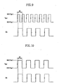
- FIGS. 9 and 10 are timing diagrams showing further other examples of the gate-source voltage applied to the a-Si TFT. As shown in FIGS. 9 and 10 , the phase of the gate-source voltage signal leads that of the clock CK. In FIG. 9 , the phase of the rising edge of the gate-source voltage signal leads the phase of the transition of the clock CK. In FIG. 10 , the phase of the rising edge of the gate-source voltage signal leads the phase of the rising edge of the clock CK.
Landscapes
- Engineering & Computer Science (AREA)
- Physics & Mathematics (AREA)
- Computer Hardware Design (AREA)
- General Physics & Mathematics (AREA)
- Theoretical Computer Science (AREA)
- Chemical & Material Sciences (AREA)
- Crystallography & Structural Chemistry (AREA)
- Control Of Indicators Other Than Cathode Ray Tubes (AREA)
- Shift Register Type Memory (AREA)
- Liquid Crystal Display Device Control (AREA)
- Electronic Switches (AREA)
- Liquid Crystal (AREA)
Claims (16)
- Registre à décalage possédant une pluralité d'étages fournissant chacun un signal d'excitation de ligne de grille à une ligne de grille correspondante d'un panneau d'affichage, lesquels étages comprennent chacun :une partie de rappel au niveau haut ou pull-up (210) pour générer un signal d'excitation de ligne de grille actuelle (GOUTN) ayant un premier état en réponse à un premier signal de commande et un signal d'horloge (CKV) ; une partie de rappel au niveau bas ou pull-down (220) pour générer le signal d'excitation de ligne de grille actuelle (GOUTN) ayant un deuxième état en réponse à un deuxième signal de commande (Vgs) ;un excitateur de rappel au niveau haut (230) pour générer le premier signal de commande pour commander la partie de rappel au niveau haut (210) en réponse à un signal d'excitation de ligne de grille précédente adjacente (GOUTN-1) fourni par un étage précédent adjacent, et à un signal de tension d'entrée (VON) fourni de l'extérieur ; etun excitateur de rappel au niveau bas (240) pour générer le deuxième signal de commande (Vgs) pour commander la partie de rappel au niveau bas (220),
caractérisé en ce que
le deuxième signal de commande (Vgs_ac) est un signal en impulsions oscillant entre un niveau de tension maximum (Max(Vgs)) et un niveau de tension minimum (Min(Vgs)) en réponse à l'oscillation du signal de tension d'entrée (VON) entre un niveau de tension maximum (Max(VON)) et un niveau de tension minimum (Min(VON)), etl'excitateur de rappel au niveau bas (240) comprend :un inverseur (242) pour générer un troisième signal de commande en réponse au signal de tension d'entrée (VON) et au premier signal de commande de l'excitateur de rappel au niveau haut (230) ; etune partie de compensation des détériorations (244) pour générer le deuxième signal de commande (Vgs_ac) en réponse au signal de tension d'entrée (VON), au premier signal de commande de l'excitateur de rappel au niveau haut (230) et au troisième signal de commande de l'inverseur (242). - Registre à décalage selon la revendication 1, dans lequel une période du deuxième signal de commande (Vgs_ac) est égale à une période (H) du signal d'horloge (CKV).
- Registre à décalage selon la revendication 1, dans lequel une période du deuxième signal de commande (Vgs_ac) est égale à la moitié d'une période (H) du signal d'horloge (CKV).
- Registre à décalage selon la revendication 1, dans lequel le deuxième signal de commande (Vgs_ac) a des versants ascendants synchronisés avec une transition du signal d'horloge (CKV).
- Registre à décalage selon la revendication 1, dans lequel le deuxième signal de commande (Vgs_ac) a des versants ascendants dont chacun est synchronisé avec un versant ascendant du signal d'horloge (CKV).
- Registre à décalage selon la revendication 1, dans lequel une phase du deuxième signal de commande (Vgs_ac) précède une phase de l'horloge de telle façon que chaque versant ascendant du deuxième signal de commande (Vgs_ac) précède chaque transition du signal de l'horloge (CKV) d'un intervalle de temps sélectionné.
- Registre à décalage selon la revendication 1, dans lequel une phase du deuxième signal de commande (Vgs_ac) précède une phase de l'horloge de telle façon que chaque versant ascendant du deuxième signal de commande (Vgs_ac) précède chaque bord ascendant du signal d'horloge (CKV) d'un intervalle de temps sélectionné.
- Registre à décalage selon la revendication 1, dans lequel la partie de rappel au niveau haut (210) comprend un transistor de rappel au niveau haut (Q1) dont une borne reçoit le signal d'horloge (CKV), une borne générant le signal d'excitation de ligne de grille actuelle (GOUTN) et une électrode de grille recevant le premier signal de commande de l'excitateur de rappel au niveau haut (230), et
dans lequel l'excitateur de rappel au niveau haut (230) comprend un transistor de maintien (Q5) pour maintenir un niveau de tension sur l'électrode de grille du transistor de rappel au niveau haut (Q1) à un niveau de tension de désactivation (VOFF), le transistor de maintien (Q5) ayant une électrode de grille qui reçoit le deuxième signal de commande (Vgs_ac) de l'excitateur de rappel au niveau bas (240), - Registre à décalage selon la revendication 8, dans lequel une amplitude du deuxième signal de commande (Vgs_ac) appliqué au transistor de maintien (Q5) est supérieure à deux fois une tension de seuil du transistor de maintien (Q5).
- Registre à décalage selon la revendication 8, dans lequel une amplitude du signal de tension d'entrée (VON) est supérieure à sept fois une tension de seuil du transistor de maintien (Q5).
- Registre à décalage selon la revendication 1, dans lequel la partie de rappel au niveau bas (220) comprend un transistor de rappel au niveau bas (Q2) ayant une borne qui génère le signal d'excitation de ligne de grille actuelle (GOUTN), une borne ayant un niveau de tension de désactivation (VOFF) et une électrode de grille qui reçoit le deuxième signal de commande (Vgs_ac) de l'excitateur de rappel au niveau bas (240).
- Registre à décalage selon la revendication 11, dans lequel une amplitude du deuxième signal de commande (Vgs_ac) appliqué au transistor de rappel au niveau bas (Q2) est supérieure à deux fois une tension de seuil du transistor de rappel au niveau bas (Q2).
- Registre à décalage selon la revendication 11, dans lequel une amplitude du signal de tension d'entrée (VON) est supérieure à sept fois une tension de seuil du transistor de rappel au niveau bas (Q2).
- Registre à décalage selon la revendication 1, dans lequel l'inverseur (242) comprend :un premier transistor (Q6) ayant une borne qui reçoit le signal de tension d'entrée (VON) et une borne connectée à un premier noeud (N1), le premier transistor (Q6) fonctionnant comme une diode ; etun deuxième transistor (Q7) ayant une borne connectée au premier noeud (N1) et une borne ayant un niveau de tension de désactivation (VOFF) etune électrode de grille qui reçoit le premier signal de commande de l'excitateur de rappel au niveau haut (230).
- Registre à décalage selon la revendication 14, dans lequel la partie de compensation des détériorations (244) comprend :un troisième transistor (MA) ayant une borne qui reçoit le signal de tension d'entrée (VON) et une borne connectée à un troisième noeud (N3) et une électrode de grille qui reçoit le troisième signal de commande de l'inverseur (242) ; etun quatrième transistor (MB) ayant une borne connectée au troisième noeud (N3), une borne qui a le niveau de tension de désactivation (VOFF) et une électrode de grille qui reçoit le premier signal de commande de l'excitateur de rappel au niveau haut (230).
- Registre à décalage selon la revendication 15, dans lequel la partie de rappel au niveau bas (220) comprend un transistor de rappel au niveau bas (Q2) ayant une électrode de grille qui reçoit le deuxième signal de commande (Vgs_ac) de l'excitateur de rappel au niveau bas (240),
dans lequel l'excitateur de rappel au niveau haut (230) comprend un transistor de maintien (Q5) ayant une électrode de grille qui reçoit le deuxième signal de commande (Vgs_ac) de l'excitateur de rappel au niveau bas (240),
dans lequel une amplitude du signal de tension d'entrée (VON) est supérieure à sept fois la tension de seuil du transistor de rappel au niveau bas (Q2) ou à une tension de seuil du transistor de maintien (Q5).
Applications Claiming Priority (2)
| Application Number | Priority Date | Filing Date | Title |
|---|---|---|---|
| KR2003008081 | 2003-02-10 | ||
| KR1020030008081A KR100917009B1 (ko) | 2003-02-10 | 2003-02-10 | 트랜지스터의 구동 방법과 쉬프트 레지스터의 구동 방법및 이를 수행하기 위한 쉬프트 레지스터 |
Publications (3)
| Publication Number | Publication Date |
|---|---|
| EP1445862A2 EP1445862A2 (fr) | 2004-08-11 |
| EP1445862A3 EP1445862A3 (fr) | 2006-11-08 |
| EP1445862B1 true EP1445862B1 (fr) | 2009-07-29 |
Family
ID=32653352
Family Applications (1)
| Application Number | Title | Priority Date | Filing Date |
|---|---|---|---|
| EP04002418A Expired - Lifetime EP1445862B1 (fr) | 2003-02-10 | 2004-02-04 | Circuit de commande de transistor et de registre à décalage |
Country Status (6)
| Country | Link |
|---|---|
| US (2) | US7317779B2 (fr) |
| EP (1) | EP1445862B1 (fr) |
| JP (1) | JP4913990B2 (fr) |
| KR (1) | KR100917009B1 (fr) |
| DE (1) | DE602004022211D1 (fr) |
| TW (1) | TWI333658B (fr) |
Cited By (3)
| Publication number | Priority date | Publication date | Assignee | Title |
|---|---|---|---|---|
| CN107123389A (zh) * | 2017-07-03 | 2017-09-01 | 京东方科技集团股份有限公司 | 移位寄存器、栅极驱动电路及显示装置 |
| CN107680552A (zh) * | 2017-09-30 | 2018-02-09 | 友达光电股份有限公司 | 移位暂存器电路及其操作方法 |
| CN111128087A (zh) * | 2019-11-27 | 2020-05-08 | 南京中电熊猫平板显示科技有限公司 | 一种栅极扫描驱动电路和液晶显示装置 |
Families Citing this family (90)
| Publication number | Priority date | Publication date | Assignee | Title |
|---|---|---|---|---|
| CN100458906C (zh) * | 2004-02-20 | 2009-02-04 | 三星电子株式会社 | 脉冲补偿器、显示装置及驱动该显示装置的方法 |
| KR101032945B1 (ko) * | 2004-03-12 | 2011-05-09 | 삼성전자주식회사 | 시프트 레지스터 및 이를 포함하는 표시 장치 |
| JP2006058770A (ja) * | 2004-08-23 | 2006-03-02 | Toshiba Matsushita Display Technology Co Ltd | 表示装置の駆動回路 |
| KR101146425B1 (ko) * | 2004-12-31 | 2012-05-17 | 엘지디스플레이 주식회사 | 쉬프트 레지스터 |
| KR101183431B1 (ko) * | 2005-06-23 | 2012-09-14 | 엘지디스플레이 주식회사 | 게이트 드라이버 |
| KR101182323B1 (ko) * | 2005-06-30 | 2012-09-20 | 엘지디스플레이 주식회사 | 쉬프트 레지스터 |
| KR100714003B1 (ko) * | 2005-08-22 | 2007-05-04 | 삼성에스디아이 주식회사 | 쉬프트 레지스터 회로 |
| US7310402B2 (en) * | 2005-10-18 | 2007-12-18 | Au Optronics Corporation | Gate line drivers for active matrix displays |
| US9153341B2 (en) * | 2005-10-18 | 2015-10-06 | Semiconductor Energy Laboratory Co., Ltd. | Shift register, semiconductor device, display device, and electronic device |
| KR101192777B1 (ko) * | 2005-12-02 | 2012-10-18 | 엘지디스플레이 주식회사 | 쉬프트 레지스터 |
| JP5132884B2 (ja) | 2005-12-28 | 2013-01-30 | 三菱電機株式会社 | シフトレジスタ回路およびそれを備える画像表示装置 |
| TW200735027A (en) | 2006-01-05 | 2007-09-16 | Mitsubishi Electric Corp | Shift register and image display apparatus containing the same |
| KR101437086B1 (ko) | 2006-01-07 | 2014-09-03 | 가부시키가이샤 한도오따이 에네루기 켄큐쇼 | 반도체장치와, 이 반도체장치를 구비한 표시장치 및 전자기기 |
| JP4912121B2 (ja) * | 2006-02-23 | 2012-04-11 | 三菱電機株式会社 | シフトレジスタ回路 |
| JP4912000B2 (ja) | 2006-03-15 | 2012-04-04 | 三菱電機株式会社 | シフトレジスタ回路およびそれを備える画像表示装置 |
| JP4912023B2 (ja) | 2006-04-25 | 2012-04-04 | 三菱電機株式会社 | シフトレジスタ回路 |
| TWI329298B (en) * | 2006-05-23 | 2010-08-21 | Au Optronics Corp | Shift register |
| KR100769970B1 (ko) * | 2006-05-30 | 2007-10-25 | 경희대학교 산학협력단 | 쉬프트 레지스터 |
| US8330492B2 (en) | 2006-06-02 | 2012-12-11 | Semiconductor Energy Laboratory Co., Ltd. | Liquid crystal display device and electronic device |
| EP1895545B1 (fr) * | 2006-08-31 | 2014-04-23 | Semiconductor Energy Laboratory Co., Ltd. | Dispositif d'affichage aux cristaux liquides |
| JP4932415B2 (ja) | 2006-09-29 | 2012-05-16 | 株式会社半導体エネルギー研究所 | 半導体装置 |
| JP5116277B2 (ja) | 2006-09-29 | 2013-01-09 | 株式会社半導体エネルギー研究所 | 半導体装置、表示装置、液晶表示装置、表示モジュール及び電子機器 |
| JP5079301B2 (ja) * | 2006-10-26 | 2012-11-21 | 三菱電機株式会社 | シフトレジスタ回路およびそれを備える画像表示装置 |
| JP4970004B2 (ja) | 2006-11-20 | 2012-07-04 | 三菱電機株式会社 | シフトレジスタ回路およびそれを備える画像表示装置、並びに信号生成回路 |
| TWI346320B (en) * | 2006-12-26 | 2011-08-01 | Au Optronics Corp | Gate driving circuit and driving method thereof |
| CN101241247B (zh) * | 2007-02-09 | 2010-05-26 | 群康科技(深圳)有限公司 | 移位寄存器及液晶显示装置 |
| US8552948B2 (en) * | 2007-04-05 | 2013-10-08 | Semiconductor Energy Laboratory Co., Ltd. | Display device comprising threshold control circuit |
| JP4969322B2 (ja) * | 2007-06-01 | 2012-07-04 | 三菱電機株式会社 | 電圧発生回路およびそれを備える画像表示装置 |
| CN101388253B (zh) * | 2007-09-14 | 2011-07-27 | 群康科技(深圳)有限公司 | 移位寄存器及液晶显示器 |
| US8111025B2 (en) | 2007-10-12 | 2012-02-07 | Varian Medical Systems, Inc. | Charged particle accelerators, radiation sources, systems, and methods |
| TWI390540B (zh) * | 2008-03-27 | 2013-03-21 | Au Optronics Corp | 移位暫存器及其控制方法 |
| TWI386904B (zh) * | 2008-05-12 | 2013-02-21 | Chimei Innolux Corp | 平面顯示器 |
| US8314765B2 (en) | 2008-06-17 | 2012-11-20 | Semiconductor Energy Laboratory Co., Ltd. | Driver circuit, display device, and electronic device |
| KR101472513B1 (ko) | 2008-07-08 | 2014-12-16 | 삼성디스플레이 주식회사 | 게이트 드라이버 및 이를 갖는 표시장치 |
| KR101511126B1 (ko) * | 2008-10-30 | 2015-04-13 | 삼성디스플레이 주식회사 | 게이트 구동회로 및 이를 구비한 표시 장치 |
| US8232947B2 (en) | 2008-11-14 | 2012-07-31 | Semiconductor Energy Laboratory Co., Ltd. | Liquid crystal display device |
| TWI664619B (zh) | 2009-01-16 | 2019-07-01 | 日商半導體能源研究所股份有限公司 | 液晶顯示裝置及其電子裝置 |
| US8330702B2 (en) * | 2009-02-12 | 2012-12-11 | Semiconductor Energy Laboratory Co., Ltd. | Pulse output circuit, display device, and electronic device |
| US20110292007A1 (en) * | 2009-04-08 | 2011-12-01 | Sharp Kabushiki Kaisha | Shift register, display device provided with same, and method of driving shift register |
| KR102071057B1 (ko) * | 2009-06-25 | 2020-01-29 | 가부시키가이샤 한도오따이 에네루기 켄큐쇼 | 표시 장치 |
| JP5719103B2 (ja) * | 2009-06-26 | 2015-05-13 | 株式会社ジャパンディスプレイ | 表示装置 |
| TWI671724B (zh) * | 2009-09-10 | 2019-09-11 | 日商半導體能源研究所股份有限公司 | 半導體裝置和顯示裝置 |
| US8068577B2 (en) * | 2009-09-23 | 2011-11-29 | Au Optronics Corporation | Pull-down control circuit and shift register of using same |
| JP5528084B2 (ja) * | 2009-12-11 | 2014-06-25 | 三菱電機株式会社 | シフトレジスタ回路 |
| US8098792B2 (en) * | 2009-12-30 | 2012-01-17 | Au Optronics Corp. | Shift register circuit |
| US8331524B2 (en) * | 2009-12-30 | 2012-12-11 | Au Optronics Corp. | Shift register circuit |
| KR101774470B1 (ko) | 2010-02-18 | 2017-09-04 | 가부시키가이샤 한도오따이 에네루기 켄큐쇼 | 표시 장치 및 전자 장치 |
| KR101772246B1 (ko) | 2010-02-23 | 2017-08-28 | 가부시키가이샤 한도오따이 에네루기 켄큐쇼 | 표시 장치, 반도체 장치, 및 그 구동 방법 |
| JP5473686B2 (ja) * | 2010-03-11 | 2014-04-16 | 三菱電機株式会社 | 走査線駆動回路 |
| JP5419762B2 (ja) * | 2010-03-18 | 2014-02-19 | 三菱電機株式会社 | シフトレジスタ回路 |
| KR101250128B1 (ko) * | 2010-03-19 | 2013-04-05 | 샤프 가부시키가이샤 | 시프트 레지스터 |
| KR101675855B1 (ko) * | 2010-07-29 | 2016-11-14 | 엘지디스플레이 주식회사 | 쉬프트 레지스터 |
| CN102467891B (zh) * | 2010-10-29 | 2013-10-09 | 京东方科技集团股份有限公司 | 移位寄存器单元、栅极驱动装置及液晶显示器 |
| KR101804315B1 (ko) * | 2010-12-06 | 2018-01-11 | 삼성디스플레이 주식회사 | 표시 장치, 표시 장치를 위한 주사 구동 장치 및 그 구동 방법 |
| KR101768485B1 (ko) * | 2011-04-21 | 2017-08-31 | 엘지디스플레이 주식회사 | 쉬프트 레지스터 |
| US8760188B2 (en) | 2011-06-30 | 2014-06-24 | Silicon Image, Inc. | Configurable multi-dimensional driver and receiver |
| CN102646384B (zh) * | 2011-09-28 | 2014-10-22 | 京东方科技集团股份有限公司 | 移位寄存器单元、移位寄存器、阵列基板及显示装置 |
| KR20130045144A (ko) | 2011-10-24 | 2013-05-03 | 삼성전자주식회사 | 출력 드라이버와 이를 포함하는 장치들, 및 접지 터미네이션 |
| CN103066987A (zh) | 2011-10-24 | 2013-04-24 | 三星电子株式会社 | 输出驱动器、集成电路及系统 |
| CN102629459A (zh) * | 2011-10-26 | 2012-08-08 | 北京京东方光电科技有限公司 | 栅线驱动方法、移位寄存器及栅线驱动装置 |
| JP5312621B2 (ja) * | 2012-01-30 | 2013-10-09 | 株式会社半導体エネルギー研究所 | 半導体装置、表示装置、液晶表示装置、表示モジュール及び電子機器 |
| JP6075922B2 (ja) | 2012-02-29 | 2017-02-08 | 株式会社半導体エネルギー研究所 | 表示装置 |
| CN102708818B (zh) * | 2012-04-24 | 2014-07-09 | 京东方科技集团股份有限公司 | 一种移位寄存器和显示器 |
| KR101941451B1 (ko) * | 2012-08-21 | 2019-01-23 | 엘지디스플레이 주식회사 | 쉬프트 레지스터 |
| CN103021318B (zh) * | 2012-12-14 | 2016-02-17 | 京东方科技集团股份有限公司 | 移位寄存器及其工作方法、栅极驱动装置、显示装置 |
| JP5521061B2 (ja) * | 2013-01-17 | 2014-06-11 | 株式会社半導体エネルギー研究所 | 半導体装置、表示装置、及び電子機器 |
| JP2014142457A (ja) * | 2013-01-23 | 2014-08-07 | Japan Display Inc | 表示装置 |
| CN103151010B (zh) * | 2013-02-27 | 2014-12-10 | 京东方科技集团股份有限公司 | 一种移位寄存器和显示装置 |
| CN103258500B (zh) * | 2013-04-24 | 2015-02-04 | 合肥京东方光电科技有限公司 | 一种移位寄存单元及显示装置 |
| JP5521090B2 (ja) * | 2013-06-05 | 2014-06-11 | 株式会社半導体エネルギー研究所 | 半導体装置、表示装置、液晶表示装置、及び電子機器 |
| JP5470492B2 (ja) * | 2013-07-08 | 2014-04-16 | 株式会社半導体エネルギー研究所 | 半導体装置及び電子機器 |
| TWI532033B (zh) * | 2014-04-08 | 2016-05-01 | 友達光電股份有限公司 | 顯示面板與閘極驅動器 |
| TWI486959B (zh) * | 2014-05-05 | 2015-06-01 | Au Optronics Corp | 移位暫存器電路 |
| TWI512740B (zh) * | 2014-05-07 | 2015-12-11 | Au Optronics Corp | 移位暫存裝置及其電壓調整裝置 |
| US9450581B2 (en) | 2014-09-30 | 2016-09-20 | Semiconductor Energy Laboratory Co., Ltd. | Logic circuit, semiconductor device, electronic component, and electronic device |
| CN104409056B (zh) * | 2014-11-14 | 2017-01-11 | 深圳市华星光电技术有限公司 | 一种扫描驱动电路 |
| CN104505033A (zh) | 2014-12-18 | 2015-04-08 | 深圳市华星光电技术有限公司 | 栅极驱动电路、阵列基板及显示装置 |
| JP5779736B1 (ja) * | 2015-04-03 | 2015-09-16 | 株式会社半導体エネルギー研究所 | 半導体装置及び表示装置 |
| CN104766586B (zh) * | 2015-04-29 | 2017-08-29 | 合肥京东方光电科技有限公司 | 移位寄存器单元、其驱动方法、栅极驱动电路及显示装置 |
| TWI563514B (en) * | 2015-06-05 | 2016-12-21 | Au Optronics Corp | Shift register circuit |
| CN106157914B (zh) | 2016-08-31 | 2019-05-03 | 深圳市华星光电技术有限公司 | 一种栅极驱动电路 |
| JP6159004B2 (ja) * | 2016-11-21 | 2017-07-05 | 株式会社半導体エネルギー研究所 | 半導体装置 |
| CN107633831B (zh) * | 2017-10-18 | 2020-02-14 | 京东方科技集团股份有限公司 | 移位寄存器及其驱动方法、栅极驱动电路和显示装置 |
| KR102526614B1 (ko) * | 2017-10-31 | 2023-04-27 | 엘지디스플레이 주식회사 | 게이트 드라이버와 이를 포함한 전계 발광 표시장치 |
| CN108630167A (zh) * | 2018-07-26 | 2018-10-09 | 武汉华星光电技术有限公司 | 一种goa电路、显示面板及显示装置 |
| CN113168880A (zh) * | 2018-12-28 | 2021-07-23 | 深圳市柔宇科技股份有限公司 | Goa单元及其goa电路、显示装置 |
| KR102174833B1 (ko) * | 2019-02-01 | 2020-11-05 | 성균관대학교산학협력단 | 게이트 구동회로 및 이를 포함한 표시장치 |
| KR102684244B1 (ko) | 2019-11-21 | 2024-07-15 | 삼성디스플레이 주식회사 | 게이트 구동회로 및 이를 포함한 표시장치 |
| JP7049433B2 (ja) * | 2020-12-01 | 2022-04-06 | 株式会社半導体エネルギー研究所 | 半導体装置 |
| CN117642809B (zh) * | 2022-06-29 | 2026-03-17 | 京东方科技集团股份有限公司 | 显示驱动电路和显示装置 |
Family Cites Families (18)
| Publication number | Priority date | Publication date | Assignee | Title |
|---|---|---|---|---|
| US5701136A (en) * | 1995-03-06 | 1997-12-23 | Thomson Consumer Electronics S.A. | Liquid crystal display driver with threshold voltage drift compensation |
| US5517542A (en) | 1995-03-06 | 1996-05-14 | Thomson Consumer Electronics, S.A. | Shift register with a transistor operating in a low duty cycle |
| JP2708006B2 (ja) * | 1995-03-31 | 1998-02-04 | 日本電気株式会社 | 薄膜集積回路 |
| US5859630A (en) * | 1996-12-09 | 1999-01-12 | Thomson Multimedia S.A. | Bi-directional shift register |
| JP3576382B2 (ja) * | 1997-10-31 | 2004-10-13 | シャープ株式会社 | インターフェース回路及び液晶駆動回路 |
| KR100430099B1 (ko) * | 1999-03-02 | 2004-05-03 | 엘지.필립스 엘시디 주식회사 | 쉬프트 레지스터 회로 |
| JP3997674B2 (ja) * | 1999-12-09 | 2007-10-24 | カシオ計算機株式会社 | シフトレジスタ及び電子装置 |
| JP3873165B2 (ja) * | 2000-06-06 | 2007-01-24 | カシオ計算機株式会社 | シフトレジスタ及び電子装置 |
| JP2001356741A (ja) * | 2000-06-14 | 2001-12-26 | Sanyo Electric Co Ltd | レベルシフタ及びそれを用いたアクティブマトリクス型表示装置 |
| KR100698239B1 (ko) * | 2000-08-30 | 2007-03-21 | 엘지.필립스 엘시디 주식회사 | 쉬프트 레지스터 회로 |
| JP2002175695A (ja) * | 2000-12-06 | 2002-06-21 | Alps Electric Co Ltd | シフトレジスタおよびシフトレジスタ回路 |
| KR100752602B1 (ko) * | 2001-02-13 | 2007-08-29 | 삼성전자주식회사 | 쉬프트 레지스터와, 이를 이용한 액정 표시 장치 |
| TW525139B (en) * | 2001-02-13 | 2003-03-21 | Samsung Electronics Co Ltd | Shift register, liquid crystal display using the same and method for driving gate line and data line blocks thereof |
| US6512407B2 (en) * | 2001-04-05 | 2003-01-28 | Parthus Ireland Limited | Method and apparatus for level shifting approach with symmetrical resulting waveform |
| TW543145B (en) * | 2001-10-11 | 2003-07-21 | Samsung Electronics Co Ltd | A thin film transistor array panel and a method of the same |
| US7508479B2 (en) * | 2001-11-15 | 2009-03-24 | Samsung Electronics Co., Ltd. | Liquid crystal display |
| JP3696157B2 (ja) * | 2001-12-19 | 2005-09-14 | 株式会社東芝 | レベルシフト回路 |
| KR100797522B1 (ko) * | 2002-09-05 | 2008-01-24 | 삼성전자주식회사 | 쉬프트 레지스터와 이를 구비하는 액정 표시 장치 |
-
2003
- 2003-02-10 KR KR1020030008081A patent/KR100917009B1/ko not_active Expired - Lifetime
-
2004
- 2004-02-04 US US10/771,797 patent/US7317779B2/en not_active Expired - Lifetime
- 2004-02-04 EP EP04002418A patent/EP1445862B1/fr not_active Expired - Lifetime
- 2004-02-04 DE DE602004022211T patent/DE602004022211D1/de not_active Expired - Lifetime
- 2004-02-09 TW TW093102923A patent/TWI333658B/zh not_active IP Right Cessation
- 2004-02-10 JP JP2004032839A patent/JP4913990B2/ja not_active Expired - Lifetime
-
2007
- 2007-04-09 US US11/697,764 patent/US7646841B2/en not_active Expired - Lifetime
Cited By (3)
| Publication number | Priority date | Publication date | Assignee | Title |
|---|---|---|---|---|
| CN107123389A (zh) * | 2017-07-03 | 2017-09-01 | 京东方科技集团股份有限公司 | 移位寄存器、栅极驱动电路及显示装置 |
| CN107680552A (zh) * | 2017-09-30 | 2018-02-09 | 友达光电股份有限公司 | 移位暂存器电路及其操作方法 |
| CN111128087A (zh) * | 2019-11-27 | 2020-05-08 | 南京中电熊猫平板显示科技有限公司 | 一种栅极扫描驱动电路和液晶显示装置 |
Also Published As
| Publication number | Publication date |
|---|---|
| US7646841B2 (en) | 2010-01-12 |
| KR20040072131A (ko) | 2004-08-18 |
| US7317779B2 (en) | 2008-01-08 |
| JP4913990B2 (ja) | 2012-04-11 |
| KR100917009B1 (ko) | 2009-09-10 |
| EP1445862A2 (fr) | 2004-08-11 |
| US20070177438A1 (en) | 2007-08-02 |
| DE602004022211D1 (de) | 2009-09-10 |
| TW200421352A (en) | 2004-10-16 |
| TWI333658B (en) | 2010-11-21 |
| EP1445862A3 (fr) | 2006-11-08 |
| US20040165692A1 (en) | 2004-08-26 |
| JP2004246358A (ja) | 2004-09-02 |
Similar Documents
| Publication | Publication Date | Title |
|---|---|---|
| EP1445862B1 (fr) | Circuit de commande de transistor et de registre à décalage | |
| US10134352B2 (en) | Gate driving circuit and display apparatus including the same | |
| US9281077B2 (en) | Shift register and display device | |
| US10019929B2 (en) | Gate drive circuit and display device using the same | |
| KR101951940B1 (ko) | 게이트 쉬프트 레지스터와 이를 포함한 표시장치 | |
| JP5388400B2 (ja) | パルス補償器、これを有する画像表示装置、及び画像表示装置の駆動方法 | |
| US9666140B2 (en) | Display device and method for driving same | |
| KR101678214B1 (ko) | 쉬프트 레지스터와 이를 이용한 표시장치 | |
| US20180211606A1 (en) | Shift register circuit and driving method therefor, gate line driving circuit and array substrate | |
| KR101352289B1 (ko) | 표시장치 | |
| KR20150019098A (ko) | 게이트 구동 회로 및 이를 구비한 표시 장치 | |
| US20130044854A1 (en) | Shift register and display device | |
| KR102686807B1 (ko) | 표시장치 | |
| JP2005196158A (ja) | 液晶表示装置の駆動回路 | |
| KR20190079855A (ko) | 시프트 레지스터 및 이를 포함하는 표시 장치 | |
| WO2020224133A1 (fr) | Circuit goa, panneau d'affichage et appareil d'affichage | |
| KR20190079189A (ko) | 스캔 구동부와 이를 포함한 표시장치 | |
| KR20160089937A (ko) | 게이트 구동 회로, 게이트 구동 회로의 구동방법 및 이를 이용한 표시장치 | |
| KR20150086771A (ko) | 게이트 드라이버 및 그것을 포함하는 표시 장치 | |
| JP2002169513A (ja) | 液晶表示パネル走査線ドライバ | |
| KR20050083003A (ko) | 펄스 보상기, 이를 갖는 영상표시장치 및 영상표시장치의구동방법 | |
| US12499809B2 (en) | Driving device for controlling pixel array | |
| US20180294728A1 (en) | Gate line drive circuit and display device having the same | |
| KR20040066334A (ko) | 액정 표시 장치 |
Legal Events
| Date | Code | Title | Description |
|---|---|---|---|
| PUAI | Public reference made under article 153(3) epc to a published international application that has entered the european phase |
Free format text: ORIGINAL CODE: 0009012 |
|
| 17P | Request for examination filed |
Effective date: 20040204 |
|
| AK | Designated contracting states |
Kind code of ref document: A2 Designated state(s): AT BE BG CH CY CZ DE DK EE ES FI FR GB GR HU IE IT LI LU MC NL PT RO SE SI SK TR |
|
| AX | Request for extension of the european patent |
Extension state: AL LT LV MK |
|
| PUAL | Search report despatched |
Free format text: ORIGINAL CODE: 0009013 |
|
| AK | Designated contracting states |
Kind code of ref document: A3 Designated state(s): AT BE BG CH CY CZ DE DK EE ES FI FR GB GR HU IE IT LI LU MC NL PT RO SE SI SK TR |
|
| AX | Request for extension of the european patent |
Extension state: AL LT LV MK |
|
| AKX | Designation fees paid |
Designated state(s): DE FR GB IT NL |
|
| RIN1 | Information on inventor provided before grant (corrected) |
Inventor name: MOON, SEUNG-HWAN Inventor name: KANG, NAM-SOO Inventor name: LEE, KYUNG-EUN1706 MABONG SAMSUNG APT. 966 Inventor name: LEE, BACK-WON Inventor name: KIM, JI-HOON |
|
| 17Q | First examination report despatched |
Effective date: 20071022 |
|
| GRAP | Despatch of communication of intention to grant a patent |
Free format text: ORIGINAL CODE: EPIDOSNIGR1 |
|
| RTI1 | Title (correction) |
Free format text: CIRCUIT FOR DRIVING A TRANSISTOR AND A SHIFT REGISTER |
|
| GRAS | Grant fee paid |
Free format text: ORIGINAL CODE: EPIDOSNIGR3 |
|
| GRAA | (expected) grant |
Free format text: ORIGINAL CODE: 0009210 |
|
| AK | Designated contracting states |
Kind code of ref document: B1 Designated state(s): DE FR GB IT NL |
|
| REG | Reference to a national code |
Ref country code: GB Ref legal event code: FG4D |
|
| REF | Corresponds to: |
Ref document number: 602004022211 Country of ref document: DE Date of ref document: 20090910 Kind code of ref document: P |
|
| REG | Reference to a national code |
Ref country code: DE Ref legal event code: R096 Ref document number: 602004022211 Country of ref document: DE Effective date: 20090910 |
|
| PLBE | No opposition filed within time limit |
Free format text: ORIGINAL CODE: 0009261 |
|
| STAA | Information on the status of an ep patent application or granted ep patent |
Free format text: STATUS: NO OPPOSITION FILED WITHIN TIME LIMIT |
|
| 26N | No opposition filed |
Effective date: 20100503 |
|
| REG | Reference to a national code |
Ref country code: DE Ref legal event code: R097 Ref document number: 602004022211 Country of ref document: DE Effective date: 20100503 |
|
| REG | Reference to a national code |
Ref country code: NL Ref legal event code: SD Effective date: 20121017 |
|
| REG | Reference to a national code |
Ref country code: FR Ref legal event code: TP Owner name: SAMSUNG DISPLAY CO. LTD, KR Effective date: 20130226 |
|
| REG | Reference to a national code |
Ref country code: GB Ref legal event code: 732E Free format text: REGISTERED BETWEEN 20130307 AND 20130313 |
|
| REG | Reference to a national code |
Ref country code: DE Ref legal event code: R082 Ref document number: 602004022211 Country of ref document: DE Representative=s name: DR. WEITZEL & PARTNER, DE |
|
| REG | Reference to a national code |
Ref country code: DE Ref legal event code: R082 Ref document number: 602004022211 Country of ref document: DE Representative=s name: DR. WEITZEL & PARTNER, DE Effective date: 20130422 Ref country code: DE Ref legal event code: R081 Ref document number: 602004022211 Country of ref document: DE Owner name: SAMSUNG DISPLAY CO., LTD., KR Free format text: FORMER OWNER: SAMSUNG ELECTRONICS CO., LTD., SUWON-SI, KR Effective date: 20130422 Ref country code: DE Ref legal event code: R082 Ref document number: 602004022211 Country of ref document: DE Representative=s name: DR. WEITZEL & PARTNER PATENT- UND RECHTSANWAEL, DE Effective date: 20130422 Ref country code: DE Ref legal event code: R081 Ref document number: 602004022211 Country of ref document: DE Owner name: SAMSUNG DISPLAY CO., LTD., YONGIN-CITY, KR Free format text: FORMER OWNER: SAMSUNG ELECTRONICS CO., LTD., SUWON-SI, GYEONGGI-DO, KR Effective date: 20130422 |
|
| REG | Reference to a national code |
Ref country code: FR Ref legal event code: PLFP Year of fee payment: 13 |
|
| REG | Reference to a national code |
Ref country code: FR Ref legal event code: PLFP Year of fee payment: 14 |
|
| REG | Reference to a national code |
Ref country code: FR Ref legal event code: PLFP Year of fee payment: 15 |
|
| PGFP | Annual fee paid to national office [announced via postgrant information from national office to epo] |
Ref country code: FR Payment date: 20230119 Year of fee payment: 20 |
|
| PGFP | Annual fee paid to national office [announced via postgrant information from national office to epo] |
Ref country code: IT Payment date: 20230119 Year of fee payment: 20 Ref country code: GB Payment date: 20230119 Year of fee payment: 20 Ref country code: DE Payment date: 20230119 Year of fee payment: 20 |
|
| P01 | Opt-out of the competence of the unified patent court (upc) registered |
Effective date: 20230516 |
|
| PGFP | Annual fee paid to national office [announced via postgrant information from national office to epo] |
Ref country code: NL Payment date: 20230120 Year of fee payment: 20 |
|
| REG | Reference to a national code |
Ref country code: DE Ref legal event code: R071 Ref document number: 602004022211 Country of ref document: DE |
|
| REG | Reference to a national code |
Ref country code: NL Ref legal event code: MK Effective date: 20240203 |
|
| REG | Reference to a national code |
Ref country code: GB Ref legal event code: PE20 Expiry date: 20240203 |
|
| PG25 | Lapsed in a contracting state [announced via postgrant information from national office to epo] |
Ref country code: GB Free format text: LAPSE BECAUSE OF EXPIRATION OF PROTECTION Effective date: 20240203 |