EP1445863B1 - ECL-Schaltung mit gesteuerter Stromquelle - Google Patents
ECL-Schaltung mit gesteuerter Stromquelle Download PDFInfo
- Publication number
- EP1445863B1 EP1445863B1 EP03360015A EP03360015A EP1445863B1 EP 1445863 B1 EP1445863 B1 EP 1445863B1 EP 03360015 A EP03360015 A EP 03360015A EP 03360015 A EP03360015 A EP 03360015A EP 1445863 B1 EP1445863 B1 EP 1445863B1
- Authority
- EP
- European Patent Office
- Prior art keywords
- coupled
- switching circuit
- current source
- constant current
- switching
- Prior art date
- Legal status (The legal status is an assumption and is not a legal conclusion. Google has not performed a legal analysis and makes no representation as to the accuracy of the status listed.)
- Expired - Lifetime
Links
- 229910000577 Silicon-germanium Inorganic materials 0.000 claims abstract description 5
- 239000004065 semiconductor Substances 0.000 claims description 7
- 239000011159 matrix material Substances 0.000 claims description 5
- 230000005669 field effect Effects 0.000 claims description 4
- 229910044991 metal oxide Inorganic materials 0.000 claims description 4
- 150000004706 metal oxides Chemical class 0.000 claims description 4
- 230000003213 activating effect Effects 0.000 claims description 2
- LEVVHYCKPQWKOP-UHFFFAOYSA-N [Si].[Ge] Chemical compound [Si].[Ge] LEVVHYCKPQWKOP-UHFFFAOYSA-N 0.000 claims 1
- 150000001875 compounds Chemical class 0.000 claims 1
- 239000000463 material Substances 0.000 claims 1
- 238000000034 method Methods 0.000 abstract description 2
- 230000003287 optical effect Effects 0.000 description 7
- 230000005540 biological transmission Effects 0.000 description 4
- 230000000903 blocking effect Effects 0.000 description 3
- 238000005516 engineering process Methods 0.000 description 2
- 230000015556 catabolic process Effects 0.000 description 1
- 238000001816 cooling Methods 0.000 description 1
- 230000008878 coupling Effects 0.000 description 1
- 238000010168 coupling process Methods 0.000 description 1
- 238000005859 coupling reaction Methods 0.000 description 1
- 230000006735 deficit Effects 0.000 description 1
- 238000006731 degradation reaction Methods 0.000 description 1
- 238000010586 diagram Methods 0.000 description 1
- 230000017525 heat dissipation Effects 0.000 description 1
Images

Classifications
-
- H—ELECTRICITY
- H03—ELECTRONIC CIRCUITRY
- H03K—PULSE TECHNIQUE
- H03K17/00—Electronic switching or gating, i.e. not by contact-making and –breaking
- H03K17/51—Electronic switching or gating, i.e. not by contact-making and –breaking characterised by the components used
- H03K17/56—Electronic switching or gating, i.e. not by contact-making and –breaking characterised by the components used by the use, as active elements, of semiconductor devices
- H03K17/60—Electronic switching or gating, i.e. not by contact-making and –breaking characterised by the components used by the use, as active elements, of semiconductor devices the devices being bipolar transistors
- H03K17/603—Electronic switching or gating, i.e. not by contact-making and –breaking characterised by the components used by the use, as active elements, of semiconductor devices the devices being bipolar transistors with coupled emitters
-
- H—ELECTRICITY
- H03—ELECTRONIC CIRCUITRY
- H03K—PULSE TECHNIQUE
- H03K17/00—Electronic switching or gating, i.e. not by contact-making and –breaking
- H03K17/04—Modifications for accelerating switching
- H03K17/041—Modifications for accelerating switching without feedback from the output circuit to the control circuit
- H03K17/04113—Modifications for accelerating switching without feedback from the output circuit to the control circuit in bipolar transistor switches
-
- H—ELECTRICITY
- H03—ELECTRONIC CIRCUITRY
- H03K—PULSE TECHNIQUE
- H03K17/00—Electronic switching or gating, i.e. not by contact-making and –breaking
- H03K17/04—Modifications for accelerating switching
- H03K17/042—Modifications for accelerating switching by feedback from the output circuit to the control circuit
- H03K17/04213—Modifications for accelerating switching by feedback from the output circuit to the control circuit in bipolar transistor switches
-
- H—ELECTRICITY
- H03—ELECTRONIC CIRCUITRY
- H03K—PULSE TECHNIQUE
- H03K2217/00—Indexing scheme related to electronic switching or gating, i.e. not by contact-making or -breaking covered by H03K17/00
- H03K2217/0036—Means reducing energy consumption
Definitions
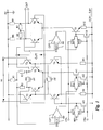
- the accurate control allows the use instead of an output bipolar transistor a resistor voltage devider to shift the output voltage level by an amount corresponding to the logical levels.
- the logical levels are chosen to be only +/-100mV, i.e., 200mV in total.
- T1 and T2 are both connected to the source of a MOS transistor M1 (metal oxide semiconductor), which drain is coupled to a negative voltage power supply, which can be operated between -2,2V and -3,6V.
- MOS transistor M1 metal oxide semiconductor
- the gate of M1 is controlled by the output of an operational amplifier OP1, which positive input is connected to the coupling point between R2, R3 and R1. Its negative input is coupled to a 200mV reference voltage that comes out of a semiconductor bandgap.
- OP1 thus controls via M1 the current that flows through the resistor voltage divider by comparing the voltage drop at resistor R2 and R3 with the reference voltage REF.
Landscapes
- Electronic Switches (AREA)
- Logic Circuits (AREA)
- Control Of Electrical Variables (AREA)
Claims (8)
- Ein Schaltkreis zum steuerbaren Schalten eines bipolaren Eingangssignals mit hoher Bitrate von einem Eingang (IN) an einen Ausgang (OUT); wobei die besagte Schaltung einen ersten (T1) und einen zweiten (T2) emittergekoppelten bipolaren Transistor umfasst, welche das Eingangssignal von dem besagten Eingang (IN) an den besagten Ausgang (OUT) übertragen, wobei der besagte erste und der besagte zweite Transistor (T1, T2) an eine konstante Stromquelle (M1) gekoppelt sind, wobei der Schaltkreis weiterhin mindestens einen Metall-Oxid-Halbleiter-Feldeffekttransistor (M2, M6, M7) zum Aktivieren oder Deaktivieren der besagten, von mindestens einem Kontrollsignal (CTRL, CTRLI) gesteuerten konstanten Stromquelle (M1) umfasst,
dadurch gekennzeichnet, dass
ein Widerstandsspannungsteller (R1, R2, R3) an die Kollektoren der besagten bipolaren Transistoren (T1, T2) gekoppelt ist, wobei die konstante Stromquelle (M1) präzise anhand einer Spannungsdifferenz zwischen einem Spannungsabfall am Widerstandsspannungsteiler und einer konstanten Referenzspannung (REF) geregelt wird, wobei der Widerstandsspannungsteiler (R1, R2, R3) die Spannung der logischen Pegel im Ausgangssignal (OUT) definiert. - Ein Schaltkreis nach Anspruch 1, wobei die konstante Stromquelle einen zweiten Metall-Oxid-Halbleiter-Feldeffekttransistor (M1) umfasst, dessen Gate von einem Operationsverstärker (OP1) gesteuert wird, dessen nicht-invertierter Eingang an den besagten Widerstandsspannungsteiler (R1, R2, R3) gekoppelt ist, und dessen invertierter Eingang an die besagte konstante Referenzspannung (REF) gekoppelt ist.
- Ein Schaltkreis nach Anspruch 1, weiterhin umfassend einen dritten (T3) und einen vierten (T4) bipolaren Transistor, welche zwischen dem besagten Eingang (IN) und der jeweiligen Basis des besagten ersten und des besagten zweiten bipolaren Transistors (T1, T2) gekoppelt sind und dadurch Emitterfolger zwischen dem besagten Eingang (IN) und dem besagten Ausgang (OUT) bilden.
- Ein Schaltkreis nach Anspruch 1, wobei der besagte erste (T1) und der besagte zweite (T2) bipolare Transistor eine erste Stufenschaltung bilden, wobei der besagte Schaltkreis weiterhin eine zweite Stufenschaltung mit einem fünften (T7) und einem sechsten (T8) emittergekoppelten bipolaren Transistor, welche einen Ausgang (OUT1) der besagten ersten Stufe mit dem besagten Ausgang (OUT) der besagten Schaltung verbinden, umfasst, wobei der besagte fünfte (T7) und der besagte sechste (T8) bipolare Transistor an eine zweite konstante Stromquelle (T9) gekoppelt ist.
- Ein Schaltkreis nach Anspruch 4, wobei die besagte zweite konstante Stromquelle einen siebten bipolaren Transistor (T9) umfasst, dessen Basis an einen zweiten Operationsverstärker (OP2) gekoppelt ist.
- Ein Schaltkreis nach Anspruch 1, weiterhin umfassend mindestens einen weiteren, an den besagten ersten und den besagten zweiten bipolaren Transistor (T1, T2) gekoppelten Feldeffekttransistor (M8, M9) zum Kurzschließen der besagten Transistoren, wenn sie abgeschaltet sind.
- Ein Schaltkreis nach Anspruch 1, wobei die besagten bipolaren Transistoren (T1-T7) aus Silizium-Germanium-Halbleiter-Verbundmaterial bestehen.
- Ein Schaltkreis nach Anspruch 2 und 5, wobei der besagte erste und der besagte zweite Operationsverstärker (OP1, OP2) mit anderen Schaltkreisen in einer Schaltmatrix geteilt werden.
Priority Applications (5)
| Application Number | Priority Date | Filing Date | Title |
|---|---|---|---|
| AT03360015T ATE454749T1 (de) | 2003-02-05 | 2003-02-05 | Ecl-schaltung mit gesteuerter stromquelle |
| DE60330836T DE60330836D1 (de) | 2003-02-05 | 2003-02-05 | ECL-Schaltung mit gesteuerter Stromquelle |
| EP03360015A EP1445863B1 (de) | 2003-02-05 | 2003-02-05 | ECL-Schaltung mit gesteuerter Stromquelle |
| US10/752,023 US7084694B2 (en) | 2003-02-05 | 2004-01-07 | Switching circuit for switching constant current source using MOS transistor |
| CNB2004100395106A CN100352162C (zh) | 2003-02-05 | 2004-02-03 | 基本交换电路 |
Applications Claiming Priority (1)
| Application Number | Priority Date | Filing Date | Title |
|---|---|---|---|
| EP03360015A EP1445863B1 (de) | 2003-02-05 | 2003-02-05 | ECL-Schaltung mit gesteuerter Stromquelle |
Publications (2)
| Publication Number | Publication Date |
|---|---|
| EP1445863A1 EP1445863A1 (de) | 2004-08-11 |
| EP1445863B1 true EP1445863B1 (de) | 2010-01-06 |
Family
ID=32605456
Family Applications (1)
| Application Number | Title | Priority Date | Filing Date |
|---|---|---|---|
| EP03360015A Expired - Lifetime EP1445863B1 (de) | 2003-02-05 | 2003-02-05 | ECL-Schaltung mit gesteuerter Stromquelle |
Country Status (5)
| Country | Link |
|---|---|
| US (1) | US7084694B2 (de) |
| EP (1) | EP1445863B1 (de) |
| CN (1) | CN100352162C (de) |
| AT (1) | ATE454749T1 (de) |
| DE (1) | DE60330836D1 (de) |
Families Citing this family (3)
| Publication number | Priority date | Publication date | Assignee | Title |
|---|---|---|---|---|
| US7821245B2 (en) * | 2007-08-06 | 2010-10-26 | Analog Devices, Inc. | Voltage transformation circuit |
| US7928765B2 (en) * | 2009-03-30 | 2011-04-19 | Lsi Corporation | Tuning high-side and low-side CMOS data-paths in CML-to-CMOS signal converter |
| CN106961271B (zh) * | 2016-01-12 | 2020-07-07 | 中芯国际集成电路制造(上海)有限公司 | 信号接收装置和信号处理设备 |
Family Cites Families (11)
| Publication number | Priority date | Publication date | Assignee | Title |
|---|---|---|---|---|
| JP2666604B2 (ja) * | 1991-05-31 | 1997-10-22 | 株式会社日立製作所 | 差動増幅器およびこれを用いたラッチ回路並びにラッチ回路を用いたメモリ装置及びその情報読み出し方法 |
| KR930008886B1 (ko) * | 1991-08-19 | 1993-09-16 | 삼성전자 주식회사 | 전기적으로 프로그램 할 수 있는 내부전원 발생회로 |
| JP2550861B2 (ja) * | 1993-05-26 | 1996-11-06 | 日本電気株式会社 | Ecl型論理回路 |
| US5614844A (en) * | 1994-01-27 | 1997-03-25 | Dyna Logic Corporation | High speed programmable logic architecture |
| JP2773692B2 (ja) * | 1995-07-28 | 1998-07-09 | 日本電気株式会社 | 入力バッファ回路 |
| JP3149759B2 (ja) * | 1995-11-17 | 2001-03-26 | 日本電気株式会社 | ラッチ回路 |
| JPH09186570A (ja) * | 1995-12-28 | 1997-07-15 | Fujitsu Ltd | 差動型電流スイッチ回路及びこれを用いたd/a変換回路並びに過渡応答低減方法 |
| JP2000306382A (ja) * | 1999-02-17 | 2000-11-02 | Hitachi Ltd | 半導体集積回路装置 |
| US6462852B1 (en) * | 1999-10-28 | 2002-10-08 | International Business Machines Corporation | Selectable low-voltage differential signal/current mode logic (LVDS/CML) receiver with the option of AC or DC coupling |
| US6342793B1 (en) * | 1999-11-03 | 2002-01-29 | International Business Machines Corporation | Method and system for sending large numbers of CMOS control signals into a separate quiet analog power domain |
| US6411159B1 (en) * | 2000-07-21 | 2002-06-25 | Stmicroelectronics, Inc. | Circuit for controlling current levels in differential logic circuitry |
-
2003
- 2003-02-05 AT AT03360015T patent/ATE454749T1/de not_active IP Right Cessation
- 2003-02-05 EP EP03360015A patent/EP1445863B1/de not_active Expired - Lifetime
- 2003-02-05 DE DE60330836T patent/DE60330836D1/de not_active Expired - Lifetime
-
2004
- 2004-01-07 US US10/752,023 patent/US7084694B2/en not_active Expired - Lifetime
- 2004-02-03 CN CNB2004100395106A patent/CN100352162C/zh not_active Expired - Fee Related
Also Published As
| Publication number | Publication date |
|---|---|
| US20040150460A1 (en) | 2004-08-05 |
| ATE454749T1 (de) | 2010-01-15 |
| US7084694B2 (en) | 2006-08-01 |
| CN100352162C (zh) | 2007-11-28 |
| CN1520034A (zh) | 2004-08-11 |
| DE60330836D1 (de) | 2010-02-25 |
| EP1445863A1 (de) | 2004-08-11 |
Similar Documents
| Publication | Publication Date | Title |
|---|---|---|
| KR900008051B1 (ko) | 논리회로 | |
| CA1135799A (en) | Switching circuit comprising a plurality of input channels and an output channel | |
| KR100242905B1 (ko) | 반도체 회로 | |
| JPH0329207B2 (de) | ||
| US4897645A (en) | Broadband signal switching equipment | |
| US5059829A (en) | Logic level shifting circuit with minimal delay | |
| US6310509B1 (en) | Differential multiplexer with high bandwidth and reduced crosstalk | |
| CA1186040A (en) | Wideband switch crosspoint and switching matrix | |
| EP1445863A1 (de) | ECL-Schaltung mit gesteuerter Stromquelle | |
| USRE35483E (en) | Switching matrix crosspoint | |
| CA1228128A (en) | Wideband switching matrix network in matrix form | |
| CA1270054A (en) | Broadband signal space switching apparatus | |
| US5349253A (en) | Logic translator interfacing between five-volt TTL/CMOS and three-volt CML | |
| US4945263A (en) | TTL to ECL/CML translator circuit with differential output | |
| JPH0310417A (ja) | Ecl/cmlエミッタホロワ電流スイッチ回路 | |
| US6504419B1 (en) | High-speed closed loop switch and method for video and communications signals | |
| US6211722B1 (en) | Low voltage high speed multiplexer and latch | |
| US5101124A (en) | ECL to TTL translator circuit with improved slew rate | |
| JPH0554757B2 (de) | ||
| WO1997027672A1 (en) | Low-power crosspoint switch | |
| US5075566A (en) | Bipolar emitter-coupled logic multiplexer | |
| DE4010283C2 (de) | ||
| US4223235A (en) | Electronic switching circuit | |
| US5132561A (en) | Switching of logic data signals | |
| JPH03277015A (ja) | Eclクランプ型カットオフドライバ回路 |
Legal Events
| Date | Code | Title | Description |
|---|---|---|---|
| PUAI | Public reference made under article 153(3) epc to a published international application that has entered the european phase |
Free format text: ORIGINAL CODE: 0009012 |
|
| 17P | Request for examination filed |
Effective date: 20030811 |
|
| AK | Designated contracting states |
Kind code of ref document: A1 Designated state(s): AT BE BG CH CY CZ DE DK EE ES FI FR GB GR HU IE IT LI LU MC NL PT SE SI SK TR |
|
| AX | Request for extension of the european patent |
Extension state: AL LT LV MK RO |
|
| AKX | Designation fees paid |
Designated state(s): AT BE BG CH CY CZ DE DK EE ES FI FR GB GR HU IE IT LI LU MC NL PT SE SI SK TR |
|
| RAP1 | Party data changed (applicant data changed or rights of an application transferred) |
Owner name: ALCATEL LUCENT |
|
| 17Q | First examination report despatched |
Effective date: 20070508 |
|
| GRAP | Despatch of communication of intention to grant a patent |
Free format text: ORIGINAL CODE: EPIDOSNIGR1 |
|
| GRAS | Grant fee paid |
Free format text: ORIGINAL CODE: EPIDOSNIGR3 |
|
| GRAA | (expected) grant |
Free format text: ORIGINAL CODE: 0009210 |
|
| AK | Designated contracting states |
Kind code of ref document: B1 Designated state(s): AT BE BG CH CY CZ DE DK EE ES FI FR GB GR HU IE IT LI LU MC NL PT SE SI SK TR |
|
| REG | Reference to a national code |
Ref country code: GB Ref legal event code: FG4D |
|
| REG | Reference to a national code |
Ref country code: CH Ref legal event code: EP |
|
| REG | Reference to a national code |
Ref country code: IE Ref legal event code: FG4D |
|
| REF | Corresponds to: |
Ref document number: 60330836 Country of ref document: DE Date of ref document: 20100225 Kind code of ref document: P |
|
| REG | Reference to a national code |
Ref country code: NL Ref legal event code: VDEP Effective date: 20100106 |
|
| PG25 | Lapsed in a contracting state [announced via postgrant information from national office to epo] |
Ref country code: SI Free format text: LAPSE BECAUSE OF FAILURE TO SUBMIT A TRANSLATION OF THE DESCRIPTION OR TO PAY THE FEE WITHIN THE PRESCRIBED TIME-LIMIT Effective date: 20100106 |
|
| PG25 | Lapsed in a contracting state [announced via postgrant information from national office to epo] |
Ref country code: AT Free format text: LAPSE BECAUSE OF FAILURE TO SUBMIT A TRANSLATION OF THE DESCRIPTION OR TO PAY THE FEE WITHIN THE PRESCRIBED TIME-LIMIT Effective date: 20100106 |
|
| PG25 | Lapsed in a contracting state [announced via postgrant information from national office to epo] |
Ref country code: PT Free format text: LAPSE BECAUSE OF FAILURE TO SUBMIT A TRANSLATION OF THE DESCRIPTION OR TO PAY THE FEE WITHIN THE PRESCRIBED TIME-LIMIT Effective date: 20100506 Ref country code: ES Free format text: LAPSE BECAUSE OF FAILURE TO SUBMIT A TRANSLATION OF THE DESCRIPTION OR TO PAY THE FEE WITHIN THE PRESCRIBED TIME-LIMIT Effective date: 20100417 Ref country code: NL Free format text: LAPSE BECAUSE OF FAILURE TO SUBMIT A TRANSLATION OF THE DESCRIPTION OR TO PAY THE FEE WITHIN THE PRESCRIBED TIME-LIMIT Effective date: 20100106 |
|
| PG25 | Lapsed in a contracting state [announced via postgrant information from national office to epo] |
Ref country code: FI Free format text: LAPSE BECAUSE OF FAILURE TO SUBMIT A TRANSLATION OF THE DESCRIPTION OR TO PAY THE FEE WITHIN THE PRESCRIBED TIME-LIMIT Effective date: 20100106 |
|
| REG | Reference to a national code |
Ref country code: CH Ref legal event code: PL |
|
| PG25 | Lapsed in a contracting state [announced via postgrant information from national office to epo] |
Ref country code: GR Free format text: LAPSE BECAUSE OF FAILURE TO SUBMIT A TRANSLATION OF THE DESCRIPTION OR TO PAY THE FEE WITHIN THE PRESCRIBED TIME-LIMIT Effective date: 20100407 Ref country code: BE Free format text: LAPSE BECAUSE OF FAILURE TO SUBMIT A TRANSLATION OF THE DESCRIPTION OR TO PAY THE FEE WITHIN THE PRESCRIBED TIME-LIMIT Effective date: 20100106 Ref country code: CH Free format text: LAPSE BECAUSE OF NON-PAYMENT OF DUE FEES Effective date: 20100228 Ref country code: CY Free format text: LAPSE BECAUSE OF FAILURE TO SUBMIT A TRANSLATION OF THE DESCRIPTION OR TO PAY THE FEE WITHIN THE PRESCRIBED TIME-LIMIT Effective date: 20100106 Ref country code: EE Free format text: LAPSE BECAUSE OF FAILURE TO SUBMIT A TRANSLATION OF THE DESCRIPTION OR TO PAY THE FEE WITHIN THE PRESCRIBED TIME-LIMIT Effective date: 20100106 Ref country code: LI Free format text: LAPSE BECAUSE OF NON-PAYMENT OF DUE FEES Effective date: 20100228 Ref country code: MC Free format text: LAPSE BECAUSE OF NON-PAYMENT OF DUE FEES Effective date: 20100301 Ref country code: SE Free format text: LAPSE BECAUSE OF FAILURE TO SUBMIT A TRANSLATION OF THE DESCRIPTION OR TO PAY THE FEE WITHIN THE PRESCRIBED TIME-LIMIT Effective date: 20100106 |
|
| PLBE | No opposition filed within time limit |
Free format text: ORIGINAL CODE: 0009261 |
|
| STAA | Information on the status of an ep patent application or granted ep patent |
Free format text: STATUS: NO OPPOSITION FILED WITHIN TIME LIMIT |
|
| PG25 | Lapsed in a contracting state [announced via postgrant information from national office to epo] |
Ref country code: CZ Free format text: LAPSE BECAUSE OF FAILURE TO SUBMIT A TRANSLATION OF THE DESCRIPTION OR TO PAY THE FEE WITHIN THE PRESCRIBED TIME-LIMIT Effective date: 20100106 Ref country code: BG Free format text: LAPSE BECAUSE OF FAILURE TO SUBMIT A TRANSLATION OF THE DESCRIPTION OR TO PAY THE FEE WITHIN THE PRESCRIBED TIME-LIMIT Effective date: 20100406 Ref country code: SK Free format text: LAPSE BECAUSE OF FAILURE TO SUBMIT A TRANSLATION OF THE DESCRIPTION OR TO PAY THE FEE WITHIN THE PRESCRIBED TIME-LIMIT Effective date: 20100106 |
|
| 26N | No opposition filed |
Effective date: 20101007 |
|
| PG25 | Lapsed in a contracting state [announced via postgrant information from national office to epo] |
Ref country code: DK Free format text: LAPSE BECAUSE OF FAILURE TO SUBMIT A TRANSLATION OF THE DESCRIPTION OR TO PAY THE FEE WITHIN THE PRESCRIBED TIME-LIMIT Effective date: 20100106 Ref country code: IE Free format text: LAPSE BECAUSE OF NON-PAYMENT OF DUE FEES Effective date: 20100205 |
|
| PG25 | Lapsed in a contracting state [announced via postgrant information from national office to epo] |
Ref country code: IT Free format text: LAPSE BECAUSE OF FAILURE TO SUBMIT A TRANSLATION OF THE DESCRIPTION OR TO PAY THE FEE WITHIN THE PRESCRIBED TIME-LIMIT Effective date: 20100106 |
|
| PG25 | Lapsed in a contracting state [announced via postgrant information from national office to epo] |
Ref country code: HU Free format text: LAPSE BECAUSE OF FAILURE TO SUBMIT A TRANSLATION OF THE DESCRIPTION OR TO PAY THE FEE WITHIN THE PRESCRIBED TIME-LIMIT Effective date: 20100707 Ref country code: LU Free format text: LAPSE BECAUSE OF NON-PAYMENT OF DUE FEES Effective date: 20100205 |
|
| PG25 | Lapsed in a contracting state [announced via postgrant information from national office to epo] |
Ref country code: TR Free format text: LAPSE BECAUSE OF FAILURE TO SUBMIT A TRANSLATION OF THE DESCRIPTION OR TO PAY THE FEE WITHIN THE PRESCRIBED TIME-LIMIT Effective date: 20100106 |
|
| REG | Reference to a national code |
Ref country code: GB Ref legal event code: 732E Free format text: REGISTERED BETWEEN 20130926 AND 20131002 |
|
| REG | Reference to a national code |
Ref country code: FR Ref legal event code: GC Effective date: 20131018 |
|
| REG | Reference to a national code |
Ref country code: FR Ref legal event code: RG Effective date: 20141016 |
|
| REG | Reference to a national code |
Ref country code: FR Ref legal event code: PLFP Year of fee payment: 13 |
|
| REG | Reference to a national code |
Ref country code: FR Ref legal event code: CA Effective date: 20150521 |
|
| REG | Reference to a national code |
Ref country code: FR Ref legal event code: CA Effective date: 20150521 |
|
| REG | Reference to a national code |
Ref country code: FR Ref legal event code: PLFP Year of fee payment: 14 |
|
| REG | Reference to a national code |
Ref country code: FR Ref legal event code: PLFP Year of fee payment: 15 |
|
| REG | Reference to a national code |
Ref country code: FR Ref legal event code: PLFP Year of fee payment: 16 |
|
| PGFP | Annual fee paid to national office [announced via postgrant information from national office to epo] |
Ref country code: GB Payment date: 20180216 Year of fee payment: 16 Ref country code: DE Payment date: 20180219 Year of fee payment: 16 |
|
| PGFP | Annual fee paid to national office [announced via postgrant information from national office to epo] |
Ref country code: FR Payment date: 20180223 Year of fee payment: 16 |
|
| REG | Reference to a national code |
Ref country code: DE Ref legal event code: R119 Ref document number: 60330836 Country of ref document: DE |
|
| GBPC | Gb: european patent ceased through non-payment of renewal fee |
Effective date: 20190205 |
|
| PG25 | Lapsed in a contracting state [announced via postgrant information from national office to epo] |
Ref country code: GB Free format text: LAPSE BECAUSE OF NON-PAYMENT OF DUE FEES Effective date: 20190205 Ref country code: DE Free format text: LAPSE BECAUSE OF NON-PAYMENT OF DUE FEES Effective date: 20190903 |
|
| PG25 | Lapsed in a contracting state [announced via postgrant information from national office to epo] |
Ref country code: FR Free format text: LAPSE BECAUSE OF NON-PAYMENT OF DUE FEES Effective date: 20190228 |