EP1445975A2 - Optischer Hochkapazitätsrouter unter Verwendung eines elektrischen Pufferspeichers - Google Patents
Optischer Hochkapazitätsrouter unter Verwendung eines elektrischen Pufferspeichers Download PDFInfo
- Publication number
- EP1445975A2 EP1445975A2 EP04001728A EP04001728A EP1445975A2 EP 1445975 A2 EP1445975 A2 EP 1445975A2 EP 04001728 A EP04001728 A EP 04001728A EP 04001728 A EP04001728 A EP 04001728A EP 1445975 A2 EP1445975 A2 EP 1445975A2
- Authority
- EP
- European Patent Office
- Prior art keywords
- optical
- header
- router
- data
- frames
- Prior art date
- Legal status (The legal status is an assumption and is not a legal conclusion. Google has not performed a legal analysis and makes no representation as to the accuracy of the status listed.)
- Granted
Links
Images




Classifications
-
- G—PHYSICS
- G02—OPTICS
- G02B—OPTICAL ELEMENTS, SYSTEMS OR APPARATUS
- G02B6/00—Light guides; Structural details of arrangements comprising light guides and other optical elements, e.g. couplings
- G02B6/24—Coupling light guides
- G02B6/26—Optical coupling means
- G02B6/28—Optical coupling means having data bus means, i.e. plural waveguides interconnected and providing an inherently bidirectional system by mixing and splitting signals
- G02B6/293—Optical coupling means having data bus means, i.e. plural waveguides interconnected and providing an inherently bidirectional system by mixing and splitting signals with wavelength selective means
-
- H—ELECTRICITY
- H04—ELECTRIC COMMUNICATION TECHNIQUE
- H04J—MULTIPLEX COMMUNICATION
- H04J14/00—Optical multiplex systems
- H04J14/02—Wavelength-division multiplex systems
- H04J14/0201—Add-and-drop multiplexing
- H04J14/0202—Arrangements therefor
- H04J14/0209—Multi-stage arrangements, e.g. by cascading multiplexers or demultiplexers
-
- H—ELECTRICITY
- H04—ELECTRIC COMMUNICATION TECHNIQUE
- H04J—MULTIPLEX COMMUNICATION
- H04J14/00—Optical multiplex systems
- H04J14/02—Wavelength-division multiplex systems
- H04J14/0227—Operation, administration, maintenance or provisioning [OAMP] of WDM networks, e.g. media access, routing or wavelength allocation
-
- H—ELECTRICITY
- H04—ELECTRIC COMMUNICATION TECHNIQUE
- H04Q—SELECTING
- H04Q11/00—Selecting arrangements for multiplex systems
- H04Q11/0001—Selecting arrangements for multiplex systems using optical switching
- H04Q11/0005—Switch and router aspects
-
- H—ELECTRICITY
- H04—ELECTRIC COMMUNICATION TECHNIQUE
- H04Q—SELECTING
- H04Q11/00—Selecting arrangements for multiplex systems
- H04Q11/0001—Selecting arrangements for multiplex systems using optical switching
- H04Q11/0062—Network aspects
- H04Q11/0066—Provisions for optical burst or packet networks
-
- H—ELECTRICITY
- H04—ELECTRIC COMMUNICATION TECHNIQUE
- H04Q—SELECTING
- H04Q11/00—Selecting arrangements for multiplex systems
- H04Q11/0001—Selecting arrangements for multiplex systems using optical switching
- H04Q11/0005—Switch and router aspects
- H04Q2011/0007—Construction
- H04Q2011/0015—Construction using splitting combining
-
- H—ELECTRICITY
- H04—ELECTRIC COMMUNICATION TECHNIQUE
- H04Q—SELECTING
- H04Q11/00—Selecting arrangements for multiplex systems
- H04Q11/0001—Selecting arrangements for multiplex systems using optical switching
- H04Q11/0005—Switch and router aspects
- H04Q2011/0007—Construction
- H04Q2011/0016—Construction using wavelength multiplexing or demultiplexing
-
- H—ELECTRICITY
- H04—ELECTRIC COMMUNICATION TECHNIQUE
- H04Q—SELECTING
- H04Q11/00—Selecting arrangements for multiplex systems
- H04Q11/0001—Selecting arrangements for multiplex systems using optical switching
- H04Q11/0005—Switch and router aspects
- H04Q2011/0007—Construction
- H04Q2011/002—Construction using optical delay lines or optical buffers or optical recirculation
-
- H—ELECTRICITY
- H04—ELECTRIC COMMUNICATION TECHNIQUE
- H04Q—SELECTING
- H04Q11/00—Selecting arrangements for multiplex systems
- H04Q11/0001—Selecting arrangements for multiplex systems using optical switching
- H04Q11/0005—Switch and router aspects
- H04Q2011/0007—Construction
- H04Q2011/0024—Construction using space switching
-
- H—ELECTRICITY
- H04—ELECTRIC COMMUNICATION TECHNIQUE
- H04Q—SELECTING
- H04Q11/00—Selecting arrangements for multiplex systems
- H04Q11/0001—Selecting arrangements for multiplex systems using optical switching
- H04Q11/0005—Switch and router aspects
- H04Q2011/0037—Operation
- H04Q2011/0039—Electrical control
Definitions
- the present invention relates to a large-capacity optical router that exchanges data traffic such as Internet protocol (IP) packets, Ethernet frames, etc., at high speed in units of optical frames, and more particularly to a large-capacity optical router using an electric buffer.
- IP Internet protocol
- the present invention further relates to an operation method.
- Gb/s gigabits/second
- Tb/s terabits/second
- a large-capacity router/switch having a capacity of several hundred Gb/s to several Tb/s is required.
- IP routers are constructed by connecting numerous small-capacity IP routers together.
- 50 ⁇ 60% of the whole capacity is used for the mutual connection of the small-capacity IP routers. This causes a waste of bandwidth and an abrupt increase of the number of IP routers according to a required capacity.
- Two conventional methods have been used to construct such large-capacity routers.
- FIG 1 is a diagram illustrating the construction of a conventional all optical router, which will be used to discuss the first method for constructing the large-capacity router.
- optical data is exchanged through a space switch 14 composed of on-off gate switches 14-3. Any collision occurring in the optical data is prevented using a variable wavelength converter and an optical-fiber delay-line buffer 16.
- the optical data is switched using a variable wavelength converter and a wavelength router such as an N ⁇ N arrayed waveguide grating (AWG). Data collision is prevented through use of an optical-fiber delay line.
- AWG N ⁇ N arrayed waveguide grating
- the second method is implemented by a large-capacity IP router adopting an interface of a speed over 10Gb/s.
- headers of input packets are recognized by packets, and the packet routing/switching is performed by driving an electric switch. Collision among the packets is prevented through an electric buffer.
- a large-capacity IP router has been developed as a kind of terabit router.
- an optical-fiber delay line is used to prevent collision among the optical data due to the absence of an optical memory.
- the length of the optical-fiber delay line may reach several tens to several hundreds of kilometers, and this causes the size of the system to be enlarged and the complexity of the system is greatly increased.
- variable wavelength converter is generally composed of a variable wavelength laser and a plurality of semiconductor optical amplifiers (SOAs). These added components cause the manufacturing cost to increase.
- the stabilization speed of the variable wavelength laser is very slow, i.e., in the range of several to several tens of milliseconds (ms), and thus it is not suitable for an optical router.
- signal performance monitoring and signal regeneration are also difficult.
- the all optical router of FIG 1 uses many optical couplers. This causes a large path loss.
- the packet forwarding is performed by recognizing the headers of the packets, there is a great difficulty in processing high-speed packets of 10Gb/s. This has limited the interface to speeds of less than 40Gb/s.
- forwarding speeds of 15 Mp/s and 60 Mp/s are required for processing 64-byte packets having speeds of 10 Gb/s and 40 Gb/s, respectively. Also, since not only add/drop packets but also path-through packets should be processed, the processing burden of the router greatly increases. This causes an inefficient use of the processing capacity.
- One embodiment of the present invention is directed to a large-capacity optical router including a plurality of input ports, a plurality of output ports, an add port for input data received from an Internet protocol (IP) router, a drop port for output data to the IP router, a wavelength division demultiplexing section for wavelength-division-demultiplexing signals input through the input ports and the add port, an input interface section for converting optical frames from the wavelength division demultiplexing section into electric signals, an optical switch for performing a high-speed switching of the optical frames output from the input interface section, an output interface section for processing the optical frames switched by and output from the optical switch, a wavelength division multiplexing section for wavelength-division-multiplexing output signals of the output interface section and transmitting the multiplexed outputs to another large-capacity optical router, a drop interface section for processing the optical frames output from the wavelength division multiplexer to the IP router, a header processing section for recognizing header information for controlling the optical router, an optical switch control section for controlling a connection state of the optical
- FIG 2 is a diagram illustrating the construction of a large-capacity optical router according to an embodiment of the present invention.
- the large-capacity optical router has N input ports INPUT 1 to INPUT N, N output ports OUTPUT 1 to OUTPUT N, an add port Add for input data received from an IP router, and a drop port Drop for output data output to the IP router.
- a wavelength division demultiplexing section 20 wavelength-division-demultiplexes wavelength signals ⁇ 1 to ⁇ N input through the input ports INPUT 1 to INPUT N and the add port Add.
- the wavelength division demultiplexing section 20 includes N+1 wavelength division demultiplexers (WDMs).
- An input interface section 30 converts optical frames input from the wavelength division demultiplexers into electric signals for processing and then converts the electric signals back to optical signals.
- N input interfaces, corresponding to the wavelength signals ⁇ 1 to ⁇ N are connected.
- An optical switch i.e., an on-off gate switch 40 performs high-speed switching of the optical frames output from the input interface section 30.
- An output interface section 50 processes the optical frames switched by and output from the optical switch 40.
- a wavelength division multiplexing section 70 wavelength-division-multiplexes the outputs of the output interface section 50 and transmits the multiplexed outputs to another large-capacity optical router.
- a drop interface section 60 processes the optical frames output from the wavelength division multiplexing section 70 to the lower IP router.
- a header processing section 75 recognizes header information for controlling the optical router.
- An optical switch control section 80 controls the connection state of the optical switch for switching the optical frames.
- a header reinserting section 90 reinserts headers into the outputs of the optical router.
- An edge traffic aggregator 100 includes an ingress part 100-1 and an egress part 100-2. The ingress part 100-1 converts IP packets input from the IP router into optical frames, and the egress part 100-2 converts the optical frames into IP packets and transmits the converted packets to the IP router.
- the ingress part 100-1 of the edge traffic aggregator 100 processes the data input from the IP router, and the egress part 100-2 of the edge traffic aggregator 100 processes the data output to the IP router.
- FIG 3 is a block diagram of the input interface section 30 of FIG 2.
- An optical receiver 120 converts an optical frame input from the wavelength division demultiplexing section into an electric signal.
- a buffer 122 stores the frame converted by the optical receiver 120 for synchronization.
- a header length detector 123 extracts a header length in order to separate a header from the converted frame.
- a switch 124 separates the header and data from the frame.
- a queue 125 stores data separated by the switch for solving the collision before the data is switched.
- An optical transmitter 126 inputs data from the queue 125, and restores the frame which has been converted into the electric signal to the optical frame in order to transmit the data to the optical switch.
- the header processing section 75 reads an address with reference to the header of the input frame. Also, the header processing section 75 decides when to output, and a new header is inserted by the header reinserting section 90.
- FIG 4 is a block diagram of the queue 125 of the input interface section 30 of FIG 3.
- the queue 125 includes a 1 ⁇ N electric switch 128, N buffers 129, and a combiner 130.
- the switch 128 switches the input data by destinations, and transmits the data to the N buffers 129.
- the number of buffers 129 should at least equal the number of destinations and receive and store the data according to destination. If the stored data are accumulated for a predetermined amount of time, the accumulated data are transmitted to the optical transmitter 126 through the combiner 125.
- the input interface section 30 is connected to the header processing section 75 for processing the separated header.
- the header processing section 75 detects the destination of the data from the header, and controls to determine an output time of the data.
- FIG 5 is a block diagram of the output interface section 50 of FIG 2.
- the output interface section 50 includes an optical receiver 140 for converting the optical data switched by the optical switch 40 into an electric signal, a buffer 141 for temporarily storing the data for a header reinsertion, a header reinserter 142 for reinserting the header, and an optical transmitter 143 for transmitting the optical data combined with the header to a next node.
- the header reinserter 142 of the output interface 50 receives the header from the header reinserting section 90 that generates the header to be reinserted.
- the header reinserting section 90 detects the destination from the header information received from the input interface section 30, and provides a new header when the data is output.
- the drop interface section 60 has the same construction as the output interface section 50 of FIG 5 except for the header reinserter 142.
- the output of the drop interface section 60 is processed again in the egress part 100-2 of the edge traffic aggregator 100, and thus the header reinserter 142 is not required.
- FIG 6 is a diagram illustrating an optical frame that is separated into a header and a data frame by the switch 124 illustrated in FIG 3.
- T HEADER denotes a header
- T DATA denotes a data frame
- T G denotes a guard time, which indicates a time when the switch 124 separates the header and the data frame from the optical frame. As illustrated in FIG 6, T G is used to prevent data loss when the switch separates the header and the data frame.
- FIG 7 is a block diagram of the ingress part 100-1 of the edge traffic aggregator 100 of FIG 2.
- the ingress part 100-1 transmits the data received from the IP router to the optical router through the add port Add.
- the ingress part 100-1 includes M optical receivers 150 for receiving packet data input from the IP router, packet processing sections 151, connected to the optical receivers 150, respectively, for performing functions such as packet forwarding and so on; an address table 152 for providing address information for the packet forwarding; an electric switch 153 for switching inputs from the packet processing sections 151 to K buffers, to be explained later, for generating the optical frame; a data frame assembler 154, provided with the K buffers, for converting the switched packets into the optical frame; a controller and scheduler 155 for determining an output order and a wavelength of the optical frame generated from the data frame assembler 154; an electric switch 156 for transmitting the optical data of which the output order and the wavelength are determined to an optical transmitting section 158, to be explained later; n header inserting sections 157 for inserting the header before an optical modulation; the optical transmitting section 158 composed of n optical transmitter
- the data frame assembler 154 divides and stores the switched packets by destinations in the n buffers. If the data is accumulated for a predetermined amount of time, it processes the data by buffers.
- the controller and scheduler 155 detects the amount of data by buffers of the data frame assembler 154, and determines the output order and the wavelength of the optical frame.
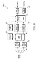
- FIG 8 is a block diagram of the egress part 100-2 of the edge traffic aggregator 100 of FIG 2.
- the egress part 100-2 receives the outputs of the drop interface section 60, and processes the data output to the lower IP router.
- the egress part 100-2 includes a wavelength division demultiplexer 160 for wavelength-division-demultiplexing the wavelength-division-multiplexed optical signal dropped by the optical router, n optical receivers 161 for converting the optical frame into an electric signal, a data frame disassembler 162 for separating the frame in units of IP packets and according to destination, a scheduler 163 for controlling an output order of the IP packets having been separated according to destination, packet processing sections 164 for processing the IP packets through a process such as forwarding and so on, an address table 165 for providing an address of the packet, an electric switch 166 for switching the processed packet to a correct destination IP router, and M optical transmitters 167 for optically modulating the switched packet.
- FIG 9 is a block diagram of another embodiment of the input interface section 30 of FIG 3. This embodiment provides additional switching efficiency for the optical router.
- a queue 185 does not provide a single output, but provides multiple (for example, K) outputs. Accordingly, the number of optical transmitters 186 at least equal the number of the outputs. In this embodiment, the data is separately transmitted according to their destinations, and thus the processing speed is improved.
- a plurality of data frames output from a plurality of buffers (not illustrated) of the queue 185 are optically modulated by the plurality of optical transmitters 186 and then input to the optical switch.
- the input interface section 30 of FIG 3 prevents a head of line (HOL) blocking problem using the multiple buffers 129 of FIG 4, but since the queue 125 provides only one output, the buffer capacity in the queue becomes large.
- HOL head of line
- multiple outputs are provided from the queue 185 with the multiple buffers as shown in FIG 9, and the buffer capacity can be reduced with a higher switching efficiency.
- the buffer capacity and the switching efficiency can be adjusted. Since the queue 185 has multiple outputs, the input interface section 30 requires a plurality of optical transmitters 186. Also, the size of the optical switch 40 should be increased by as many as K times.
- FIG 10 is a block diagram of another embodiment of the output interface section 50 of FIG 5.
- a plurality of optical receivers and buffers (for example, K optical receivers and K buffers) are provided.
- a combiner 193 is also provided.
- the data is processed according to destination, and thus the processing speed can be improved.
- IP packets transmitted from the IP router generally have wavelengths of 1.3 mm, and are converted into electric signals by the optical receiver 150 of the ingress part 100-1.
- Each converted packet is input to the packet processing section 151, which determines the destination port and the output order with reference to the address table 152.
- the data frame assembler 154 as many buffers as the number of destination addresses (for example, K) exist.
- a packet, of which the destination port and the output order have been determined by the packet processing section 151 is switched by the M ⁇ K electric switch 153 to a buffer of the data frame assembler 154 that matches the destination address.
- an output request signal is transferred to the controller and scheduler 155.
- the controller and scheduler 155 that received the output request signal confirms if an available channel exists by checking the state of the output wavelength channel. If there is no available wavelength channel, the data frame waits in the buffer until the available wavelength channel is produced. If there is an available channel, the data frame filled in the buffer is switched to the optical transmitting section 158 having the wavelength channel selected by the K ⁇ n electric switch 156. A header is then reinserted into the data frame by the header inserting section 157.
- the controller and scheduler 155 In reinserting the header, the controller and scheduler 155 generates a header signal that indicates the destination address of the data frame and so on.
- This header signal and the switched data frames are combined by the header inserting section 157, and then switched to the optical transmitter 158.
- the combined frame structure is illustrated in FIG 6.
- the header precedes the data frame by as much as the guard time.
- the header and the data frame have the fixed lengths of T H and T DF, respectively.
- the header frame of 1.25 Gb/s can be used.
- the header and the data frame have preambles, respectively.
- the optical frame is optically modulated by the optical transmitting section 158, wavelength-division-multiplexed by the wavelength division multiplexer 159, and then transmitted to the add port Add of the optical router.
- the header and the data frame are modulated with the same wavelength and then transmitted.
- the frames to be transmitted to the IP routers among the optical frames switched by the optical router are input to the egress part 100-2 of the edge traffic aggregator 100 through the drop interface section 60.
- the input optical signal is wavelength-division-demultiplexed by the wavelength division demultiplexer 160, and then converted into an electric signal by the optical receiving section 161.
- the converted data frame is separated into the original IP packet unit by the data frame disassembler 162.
- the separated IP packets are provided with output orders through the scheduler 163, processed by the packet processing section 164 with reference to the address table 165 to be transmitted to the destination IP router, and then switched by the n ⁇ M electric switch 166.
- the switched packets are transmitted to the destination IP router by the optical transmitting section 167.
- the wavelength-division-multiplexed optical frame signal output from the ingress section 100-1 of the edge traffic aggregator and the wavelength-division-multiplexed optical frames are wavelength-division-demultiplexed by the wavelength division demultiplexing section 20, and then input to the interface section 30.
- the optical frame input to the input interface section 30 is converted into an electric signal by the optical receiver 120 of FIG 3.
- the converted electric signal is input to the buffer 122 and the header length detector 123.
- the header length detector 123 recognizes the starting point and the length of the header by detecting the preamble of the header. While the header length is detected, the frame is temporarily stored in the buffer. If the detection of the starting point and the length of the header is completed, the frame stored in the buffer 122 is input to the switch 124, and separated into the header and the data frame by the switch 124 using the information on the starting point and the length of the header detected by the header length detector 123. The separated header is input to the header processing section 75, and the data frame is input to the queue 125.
- the header processing section 75 reads the information on the destination address and so on in the header separated through the forwarding process, and determines the output order of the data frame through a scheduling process.
- the data frame is stored in the queue 125 having the construction as illustrated in FIG 4 until the header processing section completes the scheduling.
- the queue 125 has n buffers 129.
- the data frame output from the queue 125 by the scheduling is optically modulated by the optical transmitter 126, and then input to the optical switch.
- the optical transmitter 126 may include inexpensive short reach type elements.
- the header processing section 75 may have a processing speed of 'data speed/n' Hz.
- the header processing section should perform a high-speed process of several tens Mp/s for processing a short-length packet of about 64 bytes.
- the header processing speed is greatly reduced in comparison to the conventional method.
- the header processing section 75 generates the control signal to the optical switch control section 80 according to the result of forwarding and scheduling, and the data frame transmitted to the optical switch 40 according to the control signal is switched at high speed to the destination. Also, the header processing section 75 transmits header change information to the header reinserting section 90 for the header reinsertion.
- the optical data frame switched by the optical switch 40 is input to the output interface section 50. This signal is then converted into an electric signal by the optical receiver 140 of FIG 5, and then stored in the buffer 141.
- the header reinserting section 90 produces a new header using the header change information transmitted from the header processing section 75, and transmits the new header signal to the header inserter 142.
- the data frame stored in the buffer 141 is output and combined with the header by the header reinserting section 90, and optically modulated by the optical transmitter 143.
- the data frame is then wavelength-division-multiplexed by the wavelength division multiplexing section 70 and is transmitted to another optical router.
- the data frame switched by the optical switch 40 is not output to another large-capacity optical router, but is output to the IP router.
- the data frame is transmitted to the egress part 100-2 of the edge traffic aggregator through the drop interface section 60 and the wavelength division multiplexing section 70. Since it is not required to insert the header to the dropped data frame, the drop interface section 60 is identical to the output interface section 50 of FIG 5 except for the header inserter 142.
- the data frames input to the egress part 100-2 of the edge traffic aggregator are processed as illustrated in FIG 5, and then transmitted to the IP router.
- the various embodiments of the present invention can solve the problems of a variable wavelength converter and an optical-fiber delay-line buffer raised in the conventional all optical router, and enable easy signal performance monitoring and easy signal reproduction.
- various embodiments of the present invention solve the limitations of forwarding and switching speeds of the conventional IP router by performing switching in units of optical frames having a predetermined length.
- the conventional IP router requires the forwarding speed of several tens of Mp/s, but the optical router according to aspects of the present invention can reduce the forwarding speed by several hundred Kp/s to several Mp/s by performing switching in units of optical frames of a predetermined length, and thus the burden of router process can be greatly lowered.
- various embodiments of the present invention reduce an upper area, construction and operation costs of a node by greatly reducing the number of elements constituting the node with a single structure having a capacity of Tb/s or more, and thus it can be expected that the present invention will be efficiently used in a large-capacity communication network.
Landscapes
- Engineering & Computer Science (AREA)
- Computer Networks & Wireless Communication (AREA)
- Signal Processing (AREA)
- Physics & Mathematics (AREA)
- General Physics & Mathematics (AREA)
- Optics & Photonics (AREA)
- Data Exchanges In Wide-Area Networks (AREA)
- Optical Communication System (AREA)
- Use Of Switch Circuits For Exchanges And Methods Of Control Of Multiplex Exchanges (AREA)
Applications Claiming Priority (2)
| Application Number | Priority Date | Filing Date | Title |
|---|---|---|---|
| KR10-2003-0006871A KR100487201B1 (ko) | 2003-02-04 | 2003-02-04 | 전기 버퍼를 이용한 대용량 광 라우터 |
| KR2003006871 | 2003-02-04 |
Publications (3)
| Publication Number | Publication Date |
|---|---|
| EP1445975A2 true EP1445975A2 (de) | 2004-08-11 |
| EP1445975A3 EP1445975A3 (de) | 2011-11-30 |
| EP1445975B1 EP1445975B1 (de) | 2013-07-10 |
Family
ID=32653329
Family Applications (1)
| Application Number | Title | Priority Date | Filing Date |
|---|---|---|---|
| EP04001728.7A Expired - Lifetime EP1445975B1 (de) | 2003-02-04 | 2004-01-27 | Optischer Hochkapazitätsrouter unter Verwendung eines elektrischen Pufferspeichers |
Country Status (5)
| Country | Link |
|---|---|
| US (1) | US7409158B2 (de) |
| EP (1) | EP1445975B1 (de) |
| JP (1) | JP3923477B2 (de) |
| KR (1) | KR100487201B1 (de) |
| CN (1) | CN100420309C (de) |
Cited By (4)
| Publication number | Priority date | Publication date | Assignee | Title |
|---|---|---|---|---|
| EP2027662A4 (de) * | 2006-04-14 | 2009-08-19 | Res & Ind Cooperation Group | Vorrichtung und verfahren zum transfer optischer daten in einem optischen vermittlungssystem |
| ITTO20090473A1 (it) * | 2009-06-22 | 2010-12-23 | St Microelectronics Srl | "trasmettitore ottico" |
| US8401388B2 (en) | 2009-06-22 | 2013-03-19 | Stmicroelectronics S.R.L. | Optical transmitter |
| CN105792032A (zh) * | 2016-04-18 | 2016-07-20 | 浙江大学 | 基于阵列波导光栅路由器的全光缓存器 |
Families Citing this family (19)
| Publication number | Priority date | Publication date | Assignee | Title |
|---|---|---|---|---|
| US6665495B1 (en) * | 2000-10-27 | 2003-12-16 | Yotta Networks, Inc. | Non-blocking, scalable optical router architecture and method for routing optical traffic |
| KR100474694B1 (ko) * | 2002-10-12 | 2005-03-10 | 삼성전자주식회사 | 버스트 데이터 통신을 위한 링형 광네트워크 |
| KR100493096B1 (ko) * | 2003-05-07 | 2005-06-02 | 삼성전자주식회사 | 고속 광 라우팅 장치 및 그 방법 |
| US7313329B2 (en) * | 2003-09-04 | 2007-12-25 | The Regents Of The University Of California | All optical variable buffer queue useful in optical packet networks |
| JP2005151259A (ja) * | 2003-11-17 | 2005-06-09 | Toshiba Corp | データ転送装置およびプログラム |
| NO327563B1 (no) * | 2004-01-20 | 2009-08-17 | Telenor Asa | En fremgangsmate og anordning for en forbedret bufferlosning i en svitsj for kommunikasjonsnettverk |
| KR100651424B1 (ko) * | 2005-07-18 | 2006-11-29 | 삼성전자주식회사 | 양방향 애드/드롭 다중화기 |
| US7602772B2 (en) * | 2005-11-30 | 2009-10-13 | Cicchetti Christopher J | High density optical network access switch |
| WO2007066757A1 (ja) | 2005-12-09 | 2007-06-14 | The Furukawa Electric Co., Ltd. | 光中継装置及び光伝送システム |
| US7801144B2 (en) * | 2006-03-31 | 2010-09-21 | Agere Systems Inc. | Switch-based network processor |
| US8175455B2 (en) | 2006-10-11 | 2012-05-08 | Nec Corporation | Optical transmission system and optical transmission control method |
| JP2010050903A (ja) * | 2008-08-25 | 2010-03-04 | Fujitsu Ltd | 伝送装置 |
| US8724988B2 (en) * | 2009-05-05 | 2014-05-13 | Telefonaktiebolaget L M Ericsson (Publ) | Synchronous packet switches |
| GB201101709D0 (en) | 2011-02-01 | 2011-03-16 | Transpacket As | A method and a node arrangement for optimizing traffic processing in integrated hybrid networks |
| KR102030573B1 (ko) * | 2014-06-03 | 2019-10-10 | 후아웨이 테크놀러지 컴퍼니 리미티드 | 광 패킷 전송 방법 및 장치, 처리 방법 및 광 스위칭 장치 |
| EP3164962B1 (de) * | 2014-07-03 | 2020-08-26 | Fiber Mountain, Inc. | Datencenterwegschalter mit verbesserter wegverbindungsarchitektur |
| EP3264644A1 (de) * | 2016-07-01 | 2018-01-03 | Nxp B.V. | Empfänger mit mehreren quellen |
| CN110460524B (zh) * | 2019-08-13 | 2022-03-25 | 上海交通大学 | 一种面向高性能计算机光电混合网络的路由策略方法 |
| CN115225585A (zh) * | 2021-04-14 | 2022-10-21 | 华为技术有限公司 | 一种dcn报文处理的方法、网络设备及系统 |
Citations (1)
| Publication number | Priority date | Publication date | Assignee | Title |
|---|---|---|---|---|
| US20020057861A1 (en) | 2000-06-08 | 2002-05-16 | An Ge | Optical IP switching router architecture |
Family Cites Families (14)
| Publication number | Priority date | Publication date | Assignee | Title |
|---|---|---|---|---|
| JP3333326B2 (ja) | 1994-08-26 | 2002-10-15 | 沖電気工業株式会社 | 光パケット交換方法および装置 |
| US6223634B1 (en) * | 1997-10-03 | 2001-05-01 | Phillips Screw Company | Recessed head fastener and driver systems |
| US6417944B1 (en) * | 1998-05-28 | 2002-07-09 | 3Com Corporation | Asynchronous transfer mode switch utilizing optical wave division multiplexing |
| JP3391291B2 (ja) * | 1999-03-30 | 2003-03-31 | 日本電気株式会社 | 光波ネットワークデータ通信方式 |
| JP3538076B2 (ja) | 1999-08-12 | 2004-06-14 | 日本電信電話株式会社 | パケット伝送装置 |
| JP3627628B2 (ja) * | 2000-06-20 | 2005-03-09 | Kddi株式会社 | 光データ伝送方法及びシステム、光送信装置及び方法並びに光交換機 |
| JP3511988B2 (ja) * | 2000-08-10 | 2004-03-29 | 日本電気株式会社 | フレーム転送装置、フレーム転送方法、フレーム転送システム |
| JP4209080B2 (ja) | 2000-11-29 | 2009-01-14 | 富士通株式会社 | 光クロスコネクト装置及び該装置を有するシステム |
| US20020118421A1 (en) | 2000-12-22 | 2002-08-29 | Yijun Xiong | Channel scheduling in optical routers |
| US6768871B2 (en) * | 2001-01-30 | 2004-07-27 | The Regents Of The University Of California | Optical layer multicasting using a multicast switch to effect survivability and security |
| US6629742B2 (en) * | 2001-02-08 | 2003-10-07 | Canon Kabushiki Kaisha | Printhead, printing apparatus using printhead, printhead cartridge, and printing element substrate |
| US6956868B2 (en) * | 2001-02-15 | 2005-10-18 | Chunming Qiao | Labeled optical burst switching for IP-over-WDM integration |
| JP2003018626A (ja) | 2001-06-29 | 2003-01-17 | Mitsubishi Electric Corp | 電気/光共用経路切替装置 |
| US7764882B2 (en) * | 2002-11-29 | 2010-07-27 | Alcatel-Lucent Usa Inc. | Optical packet tray router |
-
2003
- 2003-02-04 KR KR10-2003-0006871A patent/KR100487201B1/ko not_active Expired - Fee Related
- 2003-08-12 US US10/638,983 patent/US7409158B2/en not_active Expired - Fee Related
- 2003-09-01 CN CNB031557392A patent/CN100420309C/zh not_active Expired - Fee Related
-
2004
- 2004-01-27 EP EP04001728.7A patent/EP1445975B1/de not_active Expired - Lifetime
- 2004-02-04 JP JP2004028290A patent/JP3923477B2/ja not_active Expired - Fee Related
Patent Citations (1)
| Publication number | Priority date | Publication date | Assignee | Title |
|---|---|---|---|---|
| US20020057861A1 (en) | 2000-06-08 | 2002-05-16 | An Ge | Optical IP switching router architecture |
Cited By (5)
| Publication number | Priority date | Publication date | Assignee | Title |
|---|---|---|---|---|
| EP2027662A4 (de) * | 2006-04-14 | 2009-08-19 | Res & Ind Cooperation Group | Vorrichtung und verfahren zum transfer optischer daten in einem optischen vermittlungssystem |
| ITTO20090473A1 (it) * | 2009-06-22 | 2010-12-23 | St Microelectronics Srl | "trasmettitore ottico" |
| US8401388B2 (en) | 2009-06-22 | 2013-03-19 | Stmicroelectronics S.R.L. | Optical transmitter |
| US8401404B2 (en) | 2009-06-22 | 2013-03-19 | Stmicroelectronics S.R.L. | Optical receiver |
| CN105792032A (zh) * | 2016-04-18 | 2016-07-20 | 浙江大学 | 基于阵列波导光栅路由器的全光缓存器 |
Also Published As
| Publication number | Publication date |
|---|---|
| JP2004242320A (ja) | 2004-08-26 |
| KR20040070691A (ko) | 2004-08-11 |
| JP3923477B2 (ja) | 2007-05-30 |
| EP1445975B1 (de) | 2013-07-10 |
| US20040151171A1 (en) | 2004-08-05 |
| CN1520196A (zh) | 2004-08-11 |
| US7409158B2 (en) | 2008-08-05 |
| KR100487201B1 (ko) | 2005-05-04 |
| EP1445975A3 (de) | 2011-11-30 |
| CN100420309C (zh) | 2008-09-17 |
Similar Documents
| Publication | Publication Date | Title |
|---|---|---|
| EP1445975B1 (de) | Optischer Hochkapazitätsrouter unter Verwendung eines elektrischen Pufferspeichers | |
| KR100493096B1 (ko) | 고속 광 라우팅 장치 및 그 방법 | |
| JP3578960B2 (ja) | 超高速光パケット転送リングネットワーク、光挿入分岐型多重分離ノード装置及び光挿入分岐型多重分離ノード装置の動作方法 | |
| US7162155B2 (en) | Optical packet switching apparatus and methods | |
| CA2334549C (en) | Method and system for optical routing of variable-length packet data | |
| EP0869634A2 (de) | Wellenlängen-Multiplexing in passiven optischen Netzwerken | |
| CN100499435C (zh) | 用于突发数据通信的光多环网 | |
| US8879910B2 (en) | Optical packet switching system and optical packet transmitter device | |
| WO2013171042A1 (en) | Optical data transmission system | |
| CN107407777A (zh) | 用于光网络的系统和方法 | |
| JP2007527638A (ja) | 信号を伝送するシステムおよび方法 | |
| EP1600029A1 (de) | Architektur, verfahren und system wdm-gestützter photonischer burst-vermittelter netzwerke | |
| KR101451608B1 (ko) | 광학 패킷 스위칭 디바이스 | |
| US7272311B2 (en) | Optical ring network for burst data communication | |
| JP2002261782A (ja) | ラベルスイッチネットワークのプロテクション | |
| JP2005136951A (ja) | 光波長多重通信に用いられる光パケットルーティング装置 | |
| JP2000324162A (ja) | データ転送方法、データ転送装置及び光通信ネットワーク | |
| KR20010001698A (ko) | 부반송파 다중화 패킷 부호화를 이용한 다파장 광 패킷 교환장치 및 그 방법 | |
| Aleksić | Dynamic optical packet/burst-switched metropolitan area network | |
| JP2004266451A (ja) | 波長パス交換用トラヒックパターン変更装置および波長パス交換用トラヒックパターン変更方法 |
Legal Events
| Date | Code | Title | Description |
|---|---|---|---|
| PUAI | Public reference made under article 153(3) epc to a published international application that has entered the european phase |
Free format text: ORIGINAL CODE: 0009012 |
|
| 17P | Request for examination filed |
Effective date: 20040127 |
|
| AK | Designated contracting states |
Kind code of ref document: A2 Designated state(s): AT BE BG CH CY CZ DE DK EE ES FI FR GB GR HU IE IT LI LU MC NL PT RO SE SI SK TR |
|
| AX | Request for extension of the european patent |
Extension state: AL LT LV MK |
|
| RIN1 | Information on inventor provided before grant (corrected) |
Inventor name: OH, YUN-JE,SAMSUNG ELECTRO. CO., LTD. Inventor name: LEE, KI-CHEOL Inventor name: KIM, JONG-KWON Inventor name: DOH, SANG-HYUN |
|
| PUAL | Search report despatched |
Free format text: ORIGINAL CODE: 0009013 |
|
| AK | Designated contracting states |
Kind code of ref document: A3 Designated state(s): AT BE BG CH CY CZ DE DK EE ES FI FR GB GR HU IE IT LI LU MC NL PT RO SE SI SK TR |
|
| AX | Request for extension of the european patent |
Extension state: AL LT LV MK |
|
| RIC1 | Information provided on ipc code assigned before grant |
Ipc: H04Q 11/00 20060101AFI20111021BHEP Ipc: H04J 14/00 20060101ALI20111021BHEP |
|
| AKX | Designation fees paid |
Designated state(s): DE FR GB |
|
| 17Q | First examination report despatched |
Effective date: 20120712 |
|
| RAP1 | Party data changed (applicant data changed or rights of an application transferred) |
Owner name: SAMSUNG ELECTRONICS CO., LTD. |
|
| GRAP | Despatch of communication of intention to grant a patent |
Free format text: ORIGINAL CODE: EPIDOSNIGR1 |
|
| RIC1 | Information provided on ipc code assigned before grant |
Ipc: H04Q 11/00 20060101AFI20130117BHEP Ipc: H04J 14/02 20060101ALI20130117BHEP |
|
| RIN1 | Information on inventor provided before grant (corrected) |
Inventor name: DOH, SANG-HYUN Inventor name: KIM, JONG-KWON Inventor name: LEE, KI-CHEOL Inventor name: OH, YUN-JE |
|
| GRAS | Grant fee paid |
Free format text: ORIGINAL CODE: EPIDOSNIGR3 |
|
| GRAA | (expected) grant |
Free format text: ORIGINAL CODE: 0009210 |
|
| AK | Designated contracting states |
Kind code of ref document: B1 Designated state(s): DE FR GB |
|
| REG | Reference to a national code |
Ref country code: GB Ref legal event code: FG4D |
|
| REG | Reference to a national code |
Ref country code: DE Ref legal event code: R096 Ref document number: 602004042648 Country of ref document: DE Effective date: 20130905 |
|
| PLBE | No opposition filed within time limit |
Free format text: ORIGINAL CODE: 0009261 |
|
| STAA | Information on the status of an ep patent application or granted ep patent |
Free format text: STATUS: NO OPPOSITION FILED WITHIN TIME LIMIT |
|
| 26N | No opposition filed |
Effective date: 20140411 |
|
| REG | Reference to a national code |
Ref country code: DE Ref legal event code: R097 Ref document number: 602004042648 Country of ref document: DE Effective date: 20140411 |
|
| REG | Reference to a national code |
Ref country code: FR Ref legal event code: ST Effective date: 20140930 |
|
| PG25 | Lapsed in a contracting state [announced via postgrant information from national office to epo] |
Ref country code: FR Free format text: LAPSE BECAUSE OF NON-PAYMENT OF DUE FEES Effective date: 20140131 |
|
| PGFP | Annual fee paid to national office [announced via postgrant information from national office to epo] |
Ref country code: GB Payment date: 20161222 Year of fee payment: 14 |
|
| PGFP | Annual fee paid to national office [announced via postgrant information from national office to epo] |
Ref country code: DE Payment date: 20161220 Year of fee payment: 14 |
|
| REG | Reference to a national code |
Ref country code: DE Ref legal event code: R119 Ref document number: 602004042648 Country of ref document: DE |
|
| GBPC | Gb: european patent ceased through non-payment of renewal fee |
Effective date: 20180127 |
|
| PG25 | Lapsed in a contracting state [announced via postgrant information from national office to epo] |
Ref country code: DE Free format text: LAPSE BECAUSE OF NON-PAYMENT OF DUE FEES Effective date: 20180801 |
|
| PG25 | Lapsed in a contracting state [announced via postgrant information from national office to epo] |
Ref country code: GB Free format text: LAPSE BECAUSE OF NON-PAYMENT OF DUE FEES Effective date: 20180127 |