EP1447863A2 - Masque de gravure - Google Patents
Masque de gravure Download PDFInfo
- Publication number
- EP1447863A2 EP1447863A2 EP04003434A EP04003434A EP1447863A2 EP 1447863 A2 EP1447863 A2 EP 1447863A2 EP 04003434 A EP04003434 A EP 04003434A EP 04003434 A EP04003434 A EP 04003434A EP 1447863 A2 EP1447863 A2 EP 1447863A2
- Authority
- EP
- European Patent Office
- Prior art keywords
- pass
- aperture
- mask
- organic
- etching
- Prior art date
- Legal status (The legal status is an assumption and is not a legal conclusion. Google has not performed a legal analysis and makes no representation as to the accuracy of the status listed.)
- Withdrawn
Links
Images




Classifications
-
- H—ELECTRICITY
- H10—SEMICONDUCTOR DEVICES; ELECTRIC SOLID-STATE DEVICES NOT OTHERWISE PROVIDED FOR
- H10P—GENERIC PROCESSES OR APPARATUS FOR THE MANUFACTURE OR TREATMENT OF DEVICES COVERED BY CLASS H10
- H10P50/00—Etching of wafers, substrates or parts of devices
- H10P50/69—Etching of wafers, substrates or parts of devices using masks for semiconductor materials
- H10P50/691—Etching of wafers, substrates or parts of devices using masks for semiconductor materials for Group V materials or Group III-V materials
- H10P50/693—Etching of wafers, substrates or parts of devices using masks for semiconductor materials for Group V materials or Group III-V materials characterised by their size, orientation, disposition, behaviour or shape, in horizontal or vertical plane
- H10P50/695—Etching of wafers, substrates or parts of devices using masks for semiconductor materials for Group V materials or Group III-V materials characterised by their size, orientation, disposition, behaviour or shape, in horizontal or vertical plane characterised by the process involved to create the mask, e.g. lift-off masks or sidewalls or to modify the mask
-
- H—ELECTRICITY
- H10—SEMICONDUCTOR DEVICES; ELECTRIC SOLID-STATE DEVICES NOT OTHERWISE PROVIDED FOR
- H10K—ORGANIC ELECTRIC SOLID-STATE DEVICES
- H10K71/00—Manufacture or treatment specially adapted for the organic devices covered by this subclass
- H10K71/20—Changing the shape of the active layer in the devices, e.g. patterning
- H10K71/231—Changing the shape of the active layer in the devices, e.g. patterning by etching of existing layers
- H10K71/233—Changing the shape of the active layer in the devices, e.g. patterning by etching of existing layers by photolithographic etching
-
- H—ELECTRICITY
- H10—SEMICONDUCTOR DEVICES; ELECTRIC SOLID-STATE DEVICES NOT OTHERWISE PROVIDED FOR
- H10P—GENERIC PROCESSES OR APPARATUS FOR THE MANUFACTURE OR TREATMENT OF DEVICES COVERED BY CLASS H10
- H10P50/00—Etching of wafers, substrates or parts of devices
- H10P50/20—Dry etching; Plasma etching; Reactive-ion etching
- H10P50/24—Dry etching; Plasma etching; Reactive-ion etching of semiconductor materials
- H10P50/242—Dry etching; Plasma etching; Reactive-ion etching of semiconductor materials of Group IV materials
-
- H—ELECTRICITY
- H10—SEMICONDUCTOR DEVICES; ELECTRIC SOLID-STATE DEVICES NOT OTHERWISE PROVIDED FOR
- H10P—GENERIC PROCESSES OR APPARATUS FOR THE MANUFACTURE OR TREATMENT OF DEVICES COVERED BY CLASS H10
- H10P50/00—Etching of wafers, substrates or parts of devices
- H10P50/69—Etching of wafers, substrates or parts of devices using masks for semiconductor materials
- H10P50/691—Etching of wafers, substrates or parts of devices using masks for semiconductor materials for Group V materials or Group III-V materials
- H10P50/692—Etching of wafers, substrates or parts of devices using masks for semiconductor materials for Group V materials or Group III-V materials characterised by their composition, e.g. multilayer masks or materials
-
- H—ELECTRICITY
- H10—SEMICONDUCTOR DEVICES; ELECTRIC SOLID-STATE DEVICES NOT OTHERWISE PROVIDED FOR
- H10P—GENERIC PROCESSES OR APPARATUS FOR THE MANUFACTURE OR TREATMENT OF DEVICES COVERED BY CLASS H10
- H10P76/00—Manufacture or treatment of masks on semiconductor bodies, e.g. by lithography or photolithography
- H10P76/40—Manufacture or treatment of masks on semiconductor bodies, e.g. by lithography or photolithography of masks comprising inorganic materials
- H10P76/405—Manufacture or treatment of masks on semiconductor bodies, e.g. by lithography or photolithography of masks comprising inorganic materials characterised by their composition, e.g. multilayer masks
-
- H—ELECTRICITY
- H10—SEMICONDUCTOR DEVICES; ELECTRIC SOLID-STATE DEVICES NOT OTHERWISE PROVIDED FOR
- H10P—GENERIC PROCESSES OR APPARATUS FOR THE MANUFACTURE OR TREATMENT OF DEVICES COVERED BY CLASS H10
- H10P76/00—Manufacture or treatment of masks on semiconductor bodies, e.g. by lithography or photolithography
- H10P76/40—Manufacture or treatment of masks on semiconductor bodies, e.g. by lithography or photolithography of masks comprising inorganic materials
- H10P76/408—Manufacture or treatment of masks on semiconductor bodies, e.g. by lithography or photolithography of masks comprising inorganic materials characterised by their sizes, orientations, dispositions, behaviours or shapes
- H10P76/4085—Manufacture or treatment of masks on semiconductor bodies, e.g. by lithography or photolithography of masks comprising inorganic materials characterised by their sizes, orientations, dispositions, behaviours or shapes characterised by the processes involved to create the masks
Definitions
- the present invention relates to patterning methods used in the manufacture of organic electroluminescence elements and the like, and particularly relates to etching masks.
- Organic electroluminescence elements are known as elements that make use of organic compound material thin-films (hereafter, referred to as “organic films”) that provide electroluminescence. (hereafter, referred to as "EL”) by the injection of an electric current.
- Organic EL elements are made up of, for example, a transparent electrode, one or more organic films, and a metal electrode layered in order on a transparent substrate.
- An organic EL display panel that has a plurality of organic EL elements as light emitting portions, a matrix-type display panel for example, is made up of horizontal line electrodes including a transparent electrode layer, one or more organic films, and vertical column electrodes that intersect with the line electrodes and include a metal electrode layer, layered in order.
- Each of the line electrodes is formed in a band shape, and the line electrodes are arranged parallel to each other with predetermined spacings.
- the column electrodes are likewise arranged.
- a matrix-type display panel is provided with a picture display arrangement made up of light emitting pixels of a plurality of organic EL elements formed at the intersecting portions of the plurality of line and column electrodes.
- an organic film is formed after a transparent electrode layer is formed on a transparent substrate.
- the organic film is formed by vapor deposition or the like with one or more layers of thin film corresponding to light emitting pixels.
- a resist is applied to a thin film formed on a substrate, and then the resist is exposed. After that, a resist mask is formed by dissolving the resist exposure portions of a predetermined pattern in a developer solution (positive type), or by the resist portions becoming difficult to dissolve (negative type), and by etching the thin film, patterns are formed with portions that are etched and portions that are not etched.
- thin film is vaporized and stripped by irradiating focused laser light onto the thinfilm,and byselectively repeating this procedure, patterns are formed with portions that are stripped and portions that are not stripped.
- an organic film on electrode lead portions must be removed in order to achieve contact with the first display electrodes. For this reason, patterning is performed with a stripping process such as that described above.
- Photolithography cannot be used with organic films that are susceptible to solvents such as developer solutions. Furthermore, with laser ablation methods, the focus range of the laser is from several tens to several hundreds of microns ( ⁇ m) at best, and has the drawback of requiring considerable time when performing patterning process on large areas.
- the present invention provides a dry etching mask that enables accurate pattern formation of organic films and the like used in organic EL elements and the like, a patterning method using the same, an organic EL element with which manufacturing efficiency can be improved, and a manufacturing method for such display panels.
- an etching mask having a pass-through aperture for exposing only a surface to be etched, which comprises a protruding periphery portion that protrudes at the periphery of the pass-through aperture, and a recessed portion enclosed by the protruding periphery portion.
- a thin film pattern forming method for forming a predetermined pattern on a thin film which comprises forming at least one thin film on a substrate; and performing a dry etching process for placing a dry etching mask on the at least one thin film that has been formed and for applying an etching gas thereto; wherein the dry etching mask is provided with a pass-through aperture for exposing only a surface to be etched, and is provided with a protruding periphery portion that protrudes at the periphery of the pass-through aperture, and a recessed portion enclosed by the protruding periphery portion.
- an organic electroluminescence element comprising at least one organic film that is placed between electrode layers and provides electroluminescence, which comprises forming at least one organic film on a substrate; and performing a dry etching process for placing a dry etching mask on the at least one organic film that has been formed and for applying an etching gas to at least one of the at least one organic film; wherein the dry etching mask is provided with a pass-through aperture for exposing only a surface to be etched, and is provided with a protruding periphery portion that protrudes at the periphery of the pass-through aperture, and a recessed portion enclosed by the protruding periphery portion.
- an organic electroluminescence element that is manufactured through an organic electroluminescence element manufacturing method having steps of forming at least one organic film on a substrate on which an electrode layer has been pre-laid; and performing a dry etching process for placing a dry etching mask on the at least one organic film that has been formed and for applying an etching gas thereto, which comprises at least one electroluminescence film provided the electrode layer and any other subsequently formed electrode layer; wherein the dry etching mask is provided with a pass-through aperture for exposing only a surface to be etched, and is provided with a protruding periphery portion that protrudes at the periphery of the pass-through aperture, and a recessed portion enclosed by the protruding periphery portion.
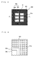
- FIG. 1 shows a dry etching mask (hereinafter, also simply referred to as "mask”) 30 of a first embodiment of the present invention.
- FIG. 1 shows a schematic plan view of a mask seen from the side of the object to be etched.
- the mask 30 is made up of a blocking portion 30a that covers surfaces other than those that are to be etched, and pass-through apertures 31 that enable the exposure of surfaces that are to be etched.
- the blocking portion 30a is provided with periphery portions 30b that protrude at the peripheries of the pass-through apertures 31, and contact and enclose areas other than those that are to be etched, and a recessed portion 30c enclosed by the periphery portions 30b.
- the periphery portions 30b have a thickness L that is greater than the thickness B of the recessed portion 30c of the blocking portion 30a.
- the mask 30 is provided with a plurality of pass-through apertures 31 so that etching gas can pass through.
- the mask 30 is made of a metal such as nickel or stainless steel (SUS) for example.
- the areas under the pass-through apertures 31 are etched when dry etching is performed while the mask 30 makes contact on a thin film 2 formed on a substrate, but the areas under the blocking portion 30a, including the receded (depression) portions 30c, are not etched and remain.
- the contact regions with the thin film 2 formed on the substrate are only where the protruding portions (i.e., periphery portions 30b) of the blocking portion 30a make contact with a portion of the thin film 2 as shown in FIG. 2. Therefore, due to the recessed portions 30c, the blocking portion 30a does not contact the film, and there causes no damage on the thin film 2. This is effective in such cases as when the thin film to be etched is easily damaged, or when forming further layer (s) of thin film on residual areas after etching.
- FIG. 3 shows a dry etching mask 300 according to a second embodiment (hereinafter, referred to as "second mask 300").
- Fig. 3 shows a schematic plan view of a mask seen from side the of the object to be etched.
- the second mask 300 is a reversed mask of the mask 30 of the first embodiment described above.
- the second mask 300 is providedwith ablockingportion 30a including protruding periphery portions 30b and recessed portions 30c, as well as pass-through apertures 31 that are similar to those in the first embodiment.
- the pass-through apertures 31 are covered by a so-called mesh mask, which is a mesh structure 301.
- the mesh structure 301 has a plurality of pass-through holes 31a (or, net holes). Each of the plurality of pass-through holes 31a has a surface area smaller than the surface area of the pass-through apertures 31.
- the protruding portions (i.e., periphery portions 30b) of the blocking portion 30a that is integrated with the mesh structure 301 contacts only a portion of the thin film 2 formed on the substrate, and the recessed portions 30c of the blocking portion 30a do not contact the thin film formed on the substrate.
- freely shaped patterning can be realized with the mesh mask 301 which has pass-through apertures 31 formed as a net or mesh. If the distance between the net and the surface to be etched is small, that is, if the thickness L of the periphery portion 30b is insufficient, the plasma gas or other such etching gas does not circulate well behind the net of the aperture portions (on the thin film side), and there may be a residual, net-shaped thin film 2.
- the thickness L of the periphery portion 30b must be equal to or greater than the line width of the mesh mask.
- the mesh density of the mask is preferably 10-mesh to 1, 000-mesh, or more preferably, 100-mesh to 1,000-mesh.
- Material that has resistance to etching gases is used for the material of the mesh structure 301 and the blocking portions 30a.
- metals such as austenitic stainless steel (SUS) are used in plasma ashing equipment.
- a patterning method using dry etching with a conventional etching mask has a problem of the etching mask bending because of insufficient mask strength, for example, when the mask pattern is such that aperture portions are large with a fine island-shape pattern of multiple light emitting portions, or with a striped pattern, but the blocking portion is of a fine pattern. Thus, fine patterns cannot be formed.
- the stiffness of the etching mask can be improved, and fine island-shape patterns and line-and-space patterns can be formed.
- a thin film 2 is formed on a substrate 1 such as a glass resistant to etching gases.
- the deposited thin film 2 may be organic or inorganic.
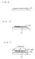
- the mask 30 of the first embodiment is brought into contact with the thin film 2 on the substrate 1 as shown in FIG. 7, and the areas below the pass-through apertures 31 are etched by being exposed to an etching gas atmosphere.
- the substrate 1 under the pass-through apertures 31 is exposed as shown in FIG. 8.
- the surface of the thin film 2 remaining under the blocking portions 30a is not damaged, since the mask 30 is depressed or concave-shaped.
- Organic EL element manufacturing method including dry etching process
- a first display electrode E1 which is resistant to dry etching is formed on a glass substrate.
- the film forming method at this stage may be a wet process such as a spin coating method, or a screen printing method or the like, or a dry process such as vacuum vapor deposition. Furthermore, it may be a polymeric material layer and/or a non-polymeric material layer. It is also possible to form all layers up to the organic light emitting layer at this stage.
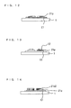
- a second mask 300 is placed on the organic film 21 as shown in FIG. 11, and dry etching is performed using the mask. After dry etching has been performed for all organic films, patterning is performed to form organic film pattern 21p as shown in FIG. 12.
- a second display electrode E2 is formed on the organic film pattern 21p as shown in FIG. 13.
- a second organic film 21p2 (which may include a plurality of layers) is formed on the first organic film as a pattern using a vacuum vapor deposition device or the like, and using a mask or the like.
- the second display electrode E2 is formed on the second organic film 21p2 as shown in FIG. 15.
- a passive matrix organic EL display panel has been manufactured with an organic EL element manufacturing method that uses a mask according to the second embodiment.
- first and second display electrodes since light emitting portions are defined at the intersecting portions of the line electrodes and column electrodes, that is, the first and second display electrodes, a plurality of first display electrodes (anodes) that extend parallel to each other are formed on a transparent substrate as follows.
- a transparent glass substrate was prepared, and indium tin oxide (hereinafter, referred to as "ITO") was formed on the main surface thereof by sputtering to a film thickness of 1, 500 angstroms (A). Then, a stripe-shaped pattern was formed on the ITO film using a photoresist AZ6112 made by Tokyo Ohka Kogyo Co. , Ltd. The substrate was immersed in a mixture of an aqueous solution of ferric chloride and hydrochloric acid, and portions of the ITO film not covered by the resist were etched. Finally, the substrate was immersed in acetone and the resist was removed, thus obtaining a pattern of a plurality of parallel first display electrodes.
- ITO indium tin oxide
- a coating solution obtained by dissolving an acid-doped polyaniline derivative in an organic solvent was spin-coated on the entire surface of the first display electrodes of the substrate obtained in the step of forming the first display electrodes to form a film.
- the substrate was heated on a hot plate to vaporize the solvent, thus obtaining a polyaniline film with a film thickness of 450 angstroms (A) on the first display electrodes.
- a mesh mask of the second embodiment was placed at a predetermined position on the polyaniline film on the substrate obtained in the step of forming a conductive, polymeric film.
- the substrate to which the mesh mask is attached was put into a plasma ashing equipment, and etching was performed for 4 minutes under conditions of plane-parallel anode coupling, RF 1,000 W, O 2 : 225 sccm, Ar: 75 sccm, pressure: 62 Pa, 80oC, then the mesh mask was removed.
- the polyaniline film portions under the aperture portions of the mesh mask were completely removed, and the patterns of a portion of the first display electrodes were exposed, while the portions of polyaniline film that were to become the display portions of the organic EL element remained undamaged under the blocking portions. It should be noted that the protruding portion of the mesh mask was formed so that light emitting portions were avoided.
- the plasma ashing equipment was a resist stripping equipment, in which a reaction was caused between a plasma gas and the resist, and the resist was vaporized and removed.
- an organic material such as a resist material becomes CO 2 , H 2 O, O 2 or the like that chemically reacts with oxygen plasma to be gaseous and removed from the substrate.
- NPABP 4,4'-bis [N-(1-naphthyl)-N- phenylamino]) biphenyl
- Alq3 tris (8-hydroxyquinoline) aluminum
- a plurality of second display electrodes (cathodes) extending parallel to each other and perpendicular to the first display electrodes were formed on the organic films on the substrate obtained in the step of organic film formation.
- stripes of an Al-Li alloy with a film thickness of 1,000 angstroms were formed by a deposition method at predetermined positions on the Alq3 film, thus a plurality of organic EL elements arranged in a matrix were completed on the substrate.
- the light emitting performance of the sealed organic EL display panel was excellent, and defects such as dark spots, particle adherence, and damage to the organic film were not observed, since the mask was not brought into contact with the organic film.
- the present invention can be applied to an active matrix organic EL display panel.
- the embodiment was described in terms of the simplest structure of an organic EL element made up of the first display electrodes, the organic film, and the second display electrodes, but it is also possible to provide other components on the substrate, for example, the barrier walls disclosed in Japanese Patent Applications Nos. H08-315981 and H08-227276. In this case, these components are not easily damaged, and the present invention is even further effective.
- an auxiliary protruding portion 30D is provided at a non-light emitting portion at the recessed portion enclosed by the periphery portion.
- the auxiliary protruding portion 30D may also be applied when there is no mesh structure 301, as well as a case in which the mesh structure 301 is provided.
- a grounding portion 310 may be provided that is connected to a portion of the mask, for example, the blocking portion 30a as shown in FIG. 17, grounding the mask to the electrodes of the plasma ashing equipment.
- the recessed portions of the mask do not come in contact with the substrate, and consequently there is no particle adherence to the organic film, and no damage to the organic film, and therefore it is possible to provide an organic EL display panel having organic EL elements that can provide excellent display without defects.
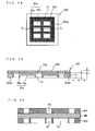
- Fig. 18 shows a mask 330 for dry etching (hereinafter, referred to as the third mask 330) according to the third embodiment of the present invention.
- Fig. 18 shows a schematic plan view of a mask seen from side of the object to be etched.
- Six blocking portions 30a in a central area correspond to the portions where the thin film should be remained after etching.
- a blocking portion 30ap on a peripheral portion serves as a frame body which contacts with the substrate (or with the film which formed on the substrate and to be processed) so as to increase the contact area of the substrate and the third mask 330 to obtain stable contact therebetween.
- Fig. 19 shows a cross sectional view along the line AA of the third mask 330 shown in Fig. 18.
- the third mask 330 has a structure in which the discrete members, that is, the mesh structure 301 and the blocking portion 30a are integrally coupled.
- the blocking portion and the mesh structure 301 of the third mask 330 are attached together in which the blocking portion has a thickness t2 and the mesh structure 301 has a thickness t1, the mesh structure 301 including a recessed portion having a depth "d".
- the blocking portion 30ap in a peripheral portion is formed so as not have a recessed portion on the side at which the mask 330 contacts with the substrate, for the purpose of increasing the strength of the third mask 330.
- the third mask 330 can be manufactured, for example, in the following manufacturing process.
- resist patterns RP1, RP2 are respectively formed on the sides of a mask mother matrix MM of a plane plate made up of stainless steel, for example.
- a resist pattern RP1 there is provided in a resist pattern RP1 an aperture P1 for exposing only the surface which should be etched (which corresponds to the pass-through aperture 31 in Fig. 19).
- apertures P2and P3 for exposing only the surface which should be etched (which correspond to the pass-through aperture 31 and the recessed portion 30c of Fig. 19).
- a wet etching processing is performed on both sides of the mask mother matrix MM.
- the maskmother matrixMM is etched on both sides thereof using a solution including a material, for example, an acid to dissolve the mask mother matrix MM.
- the pass-through apertures 31 and the recessed portions 30c are formed by etching.
- the etching is finished when the depth of the recessed portion 30c is reached a desired depth and the portion of the aperture 31 is penetrated through.
- the patterned resist on both sides of the mask mother matrix MM is stripped off.
- the patterned resist can be stripped off by using, for example, an alkali solution, an organic solvent or an oxygen plasma processing. Accordingly, there is provided the mask mother matrix MM which has a blocking portion 30ap on the periphery, a pass-through aperture 31 and a recessed portion 30c.
- a mesh structure 301 is attached to the obtained mask mother matrix MM. Then, a mesh structure 301 which is manufactured in another manufacturing process is attached by an adhesive or by means of a plating processing on the opposite side of the blocking portion 30ap in a peripheral portion and the recessed portion 30c of the blocking portion 30a.
- the third mask 330 is provided as shown in Fig. 19.
- the mesh structure 301 can be manufactured with the similar etching process. Alternatively, the mesh structure 301 can be manufactured by means of electroforming (plating) technology. Furthermore, the mesh structure 301 can be manufactured by combining wires consisting of, for example, metal or fiber.
- the blocking portion 30a can be formed by using an electroforming technique.
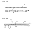
- Fig. 25 shows a cross sectional view of a fourth mask 340.
- the fourth mask 340 has a structure in which the mesh structure 301 and the blocking portion 30a are formed by etching in one piece, but not formed as an integral of the discrete members.
- the mesh structure 301 is formed in only the pass-through aperture 31 between the blocking portion 30ap of a peripheral portion and the blocking portion 30a.
- Total thickness of the fourth mask 340 is t1, and a recessed portion of depth "d" is provided in the blocking portion 30a. It is preferable that the blocking portion 30ap in a peripheral portion is formed so as not have a recessed portion on the side at which the fourth mask 340 contacts with the substrate, for the purpose of increasing the strength of the fourth mask 340.
- the fourth mask 340 can be manufactured, for example, in the following manufacturing process.
- resist patterns RP1, RP2 are respectively formed on the sides of a mask mother matrix MM of a plane plate made up of, for example, stainless steel.
- a resist pattern RP1 an aperture P4 for exposing only the surface which should be etched (which corresponds to the pass-through hole 31a in Fig. 25).
- apertures P2and P3 for exposing only the surface which should be etched (which correspond to the pass-through aperture 31 and the recessed portion 30c in Fig. 25).
- a wet etching processing is performed on both sides of the mask mother matrix MM.
- the mask mother matrix MM is etched on both sides thereof using a solution including a material, for example, an acid to dissolve the mask mother matrix MM.
- the pass-through hole 31a, the pass-through aperture 31 and the recessed portion 30c are formed by etching.
- the etching is finished when the depth of the recessed portion 30c is reached a desired depth and the portions of the pass-through hole 31a and the aperture 31 are penetrated through.
- the patterned resist on both sides of the mask mother matrix MM is stripped off.
- the patterned resist can be stripped off by using, for example, an alkali solution, an organic solvent or an oxygen plasma processing. Accordingly, there is provided the mask mother matrixMM, as shown in Fig. 25, which has the blocking portion 30ap on the periphery, the mesh structure 301, the pass-through aperture 31 and the recessed portion 30c.
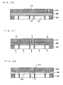
- a first photo resist pattern PP1 is formed on the principal surface of a mask mother die MD of a plane plate made up of, for example, stainless steel.
- a first photo resist pattern PP1 apertures OP, OP0, OP1 for exposing only the surfaces (which correspond to the mesh structure 301, the blocking portion 30ap on the periphery and the blocking portion 30a in Fig. 25) on which metal should be precipitated or deposited, while the other area is covered.
- an electroforming tank (not shown) provided with an anode therein filled with a solution including nickel ions.
- the mother die MD is dipped in the electroforming tank.
- the mother die MD is used as a cathode, and a direct current is passed through between the cathode and the anode for a predetermined time period.
- Electrodeposition of nickel (Ni) is performed in an exposed surface of the mother die MD to form a metal layer ML of nickel having a thick wall thickness.
- the mother die MD is taken out from the electroforming tank to be washed when the thickness of the metal layer ML for the recessed portion of the blocking portion and the mesh structure became a predetermined film thickness (t1-d).
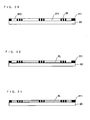
- a second photo resist pattern PP2 is formed on the first photo resist pattern PP1 and the metal layer ML formed on the mother die MD.
- apertures OP2 and OP3 are provided, in the second photo resist pattern PP2, apertures OP2 and OP3 for exposing only the surfaces (which correspond to the blocking portion 30ap on the periphery and the periphery portion 30b of the blocking portion in Fig. 25) on which metal should be deposited, while the other area is covered.
- the mother die MD having the second photo resist pattern PP2 thereon is dipped in the electroforming tank which provided with an anode therein filled with a solution including nickel ions in a similar manner as described above.
- the mother die MD is used as a cathode, and a direct current is passed through between the cathode and the anode for a predetermined time period.
- Electrodeposition of nickel (Ni) is performed on the exposed surface of the mother die MD to form a metal layer ML2 of nickel having a thick wall thickness.
- the mother die MD is taken out from the electroforming tank to be washed when the total thickness of the metal layer ML1 and the metal layer ML2 for the blocking portion on the periphery and the periphery portion became a predetermined total film thickness.
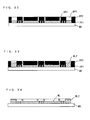
- the first and second photo resist patterns are stripped off by using, for example, an alkali solution, an organic solvent or an oxygen plasma processing.
- the fourth mask with electroforming (precipitation method) in the present embodiment When producing the fourth mask with electroforming (precipitation method) in the present embodiment, a high processing accuracy of a range of ⁇ 1 micrometer ( ⁇ m) is possible, thereby thickness precision can be improved.
- Step 1 Manufacturing of the mesh structure 301
- Electroforming of Ni in a mesh shape was performed on a mother die made of stainless steel. Only the mother die was removed to fabricate a mesh structure (which corresponds to top half in Fig. 19).
- the fabricated mesh structure had a thickness (corresponds to "t1" in Fig. 19) of 0.2mm, a dimension of 50mm ⁇ 50mm, and an L/S of 0.025mm/0.038mm (equivalent to 400-mesh).
- Step 2 Manufacturing of the blocking portion
- Step 1 electroforming of Ni was performed on a mother die twice of stainless steel to form a blocking portion pattern (equivalent to bottom half in Fig. 19) having a recessed portion such that the recessed portion was facing to the mother die.
- the fabricated blocking portion had a thickness (corresponds to "t2" in Fig. 19) of 0.2mm, a dimension of 12mm ⁇ 9mm.
- the depth of the recessed portion (corresponds to "d” in Fig. 19) was 0.1mm and the dimension was 11.6mm ⁇ 8.6mm. In other words, the width of the periphery portion that contacted with the substrate was 0.1mm.
- Electroforming of Ni was performed on the mesh structure and the blocking portion which were manufactured in Step 1 and Step 2, while the mesh structure and the blocking portion were attached together and fixed to be integrally formed. Then, the mother die of the blocking portion was taken away. The line width of the mesh structure was broadened and an L/S was 0.029mm/0.034mm.
- a reinforcement frame made up of stainless steel having a thickness of 2mm, a dimension of 50mm ⁇ 50mm and a frame width of 3mm is fixed to a periphery of the mask (on the mesh structure of the blocking portion of the peripheral portion) which was manufactured in Step 3 with an adhesive to increase strength of the mask, thus the etching mask of the embodiment was completed.
- Step 1 Formation of polyaniline thin film
- a glass substrate was washed well and a spin coating of a polyaniline solution which is doped with acid was performed on the glass substrate. After the spin coating, the glass substrate was dried with heating to form a polyaniline film of about 25 nm.
- Step 2 Dry etching
- the mask manufactured in the Embodiment-1 was fixed on the glass substrate formed in Step 1 with screws while the mask was brought into intimate contact with the glass substrate. Then, dry etching processing under various kinds of conditions was performed on the polyaniline film using a plasma equipment (a dry etching equipment) V -1000 made by Mori engineering Co., Ltd.
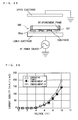
- etching processing was summarized in the following Table 1 and the schematic drawing for illustrating the etching processing is shown in Fig. 35.
- the substrate was arranged on a lower electrode as shown in Fig. 35.
- each of the lower electrode and the upper electrode had the size of 280mm ⁇ 280mm, and the distance between the lower and upper electrodes was 40mm.
- the frequency of the high-frequency (RF) power supply used was 13.6MHz.
- the etching processing was performed in two modes in the present embodiment, that is, in a mode in which the RF power supply was connected to the lower electrode as shown in Fig. 35 (hereinafter, referred to as RIE mode), and in a mode in which the RF power supply was connected to the upper electrode (hereinafter, referred to as DP mode).
- RIE mode a mode in which the RF power supply was connected to the lower electrode as shown in Fig. 35
- DP mode a mode in which the RF power supply was connected to the upper electrode
- the substrate temperature is easily increased so that caution must be taken. For example, there will be a case in which the substrate must be cooled when using a substrate or a film of low heat resistance.
- the DP mode plasma occurs on the upper electrode side, i.e., at a distance away from the substrate. Therefore, a rise of the substrate temperature can be suppressed, although the etching rate is low.
- the result can be analyzed as follows.
- etching with a mixed gas of an inert gas such as Ar and a gas which is reactive with the organic layer in order to perform uniform etching and to achieve a high etching rate. Uniformity of etching can be achieved by coming around of the etching gas at the backside of the net.
- ITO On a grass substrate having the size of 30mm x 30mm, ITO was formed in a stripe pattern of 2mm width.
- Step 2 Formation of Polyaniline film as a hole injection layer
- the glass substrate of Step 1 was washed well and a spin coating of a polyaniline solution which is doped with acid as hole injection layer was performed on the glass substrate. After the spin coating, the glass substrate was dried with heating to form a polyaniline film of about 25 nm.
- Etching of polyaniline film was performed in a similar manner to that of the Embodiment-2.
- the etching condition used was a condition D of Table 1.
- Step 4 Manufacturing of the other layers in the organic EL device
- NPABP of 45 nm, Alq3 of 60 nm and Li 2 O of 1 nm were formed by vacuum deposition with the use of a mask. Further, as the cathode, Al stripes each having 2mm width were formed by vacuum deposition along the orthogonal direction to the ITO.
- An organic EL device of the embodiment was fabricated in much the same way as in Embodiment-3 except that the etching condition of the polyaniline was performed with condition H of Table 1 at Step 3 in Embodiment-3.
- An organic EL device of the embodiment was fabricated in much the same way as in 3) of Embodiment-3 except that the patterning of the polyaniline was performed by wiping with a wiper.
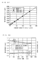
- Figs. 36 and 37 The measurement result on the initial characteristics of the organic EL devices fabricated as described above are shown in Figs. 36 and 37.
- brightness degradation characteristics is shown in Fig. 38 when the devices were driven with a DC current of 210mA/cm2.
- the devices of Embodiment-3 and Embodiment -4 showed the approximately the same characteristic as that of the comparative example 1. Therefore, it is found that the etching method in the embodiments did not exert an adverse influence on the organic layers which composed the organic EL devices. The reason is considered that the blocking portions of the mask prevented the incidence of high energy particles, for example, secondary electrons or ions of O 2 and Ar into the polyaniline layers.
- a blocking portion of a mask it is necessary for a blocking portion of a mask to use the materials which can prevent these high energy particles which are generated in the etching processing. It is preferable to use an electrically conductive material such as metal since the material captures charged particles or ions.
Landscapes
- Engineering & Computer Science (AREA)
- Manufacturing & Machinery (AREA)
- Electroluminescent Light Sources (AREA)
- Particle Formation And Scattering Control In Inkjet Printers (AREA)
Applications Claiming Priority (4)
| Application Number | Priority Date | Filing Date | Title |
|---|---|---|---|
| JP2003037932 | 2003-02-17 | ||
| JP2003037932 | 2003-02-17 | ||
| JP2004026888A JP2004273438A (ja) | 2003-02-17 | 2004-02-03 | エッチング用マスク |
| JP2004026888 | 2004-02-03 |
Publications (2)
| Publication Number | Publication Date |
|---|---|
| EP1447863A2 true EP1447863A2 (fr) | 2004-08-18 |
| EP1447863A3 EP1447863A3 (fr) | 2009-07-22 |
Family
ID=32684295
Family Applications (1)
| Application Number | Title | Priority Date | Filing Date |
|---|---|---|---|
| EP04003434A Withdrawn EP1447863A3 (fr) | 2003-02-17 | 2004-02-16 | Masque de gravure |
Country Status (4)
| Country | Link |
|---|---|
| US (1) | US20050000933A1 (fr) |
| EP (1) | EP1447863A3 (fr) |
| JP (1) | JP2004273438A (fr) |
| TW (1) | TWI244356B (fr) |
Cited By (1)
| Publication number | Priority date | Publication date | Assignee | Title |
|---|---|---|---|---|
| US8968477B2 (en) * | 2004-07-15 | 2015-03-03 | Samsung Display Co., Ltd. | Deposition mask and method for manufacturing organic light emitting display using the same |
Families Citing this family (8)
| Publication number | Priority date | Publication date | Assignee | Title |
|---|---|---|---|---|
| JP2006228837A (ja) * | 2005-02-15 | 2006-08-31 | Sharp Corp | 半導体装置及びその製造方法 |
| JP4379394B2 (ja) * | 2005-07-27 | 2009-12-09 | セイコーエプソン株式会社 | マスク及び有機el素子の製造方法 |
| JP4700692B2 (ja) | 2005-09-05 | 2011-06-15 | パイオニア株式会社 | 被エッチング材の製造方法 |
| EP1835050A1 (fr) * | 2006-03-15 | 2007-09-19 | Doniar S.A. | Procédé de fabrication par LIGA-UV d'une structure métallique multicouche à couches adjacentes non entièrement superposées, et structure obtenue |
| US20070262326A1 (en) * | 2006-05-10 | 2007-11-15 | Touchtek Corporation | LED multi-layer metals primary electrodes manufacturing process & installation |
| KR101742816B1 (ko) * | 2010-12-20 | 2017-06-02 | 삼성디스플레이 주식회사 | 마스크 프레임 조립체, 이의 제조 방법 및 이를 이용한 유기 발광 표시 장치의 제조 방법 |
| KR101624717B1 (ko) * | 2014-12-24 | 2016-05-26 | 주식회사 토비스 | 지연식각부재 및 이를 이용한 디스플레이패널의 식각방법 |
| CN111029249B (zh) * | 2018-10-09 | 2022-04-08 | 长鑫存储技术有限公司 | 通孔阵列的形成方法及半导体器件的形成方法 |
Family Cites Families (27)
| Publication number | Priority date | Publication date | Assignee | Title |
|---|---|---|---|---|
| BE550885A (fr) * | 1955-09-09 | |||
| US4649338A (en) * | 1980-02-28 | 1987-03-10 | General Dynamics, Pomona Division | Fine line circuitry probes and method of manufacture |
| DE3370699D1 (en) * | 1983-05-25 | 1987-05-07 | Ibm Deutschland | Process for pattern transfer onto a light-sensitive layer |
| EP0237844A1 (fr) * | 1986-03-18 | 1987-09-23 | BBC Brown Boveri AG | Procédé pour la fabrication d'une couche de passivation dans la technologie des semi-conducteurs, et application de cette couche |
| JPH0752744B2 (ja) * | 1991-04-04 | 1995-06-05 | チッソ株式会社 | リ−ド強度のすぐれたフィルムキャリアの製造方法 |
| US5249520A (en) * | 1991-06-07 | 1993-10-05 | International Business Machines Corporation | Mask shock absorber pad |
| US5976261A (en) * | 1996-07-11 | 1999-11-02 | Cvc Products, Inc. | Multi-zone gas injection apparatus and method for microelectronics manufacturing equipment |
| JPH10330910A (ja) * | 1997-06-04 | 1998-12-15 | Toray Ind Inc | シャドーマスクおよびその製造方法 |
| US6297586B1 (en) * | 1998-03-09 | 2001-10-02 | Kabushiki Kaisha Toshiba | Cold-cathode power switching device of field-emission type |
| CH694453A5 (de) * | 1998-07-24 | 2005-01-31 | Genspec Sa | Mikromechanisch hergestellte Düse zur Erzeugung reproduzierbarer Tröpfchen. |
| US6316289B1 (en) * | 1998-11-12 | 2001-11-13 | Amerasia International Technology Inc. | Method of forming fine-pitch interconnections employing a standoff mask |
| JP2000299184A (ja) * | 1999-04-16 | 2000-10-24 | Hokuriku Electric Ind Co Ltd | 有機el素子の製造方法と装置 |
| WO2001022164A1 (fr) * | 1999-09-17 | 2001-03-29 | Infineon Technologies Ag | Realisation de trous de contact a l'aide de bords de saut de phase d'un seul masque de phase |
| US6955794B2 (en) * | 1999-12-15 | 2005-10-18 | Plasmasol Corporation | Slot discharge non-thermal plasma apparatus and process for promoting chemical reaction |
| JP4406991B2 (ja) * | 2000-02-24 | 2010-02-03 | パナソニック株式会社 | 薄膜el素子及びその製造方法 |
| DE10016017C2 (de) * | 2000-03-31 | 2002-10-17 | Inst Mikrotechnik Mainz Gmbh | Verfahren und Montagevorrichtung zur Montage von magazinierten Mikrobauteilen |
| JP2001291580A (ja) * | 2000-04-07 | 2001-10-19 | Toray Ind Inc | 有機電界発光装置 |
| US6617186B2 (en) * | 2000-09-25 | 2003-09-09 | Dai Nippon Printing Co., Ltd. | Method for producing electroluminescent element |
| JP2002124455A (ja) * | 2000-10-17 | 2002-04-26 | Nec Corp | 電子線描画用マスク及びその製造方法 |
| JP3731648B2 (ja) * | 2000-11-27 | 2006-01-05 | 日産自動車株式会社 | 燃料電池用単セル及び固体電解質型燃料電池 |
| US6638863B2 (en) * | 2001-04-24 | 2003-10-28 | Acm Research, Inc. | Electropolishing metal layers on wafers having trenches or vias with dummy structures |
| US6818464B2 (en) * | 2001-10-17 | 2004-11-16 | Hymite A/S | Double-sided etching technique for providing a semiconductor structure with through-holes, and a feed-through metalization process for sealing the through-holes |
| US6890445B2 (en) * | 2001-12-13 | 2005-05-10 | Agere Systems, Inc. | Process for packaging electronic devices using thin bonding regions |
| US6659328B2 (en) * | 2001-12-18 | 2003-12-09 | Xerox Corporation | Method and apparatus for deposition of solder paste for surface mount components on a printed wiring board |
| TW527672B (en) * | 2002-02-08 | 2003-04-11 | United Test Ct Inc | Stacked semiconductor device and method of manufacture |
| US7074638B2 (en) * | 2002-04-22 | 2006-07-11 | Fuji Photo Film Co., Ltd. | Solid-state imaging device and method of manufacturing said solid-state imaging device |
| US7036709B2 (en) * | 2003-11-07 | 2006-05-02 | International Business Machines Corporation | Method and structure for implementing column attach coupled noise suppressor |
-
2004
- 2004-02-03 JP JP2004026888A patent/JP2004273438A/ja active Pending
- 2004-02-13 US US10/777,213 patent/US20050000933A1/en not_active Abandoned
- 2004-02-16 EP EP04003434A patent/EP1447863A3/fr not_active Withdrawn
- 2004-08-05 TW TW093123458A patent/TWI244356B/zh active
Cited By (1)
| Publication number | Priority date | Publication date | Assignee | Title |
|---|---|---|---|---|
| US8968477B2 (en) * | 2004-07-15 | 2015-03-03 | Samsung Display Co., Ltd. | Deposition mask and method for manufacturing organic light emitting display using the same |
Also Published As
| Publication number | Publication date |
|---|---|
| JP2004273438A (ja) | 2004-09-30 |
| US20050000933A1 (en) | 2005-01-06 |
| TWI244356B (en) | 2005-11-21 |
| TW200527948A (en) | 2005-08-16 |
| EP1447863A3 (fr) | 2009-07-22 |
Similar Documents
| Publication | Publication Date | Title |
|---|---|---|
| US7821199B2 (en) | Organic electroluminescent device and manufacturing method thereof | |
| US9321074B2 (en) | Method of manufacturing a mask frame assembly for thin film deposition | |
| JP3641963B2 (ja) | 有機el素子とその製造方法 | |
| US6699642B2 (en) | Method of manufacturing triode carbon nanotube field emitter array | |
| US20030164350A1 (en) | Buffer layer in flat panel display | |
| JP2004185832A (ja) | 蒸着マスク、これを利用した有機el素子の製造方法及び有機el素子 | |
| JP2000100577A (ja) | 光学的素子及びその製造方法 | |
| US6548227B2 (en) | Protective layer for corrosion prevention during lithography and etch | |
| JP4454503B2 (ja) | 前面発光有機電界発光素子及びその製造方法 | |
| US20200165714A1 (en) | Vapor deposition mask, vapor deposition mask manufacturing method , and organic semiconductor element manufacturing method | |
| KR20020025917A (ko) | 유기 전계발광 소자 제조 방법 | |
| EP1447863A2 (fr) | Masque de gravure | |
| JP2003231964A (ja) | 蒸着マスクおよびその製造方法並びに有機電界発光装置およびその製造方法 | |
| US7915098B2 (en) | Method of fabricating display device and display device | |
| US20050247946A1 (en) | Organic light emitting device and method of fabricating the same | |
| US6617254B2 (en) | Method for manufacturing cathode electrodes of electroluminescent display device | |
| KR100626575B1 (ko) | 에칭 마스크 | |
| JPH09320758A (ja) | 真空成膜用マスク | |
| JP2005108678A (ja) | 有機el発光装置およびその製造方法 | |
| CN112103402A (zh) | 一种干法刻蚀制备硅基oled阳极及oled器件的方法 | |
| EP1019935B1 (fr) | Anodisation d'electrode de rangee | |
| JP3531597B2 (ja) | 有機電界発光装置 | |
| JP3755727B2 (ja) | 有機薄膜発光ディスプレイパネルおよびその製造方法 | |
| JP2001291580A (ja) | 有機電界発光装置 | |
| US6749476B2 (en) | Field emission display cathode (FED) plate with an internal via and the fabrication method for the cathode plate |
Legal Events
| Date | Code | Title | Description |
|---|---|---|---|
| PUAI | Public reference made under article 153(3) epc to a published international application that has entered the european phase |
Free format text: ORIGINAL CODE: 0009012 |
|
| AK | Designated contracting states |
Kind code of ref document: A2 Designated state(s): AT BE BG CH CY CZ DE DK EE ES FI FR GB GR HU IE IT LI LU MC NL PT RO SE SI SK TR |
|
| AX | Request for extension of the european patent |
Extension state: AL LT LV MK |
|
| PUAL | Search report despatched |
Free format text: ORIGINAL CODE: 0009013 |
|
| AK | Designated contracting states |
Kind code of ref document: A3 Designated state(s): AT BE BG CH CY CZ DE DK EE ES FI FR GB GR HU IE IT LI LU MC NL PT RO SE SI SK TR |
|
| AX | Request for extension of the european patent |
Extension state: AL LT LV MK |
|
| AKX | Designation fees paid | ||
| STAA | Information on the status of an ep patent application or granted ep patent |
Free format text: STATUS: THE APPLICATION IS DEEMED TO BE WITHDRAWN |
|
| 18D | Application deemed to be withdrawn |
Effective date: 20100123 |
|
| REG | Reference to a national code |
Ref country code: DE Ref legal event code: 8566 |