EP1449016B1 - Filter zur kontraststeigerung und diesen filter verwendendes anzeigegerät - Google Patents
Filter zur kontraststeigerung und diesen filter verwendendes anzeigegerät Download PDFInfo
- Publication number
- EP1449016B1 EP1449016B1 EP02777632A EP02777632A EP1449016B1 EP 1449016 B1 EP1449016 B1 EP 1449016B1 EP 02777632 A EP02777632 A EP 02777632A EP 02777632 A EP02777632 A EP 02777632A EP 1449016 B1 EP1449016 B1 EP 1449016B1
- Authority
- EP
- European Patent Office
- Prior art keywords
- contrast enhancement
- substrate
- filter according
- enhancement filter
- light
- Prior art date
- Legal status (The legal status is an assumption and is not a legal conclusion. Google has not performed a legal analysis and makes no representation as to the accuracy of the status listed.)
- Expired - Lifetime
Links
- 239000006096 absorbing agent Substances 0.000 claims abstract description 20
- 239000000758 substrate Substances 0.000 claims description 57
- 239000011358 absorbing material Substances 0.000 claims description 7
- 239000011248 coating agent Substances 0.000 claims description 7
- 238000000576 coating method Methods 0.000 claims description 7
- OAICVXFJPJFONN-UHFFFAOYSA-N Phosphorus Chemical compound [P] OAICVXFJPJFONN-UHFFFAOYSA-N 0.000 description 13
- 230000005540 biological transmission Effects 0.000 description 6
- 230000000694 effects Effects 0.000 description 4
- 239000011521 glass Substances 0.000 description 4
- 230000031700 light absorption Effects 0.000 description 3
- GWEVSGVZZGPLCZ-UHFFFAOYSA-N Titan oxide Chemical compound O=[Ti]=O GWEVSGVZZGPLCZ-UHFFFAOYSA-N 0.000 description 2
- 238000010521 absorption reaction Methods 0.000 description 2
- 238000009125 cardiac resynchronization therapy Methods 0.000 description 2
- 230000001419 dependent effect Effects 0.000 description 2
- 238000004519 manufacturing process Methods 0.000 description 2
- OKTJSMMVPCPJKN-UHFFFAOYSA-N Carbon Chemical compound [C] OKTJSMMVPCPJKN-UHFFFAOYSA-N 0.000 description 1
- 238000000149 argon plasma sintering Methods 0.000 description 1
- 229910052799 carbon Inorganic materials 0.000 description 1
- 238000005530 etching Methods 0.000 description 1
- 239000011888 foil Substances 0.000 description 1
- 239000011344 liquid material Substances 0.000 description 1
- 239000011159 matrix material Substances 0.000 description 1
- 238000000034 method Methods 0.000 description 1
- 230000003287 optical effect Effects 0.000 description 1
- 229920000642 polymer Polymers 0.000 description 1
- 239000007787 solid Substances 0.000 description 1
- 239000012780 transparent material Substances 0.000 description 1
Images

Classifications
-
- G—PHYSICS
- G02—OPTICS
- G02B—OPTICAL ELEMENTS, SYSTEMS OR APPARATUS
- G02B27/00—Optical systems or apparatus not provided for by any of the groups G02B1/00 - G02B26/00, G02B30/00
- G02B27/10—Beam splitting or combining systems
- G02B27/14—Beam splitting or combining systems operating by reflection only
- G02B27/144—Beam splitting or combining systems operating by reflection only using partially transparent surfaces without spectral selectivity
-
- G—PHYSICS
- G02—OPTICS
- G02B—OPTICAL ELEMENTS, SYSTEMS OR APPARATUS
- G02B5/00—Optical elements other than lenses
- G02B5/30—Polarising elements
-
- G—PHYSICS
- G02—OPTICS
- G02B—OPTICAL ELEMENTS, SYSTEMS OR APPARATUS
- G02B27/00—Optical systems or apparatus not provided for by any of the groups G02B1/00 - G02B26/00, G02B30/00
- G02B27/10—Beam splitting or combining systems
- G02B27/14—Beam splitting or combining systems operating by reflection only
- G02B27/145—Beam splitting or combining systems operating by reflection only having sequential partially reflecting surfaces
-
- G—PHYSICS
- G02—OPTICS
- G02B—OPTICAL ELEMENTS, SYSTEMS OR APPARATUS
- G02B5/00—Optical elements other than lenses
- G02B5/04—Prisms
- G02B5/045—Prism arrays
-
- H—ELECTRICITY
- H01—ELECTRIC ELEMENTS
- H01J—ELECTRIC DISCHARGE TUBES OR DISCHARGE LAMPS
- H01J29/00—Details of cathode-ray tubes or of electron-beam tubes of the types covered by group H01J31/00
- H01J29/86—Vessels; Containers; Vacuum locks
- H01J29/89—Optical or photographic arrangements structurally combined or co-operating with the vessel
- H01J29/898—Spectral filters
-
- G—PHYSICS
- G02—OPTICS
- G02F—OPTICAL DEVICES OR ARRANGEMENTS FOR THE CONTROL OF LIGHT BY MODIFICATION OF THE OPTICAL PROPERTIES OF THE MEDIA OF THE ELEMENTS INVOLVED THEREIN; NON-LINEAR OPTICS; FREQUENCY-CHANGING OF LIGHT; OPTICAL LOGIC ELEMENTS; OPTICAL ANALOGUE/DIGITAL CONVERTERS
- G02F1/00—Devices or arrangements for the control of the intensity, colour, phase, polarisation or direction of light arriving from an independent light source, e.g. switching, gating or modulating; Non-linear optics
- G02F1/01—Devices or arrangements for the control of the intensity, colour, phase, polarisation or direction of light arriving from an independent light source, e.g. switching, gating or modulating; Non-linear optics for the control of the intensity, phase, polarisation or colour
- G02F1/13—Devices or arrangements for the control of the intensity, colour, phase, polarisation or direction of light arriving from an independent light source, e.g. switching, gating or modulating; Non-linear optics for the control of the intensity, phase, polarisation or colour based on liquid crystals, e.g. single liquid crystal display cells
- G02F1/133—Constructional arrangements; Operation of liquid crystal cells; Circuit arrangements
- G02F1/1333—Constructional arrangements; Manufacturing methods
- G02F1/1335—Structural association of cells with optical devices, e.g. polarisers or reflectors
- G02F1/133504—Diffusing, scattering, diffracting elements
- G02F1/133507—Films for enhancing the luminance
-
- G—PHYSICS
- G02—OPTICS
- G02F—OPTICAL DEVICES OR ARRANGEMENTS FOR THE CONTROL OF LIGHT BY MODIFICATION OF THE OPTICAL PROPERTIES OF THE MEDIA OF THE ELEMENTS INVOLVED THEREIN; NON-LINEAR OPTICS; FREQUENCY-CHANGING OF LIGHT; OPTICAL LOGIC ELEMENTS; OPTICAL ANALOGUE/DIGITAL CONVERTERS
- G02F1/00—Devices or arrangements for the control of the intensity, colour, phase, polarisation or direction of light arriving from an independent light source, e.g. switching, gating or modulating; Non-linear optics
- G02F1/01—Devices or arrangements for the control of the intensity, colour, phase, polarisation or direction of light arriving from an independent light source, e.g. switching, gating or modulating; Non-linear optics for the control of the intensity, phase, polarisation or colour
- G02F1/13—Devices or arrangements for the control of the intensity, colour, phase, polarisation or direction of light arriving from an independent light source, e.g. switching, gating or modulating; Non-linear optics for the control of the intensity, phase, polarisation or colour based on liquid crystals, e.g. single liquid crystal display cells
- G02F1/133—Constructional arrangements; Operation of liquid crystal cells; Circuit arrangements
- G02F1/1333—Constructional arrangements; Manufacturing methods
- G02F1/1335—Structural association of cells with optical devices, e.g. polarisers or reflectors
- G02F1/133528—Polarisers
- G02F1/13355—Polarising beam splitters [PBS]
-
- H—ELECTRICITY
- H01—ELECTRIC ELEMENTS
- H01J—ELECTRIC DISCHARGE TUBES OR DISCHARGE LAMPS
- H01J2211/00—Plasma display panels with alternate current induction of the discharge, e.g. AC-PDPs
- H01J2211/20—Constructional details
- H01J2211/34—Vessels, containers or parts thereof, e.g. substrates
- H01J2211/44—Optical arrangements or shielding arrangements, e.g. filters or lenses
- H01J2211/444—Means for improving contrast or colour purity, e.g. black matrix or light shielding means
Definitions
- contrast enhancement filter In a conventional contrast enhancement filter, light traveling through the filter gets absorbed to an essentially equal extent in both directions.
- the contrast enhancement is based on the number of passages of the light through the filter. Ambient light entering the filter from the outside passes the filter twice, while the light from the display only passes the filter once.
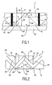
- the filter comprises a first substrate, formed with a plurality of ridges, each having a crest and a base, and a second substrate, formed with a plurality of grooves, said first and second substrate being fitted together, so that said ridges are received by said grooves.
- the two substrates have surfaces with essentially inverse topology. When they are fitted together, the system of beam splitters is created by the surfaces of the grooves and ridges that make contact in the interface between the substrates. The pointed shape is now formed by the bordering surfaces between the substrates, and results from the protrusion between two grooves in the second substrate protruding into a valley between two ridges in the first substrate.
- Fig. 1 shows schematically a part of a filter 1 according to an embodiment of the invention, placed on top of a phosphor layer 10 with A1 backing, forming part of a display unit, e.g. a CRT.
- a contrast enhancement filter can be applied in most displays such as home television and computer monitors. More specifically, it can, in principle, be used in CRTs, plasma displays, "foil" displays, LED displays, etc. Basically it can be used in any display where the light generating medium can be backed by a reflective surface, or is reflective in itself. It can even be used in back-lit LCD displays, although not a lot is to be gained, because an LCD display already absorbs most of the ambient light falling on the display.
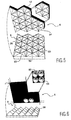
- the pyramids 53 will be three sided, so called retro reflectors.
- the hollows 54 in the top substrate 6 are adapted to receive these pyramids 53.
- the channels 12 would be arranged in a triangular fashion, surrounding each pyramid.
- square pyramids 51 as shown in Fig. 4 may be preferred for square pixels, the retro reflectors have the advantage of being less affected by varying distance to the light source.
Landscapes
- Physics & Mathematics (AREA)
- General Physics & Mathematics (AREA)
- Optics & Photonics (AREA)
- Spectroscopy & Molecular Physics (AREA)
- Devices For Indicating Variable Information By Combining Individual Elements (AREA)
- Optical Elements Other Than Lenses (AREA)
Claims (17)
- Kontraststeigerungsfilter für eine Wiedergabeanordnung mit einem Element mit einer Anzahl verbundener geneigter Oberflächen, die wie eine Anzahl Bündelspalter (2, 4) wirksam sind, so dass Paare aneinander grenzender Bündelspalter (2, 4) spitze Oberflächen bilden, die nach einer ersten Seite (23) des Elementes zeigen, welche die Seite ist, auf die das Umgebungslicht auftrifft, und wobei das Filter eine Anzahl Lichtabsorber (12, 13) aufweist, dadurch gekennzeichnet, dass jeder Lichtabsorber (12, 13) in einem Gebiet (20, 26) zwischen aneinander grenzenden spitzen Oberflächen vorgesehen ist und sich von der genannten ersten Seite (23) des Elementes in Richtung von wenigstens einem der genannten angrenzenden Bündelspaltern (2, 4) erstreckt zum Absorbieren von Licht, das in das genannten Gebiet (20, 26) eintrifft und durch einen der genannten angrenzenden Bündelspalter (2, 4) in Richtung des Lichtabsorbers (12, 13) reflektiert wird.
- Kontraststeigerungsfilter nach Anspruch 1, wobei die genannten Bündelspalter je einen Winkel von 45 Grad mit einer Außenfläche des Filters einschließt.
- Kontraststeigerungsfilter nach Anspruch 1 oder 2, wobei das genannte Element ein Substrat (8) aufweist, das mit einer Anzahl Rillen (26) versehen ist und wobei die genannten Absorber in den genannten Rillen (26) vorgesehen sind.
- Kontraststeigerungsfilter nach Anspruch 1 oder 2, wobei das genannte Element ein Substrat (6) aufweist, das mit einer Anzahl Rippen (20) versehen ist, die je einen Rücken (22) und eine Basis (23) haben und wobei die genannten Absorber durch eine Anzahl Kanäle (12, 13) gebildet werden, die längs der Länge der genannten Rippen (20, 21) gebildet werden, wobei jeder Kanal sich von dem Rücken (22) einer Rippe um einen Abstand in das genannte erste Substrat erstreckt, wobei die genannten Kanäle mit einem das Licht absorbierenden Material (14) gefüllt ist.
- Kontraststeigerungsfilter nach Anspruch 1 oder 2, wobei das genannte Element Folgendes umfasst:- ein erstes Substrat (6), das mit einer Anzahl Rippen versehen ist (20, 21), die je einen Rücken (22) und eine Basis (23) haben, und- ein zweites Substrat (8), das mit einer Anzahl Rillen (26) versehen ist, wobei das genannte erste und zweite Substrat aneinander befestigt werden, so dass die genannten Rippen (20) in die genannten Rillen (26) fallen.
- Kontraststeigerungsfilter nach Anspruch 5, wobei die genannten Absorber durch eine Anzahl Kanäle (12; 13) gebildet werden, die in dem genannten Substrat längs der Länge der genannten Rippen gebildet sind, wobei jeder Kanal sich von dem Rücken (22) einer Rippe über einen Abstand in das erste Substrat erstreckt, wobei die genannten Kanäle mit einem das Licht absorbierenden Material (14) gefüllt werden.
- Kontraststeigerungsfilter nach Anspruch 5 oder 6, wobei das erste Substrat (6) mit parallelen A-förmigen Rippen (20) versehen ist.
- Kontraststeigerungsfilter nach einem der Ansprüche 5 - 7, wobei das zweite Substrat (8) mit parallelen V-förmigen Rillen (26) versehen ist.
- Kontraststeigerungsfilter nach Anspruch 8, wobei das zweite Substrat (8) mit zwei orthogonalen Sätzen paralleler V-förmiger Rillen (26, 30) versehen ist, wobei vorspringende Pyramiden (51) zwischen die genannten Rillen eingelassen werden.
- Kontraststeigerungsfilter nach Anspruch 8, wobei das zweite Substrat (8) mit drei Sätzen paralleler V-förmiger Rillen (26, 50, 55) versehen ist, wobei vorspringende Pyramiden (53) zwischen die genannten Rillen eingelassen werden.
- Kontraststeigerungsfilter nach Anspruch 9 oder 10, wobei die genannten Rippen (20, 21) ein Gitter bilden, mit Hohlräumen (52, 54) zum Empfangen der genannten Pyramiden (51, 53).
- Kontraststeigerungsfilter nach Anspruch 6, wobei das zweite Substrat (8) mit vorspringenden kegelförmigen Formen (56) versehen ist.
- Kontraststeigerungsfilter nach Anspruch 12, wobei das erste Substrat (6) mit Hohlräumen (58) versehen ist zum Empfangen der genannten kegelförmigen Formen (56).
- Kontraststeigerungsfilter nach Anspruch 4, 6 - 13, wobei die genannten Kanäle (12, 13) sich in das Substrat erstrecken, und zwar wenigstens bis an die Basis der genannten Rippen.
- Kontraststeigerungsfilter nach einem der Ansprüche 3-14, wobei wenigstens eines der genannten Substrate (6, 8) mit einer lichtbrechenden Deckschicht bedeckt ist.
- Kontraststeigerungsfilter nach Anspruch 3 - 15, wobei wenigstens eines der genannten Substrate (6, 8) mit einer reflektierenden Deckschicht bedeckt ist.
- Wiedergabeanordnung mit einem Kontraststeigerungsfilter nach einem der vorstehenden Ansprüche.
Priority Applications (1)
| Application Number | Priority Date | Filing Date | Title |
|---|---|---|---|
| EP02777632A EP1449016B1 (de) | 2001-11-12 | 2002-10-22 | Filter zur kontraststeigerung und diesen filter verwendendes anzeigegerät |
Applications Claiming Priority (4)
| Application Number | Priority Date | Filing Date | Title |
|---|---|---|---|
| EP01204301 | 2001-11-12 | ||
| EP01204301 | 2001-11-12 | ||
| PCT/IB2002/004410 WO2003042726A1 (en) | 2001-11-12 | 2002-10-22 | Contrast enhancement filter and display provided with such filter |
| EP02777632A EP1449016B1 (de) | 2001-11-12 | 2002-10-22 | Filter zur kontraststeigerung und diesen filter verwendendes anzeigegerät |
Publications (2)
| Publication Number | Publication Date |
|---|---|
| EP1449016A1 EP1449016A1 (de) | 2004-08-25 |
| EP1449016B1 true EP1449016B1 (de) | 2007-06-06 |
Family
ID=8181214
Family Applications (1)
| Application Number | Title | Priority Date | Filing Date |
|---|---|---|---|
| EP02777632A Expired - Lifetime EP1449016B1 (de) | 2001-11-12 | 2002-10-22 | Filter zur kontraststeigerung und diesen filter verwendendes anzeigegerät |
Country Status (9)
| Country | Link |
|---|---|
| US (1) | US7156529B2 (de) |
| EP (1) | EP1449016B1 (de) |
| JP (1) | JP4361795B2 (de) |
| KR (1) | KR100935834B1 (de) |
| CN (1) | CN100439944C (de) |
| AT (1) | ATE364189T1 (de) |
| DE (1) | DE60220538T2 (de) |
| TW (1) | TWI270694B (de) |
| WO (1) | WO2003042726A1 (de) |
Families Citing this family (15)
| Publication number | Priority date | Publication date | Assignee | Title |
|---|---|---|---|---|
| CN1969206B (zh) * | 2004-06-17 | 2010-09-29 | 皇家飞利浦电子股份有限公司 | 分色滤光器 |
| US7486024B2 (en) * | 2005-11-17 | 2009-02-03 | Lg Electronics Inc. | Display apparatus filter and plasma display apparatus using the same |
| FR2893719A1 (fr) * | 2005-11-24 | 2007-05-25 | Thomson Licensing Sas | Panneau a plasma dote d'un reseau de concentrateurs |
| KR100740227B1 (ko) | 2006-06-15 | 2007-07-18 | 삼성전자주식회사 | 디스플레이 패널 |
| EP1890315A3 (de) | 2006-08-18 | 2009-07-01 | LG Electronics Inc. | Filter und Plasmaanzeigevorrichtung damit |
| US20080042570A1 (en) * | 2006-08-18 | 2008-02-21 | Lg Electronics Inc. | Sheet for protecting external light and plasma display device thereof |
| JP5082752B2 (ja) * | 2006-12-21 | 2012-11-28 | 日亜化学工業株式会社 | 半導体発光素子用基板の製造方法及びそれを用いた半導体発光素子 |
| US7511804B1 (en) * | 2007-04-10 | 2009-03-31 | Itt Manufacturing Enterprises, Inc. | Crossed beam roof target for motion tracking |
| US20090213593A1 (en) * | 2008-02-26 | 2009-08-27 | Reflexite Corporation | Optical device and system for black level enhancement and methods of use thereof |
| US8205995B2 (en) * | 2008-08-07 | 2012-06-26 | Reflexite Corporation | Optical device and system for privacy or contrast enhancement and methods of use thereof |
| US8057715B2 (en) * | 2008-08-28 | 2011-11-15 | Reflexite Corporation | Method for making an optical device and system for privacy or contrast enhancement |
| CN104680947A (zh) * | 2015-02-15 | 2015-06-03 | 北京环宇蓝博科技有限公司 | Led屏幕消除莫尔条纹并提高填充系数的装置及方法 |
| EP3057082B1 (de) | 2015-02-15 | 2019-10-09 | Beijing Universal Lanbo Technology Co., Ltd. | Led-bildschirmabdeckungen und led-anzeigen |
| DE102017205844A1 (de) * | 2017-04-06 | 2018-10-11 | Robert Bosch Gmbh | Lichttransmissionselement, optische Empfangseinheit, optische Aktoreinheit, LiDAR-System, Arbeitsvorrichtung und Fahrzeug |
| JP7516796B2 (ja) * | 2020-03-25 | 2024-07-17 | 大日本印刷株式会社 | 反射型スクリーン、映像表示装置 |
Family Cites Families (9)
| Publication number | Priority date | Publication date | Assignee | Title |
|---|---|---|---|---|
| US2773411A (en) * | 1955-12-30 | 1956-12-11 | Otto G Schwede | Angular discriminating optical device |
| US4070100A (en) * | 1976-09-01 | 1978-01-24 | Katsuyuki Akiyoshi | Filter for partially transmitting light |
| US4165920A (en) * | 1977-07-27 | 1979-08-28 | Qantix Corporation | Echo reduction improvement in a front face glare reduction overlay |
| EP0304517B1 (de) | 1987-08-24 | 1994-11-02 | Qantix Corporation | Blendschutzfilter |
| US4726662A (en) * | 1985-09-24 | 1988-02-23 | Talig Corporation | Display including a prismatic lens system or a prismatic reflective system |
| US5608286A (en) * | 1994-11-30 | 1997-03-04 | Texas Instruments Incorporated | Ambient light absorbing face plate for flat panel display |
| JPH1039418A (ja) * | 1996-07-19 | 1998-02-13 | Kimoto & Co Ltd | 反射型スクリーンおよびその製造方法 |
| US6597417B1 (en) * | 2000-07-25 | 2003-07-22 | Scram Technologies, Inc. | Optical panel having black material between apexes of serrations on the inlet face |
| US6398370B1 (en) * | 2000-11-15 | 2002-06-04 | 3M Innovative Properties Company | Light control device |
-
2002
- 2002-10-22 EP EP02777632A patent/EP1449016B1/de not_active Expired - Lifetime
- 2002-10-22 WO PCT/IB2002/004410 patent/WO2003042726A1/en not_active Ceased
- 2002-10-22 US US10/494,824 patent/US7156529B2/en not_active Expired - Fee Related
- 2002-10-22 KR KR1020047007227A patent/KR100935834B1/ko not_active Expired - Fee Related
- 2002-10-22 JP JP2003544503A patent/JP4361795B2/ja not_active Expired - Fee Related
- 2002-10-22 AT AT02777632T patent/ATE364189T1/de not_active IP Right Cessation
- 2002-10-22 CN CNB028223624A patent/CN100439944C/zh not_active Expired - Fee Related
- 2002-10-22 DE DE60220538T patent/DE60220538T2/de not_active Expired - Lifetime
- 2002-11-01 TW TW091132395A patent/TWI270694B/zh not_active IP Right Cessation
Also Published As
| Publication number | Publication date |
|---|---|
| KR20040063148A (ko) | 2004-07-12 |
| JP2005509895A (ja) | 2005-04-14 |
| TWI270694B (en) | 2007-01-11 |
| CN1585905A (zh) | 2005-02-23 |
| KR100935834B1 (ko) | 2010-01-08 |
| ATE364189T1 (de) | 2007-06-15 |
| CN100439944C (zh) | 2008-12-03 |
| WO2003042726A1 (en) | 2003-05-22 |
| US20040257658A1 (en) | 2004-12-23 |
| JP4361795B2 (ja) | 2009-11-11 |
| DE60220538D1 (de) | 2007-07-19 |
| DE60220538T2 (de) | 2008-01-31 |
| US7156529B2 (en) | 2007-01-02 |
| EP1449016A1 (de) | 2004-08-25 |
| TW200407564A (en) | 2004-05-16 |
Similar Documents
| Publication | Publication Date | Title |
|---|---|---|
| EP1449016B1 (de) | Filter zur kontraststeigerung und diesen filter verwendendes anzeigegerät | |
| US5851062A (en) | Prism sheet for surface light source | |
| AU700859B2 (en) | Liquid crystal display and its manufacturing method | |
| US8107036B2 (en) | Backlight device, liquid crystal display apparatus, and light deflecting sheet | |
| KR100667537B1 (ko) | 액정표시장치의 컬러필터 및 그 제조방법 | |
| US11537004B2 (en) | Transparent display substrate and transparent display device | |
| KR100630284B1 (ko) | 액티브 매트릭스형 표시장치 | |
| US20110255159A1 (en) | Autostereoscopic display device | |
| KR100578772B1 (ko) | 조명장치, 도광체 및 액정표시장치 | |
| US6685343B2 (en) | Light guide plate, and surface light source device and display device utilizing the same | |
| US7712911B2 (en) | Image display device and light diffusion component for use therein | |
| KR20010085356A (ko) | 액정표시장치 | |
| KR100530722B1 (ko) | 액티브 매트릭스형 표시장치 | |
| JP2008145551A (ja) | 表示装置 | |
| JP2006337526A (ja) | 光学フィルム、バックライト装置および液晶表示装置 | |
| CN116300206B (zh) | 显示模组和显示装置 | |
| JP2006100125A (ja) | プリズムレンズフィルム及びこれを用いた平面型発光装置 | |
| JP2021515913A (ja) | 傾斜マルチビームコラムを有する水平視差マルチビューディスプレイ及び方法 | |
| TWI813340B (zh) | 具有不同突出距離的反射式子元件的多視像背光件、顯示器和方法 | |
| JP3899717B2 (ja) | 液晶表示装置 | |
| JP2006098747A (ja) | プリズムレンズフィルム及びこれを用いた平面型発光装置 | |
| KR100756132B1 (ko) | 플라즈마 디스플레이 패널의 콘트라스트 향상 광학 시트,그의 제조 방법 및 그를 이용한 플라즈마 디스플레이 패널 | |
| CN210294705U (zh) | 一种背光源结构 | |
| KR100760096B1 (ko) | 플라즈마 디스플레이 패널의 콘트라스트 향상 광학 시트및 그의 제조 방법 | |
| KR100875491B1 (ko) | 도광판 및 이를 이용한 백라이트 유닛 그리고 액정디스플레이 장치 |
Legal Events
| Date | Code | Title | Description |
|---|---|---|---|
| PUAI | Public reference made under article 153(3) epc to a published international application that has entered the european phase |
Free format text: ORIGINAL CODE: 0009012 |
|
| 17P | Request for examination filed |
Effective date: 20040614 |
|
| AK | Designated contracting states |
Kind code of ref document: A1 Designated state(s): AT BE BG CH CY CZ DE DK EE ES FI FR GB GR IE IT LI LU MC NL PT SE SK TR |
|
| AX | Request for extension of the european patent |
Extension state: AL LT LV MK RO SI |
|
| GRAP | Despatch of communication of intention to grant a patent |
Free format text: ORIGINAL CODE: EPIDOSNIGR1 |
|
| GRAS | Grant fee paid |
Free format text: ORIGINAL CODE: EPIDOSNIGR3 |
|
| GRAA | (expected) grant |
Free format text: ORIGINAL CODE: 0009210 |
|
| AK | Designated contracting states |
Kind code of ref document: B1 Designated state(s): AT BE BG CH CY CZ DE DK EE ES FI FR GB GR IE IT LI LU MC NL PT SE SK TR |
|
| PG25 | Lapsed in a contracting state [announced via postgrant information from national office to epo] |
Ref country code: FI Free format text: LAPSE BECAUSE OF FAILURE TO SUBMIT A TRANSLATION OF THE DESCRIPTION OR TO PAY THE FEE WITHIN THE PRESCRIBED TIME-LIMIT Effective date: 20070606 Ref country code: CH Free format text: LAPSE BECAUSE OF FAILURE TO SUBMIT A TRANSLATION OF THE DESCRIPTION OR TO PAY THE FEE WITHIN THE PRESCRIBED TIME-LIMIT Effective date: 20070606 Ref country code: LI Free format text: LAPSE BECAUSE OF FAILURE TO SUBMIT A TRANSLATION OF THE DESCRIPTION OR TO PAY THE FEE WITHIN THE PRESCRIBED TIME-LIMIT Effective date: 20070606 |
|
| REG | Reference to a national code |
Ref country code: GB Ref legal event code: FG4D |
|
| REG | Reference to a national code |
Ref country code: CH Ref legal event code: EP |
|
| REG | Reference to a national code |
Ref country code: IE Ref legal event code: FG4D |
|
| REF | Corresponds to: |
Ref document number: 60220538 Country of ref document: DE Date of ref document: 20070719 Kind code of ref document: P |
|
| PG25 | Lapsed in a contracting state [announced via postgrant information from national office to epo] |
Ref country code: SE Free format text: LAPSE BECAUSE OF FAILURE TO SUBMIT A TRANSLATION OF THE DESCRIPTION OR TO PAY THE FEE WITHIN THE PRESCRIBED TIME-LIMIT Effective date: 20070906 |
|
| PG25 | Lapsed in a contracting state [announced via postgrant information from national office to epo] |
Ref country code: ES Free format text: LAPSE BECAUSE OF FAILURE TO SUBMIT A TRANSLATION OF THE DESCRIPTION OR TO PAY THE FEE WITHIN THE PRESCRIBED TIME-LIMIT Effective date: 20070917 |
|
| PG25 | Lapsed in a contracting state [announced via postgrant information from national office to epo] |
Ref country code: AT Free format text: LAPSE BECAUSE OF FAILURE TO SUBMIT A TRANSLATION OF THE DESCRIPTION OR TO PAY THE FEE WITHIN THE PRESCRIBED TIME-LIMIT Effective date: 20070606 |
|
| ET | Fr: translation filed | ||
| NLV1 | Nl: lapsed or annulled due to failure to fulfill the requirements of art. 29p and 29m of the patents act | ||
| REG | Reference to a national code |
Ref country code: CH Ref legal event code: PL |
|
| PG25 | Lapsed in a contracting state [announced via postgrant information from national office to epo] |
Ref country code: BE Free format text: LAPSE BECAUSE OF FAILURE TO SUBMIT A TRANSLATION OF THE DESCRIPTION OR TO PAY THE FEE WITHIN THE PRESCRIBED TIME-LIMIT Effective date: 20070606 |
|
| PG25 | Lapsed in a contracting state [announced via postgrant information from national office to epo] |
Ref country code: CZ Free format text: LAPSE BECAUSE OF FAILURE TO SUBMIT A TRANSLATION OF THE DESCRIPTION OR TO PAY THE FEE WITHIN THE PRESCRIBED TIME-LIMIT Effective date: 20070606 Ref country code: NL Free format text: LAPSE BECAUSE OF FAILURE TO SUBMIT A TRANSLATION OF THE DESCRIPTION OR TO PAY THE FEE WITHIN THE PRESCRIBED TIME-LIMIT Effective date: 20070606 Ref country code: PT Free format text: LAPSE BECAUSE OF FAILURE TO SUBMIT A TRANSLATION OF THE DESCRIPTION OR TO PAY THE FEE WITHIN THE PRESCRIBED TIME-LIMIT Effective date: 20071106 Ref country code: BG Free format text: LAPSE BECAUSE OF FAILURE TO SUBMIT A TRANSLATION OF THE DESCRIPTION OR TO PAY THE FEE WITHIN THE PRESCRIBED TIME-LIMIT Effective date: 20070906 |
|
| PG25 | Lapsed in a contracting state [announced via postgrant information from national office to epo] |
Ref country code: SK Free format text: LAPSE BECAUSE OF FAILURE TO SUBMIT A TRANSLATION OF THE DESCRIPTION OR TO PAY THE FEE WITHIN THE PRESCRIBED TIME-LIMIT Effective date: 20070606 |
|
| PLBE | No opposition filed within time limit |
Free format text: ORIGINAL CODE: 0009261 |
|
| STAA | Information on the status of an ep patent application or granted ep patent |
Free format text: STATUS: NO OPPOSITION FILED WITHIN TIME LIMIT |
|
| PG25 | Lapsed in a contracting state [announced via postgrant information from national office to epo] |
Ref country code: DK Free format text: LAPSE BECAUSE OF FAILURE TO SUBMIT A TRANSLATION OF THE DESCRIPTION OR TO PAY THE FEE WITHIN THE PRESCRIBED TIME-LIMIT Effective date: 20070606 Ref country code: GR Free format text: LAPSE BECAUSE OF FAILURE TO SUBMIT A TRANSLATION OF THE DESCRIPTION OR TO PAY THE FEE WITHIN THE PRESCRIBED TIME-LIMIT Effective date: 20070907 Ref country code: IT Free format text: LAPSE BECAUSE OF FAILURE TO SUBMIT A TRANSLATION OF THE DESCRIPTION OR TO PAY THE FEE WITHIN THE PRESCRIBED TIME-LIMIT Effective date: 20070606 |
|
| 26N | No opposition filed |
Effective date: 20080307 |
|
| PG25 | Lapsed in a contracting state [announced via postgrant information from national office to epo] |
Ref country code: MC Free format text: LAPSE BECAUSE OF NON-PAYMENT OF DUE FEES Effective date: 20071031 |
|
| PG25 | Lapsed in a contracting state [announced via postgrant information from national office to epo] |
Ref country code: IE Free format text: LAPSE BECAUSE OF NON-PAYMENT OF DUE FEES Effective date: 20071022 |
|
| PG25 | Lapsed in a contracting state [announced via postgrant information from national office to epo] |
Ref country code: EE Free format text: LAPSE BECAUSE OF FAILURE TO SUBMIT A TRANSLATION OF THE DESCRIPTION OR TO PAY THE FEE WITHIN THE PRESCRIBED TIME-LIMIT Effective date: 20070606 |
|
| PG25 | Lapsed in a contracting state [announced via postgrant information from national office to epo] |
Ref country code: CY Free format text: LAPSE BECAUSE OF FAILURE TO SUBMIT A TRANSLATION OF THE DESCRIPTION OR TO PAY THE FEE WITHIN THE PRESCRIBED TIME-LIMIT Effective date: 20070606 |
|
| PG25 | Lapsed in a contracting state [announced via postgrant information from national office to epo] |
Ref country code: LU Free format text: LAPSE BECAUSE OF NON-PAYMENT OF DUE FEES Effective date: 20071022 |
|
| PG25 | Lapsed in a contracting state [announced via postgrant information from national office to epo] |
Ref country code: TR Free format text: LAPSE BECAUSE OF FAILURE TO SUBMIT A TRANSLATION OF THE DESCRIPTION OR TO PAY THE FEE WITHIN THE PRESCRIBED TIME-LIMIT Effective date: 20070606 |
|
| REG | Reference to a national code |
Ref country code: GB Ref legal event code: 732E Free format text: REGISTERED BETWEEN 20120906 AND 20120912 |
|
| REG | Reference to a national code |
Ref country code: FR Ref legal event code: TP Owner name: TP VISION HOLDING B.V., NL Effective date: 20121022 |
|
| REG | Reference to a national code |
Ref country code: DE Ref legal event code: R082 Ref document number: 60220538 Country of ref document: DE Representative=s name: VOLMER, GEORG, DIPL.-ING., DE |
|
| REG | Reference to a national code |
Ref country code: DE Ref legal event code: R082 Ref document number: 60220538 Country of ref document: DE Representative=s name: VOLMER, GEORG, DIPL.-ING., DE Effective date: 20130130 Ref country code: DE Ref legal event code: R081 Ref document number: 60220538 Country of ref document: DE Owner name: TP VISION HOLDING B.V., NL Free format text: FORMER OWNER: KONINKLIJKE PHILIPS ELECTRONICS N.V., EINDHOVEN, NL Effective date: 20130130 |
|
| PGFP | Annual fee paid to national office [announced via postgrant information from national office to epo] |
Ref country code: FR Payment date: 20131031 Year of fee payment: 12 Ref country code: GB Payment date: 20131031 Year of fee payment: 12 |
|
| PGFP | Annual fee paid to national office [announced via postgrant information from national office to epo] |
Ref country code: DE Payment date: 20131230 Year of fee payment: 12 |
|
| REG | Reference to a national code |
Ref country code: DE Ref legal event code: R119 Ref document number: 60220538 Country of ref document: DE |
|
| GBPC | Gb: european patent ceased through non-payment of renewal fee |
Effective date: 20141022 |
|
| PG25 | Lapsed in a contracting state [announced via postgrant information from national office to epo] |
Ref country code: GB Free format text: LAPSE BECAUSE OF NON-PAYMENT OF DUE FEES Effective date: 20141022 Ref country code: DE Free format text: LAPSE BECAUSE OF NON-PAYMENT OF DUE FEES Effective date: 20150501 |
|
| REG | Reference to a national code |
Ref country code: FR Ref legal event code: ST Effective date: 20150630 |
|
| PG25 | Lapsed in a contracting state [announced via postgrant information from national office to epo] |
Ref country code: FR Free format text: LAPSE BECAUSE OF NON-PAYMENT OF DUE FEES Effective date: 20141031 |