EP1450433B1 - Schaltungsanordnung zur Unterdrückung von parasitären Wellentypen auf planaren Wellenleitern - Google Patents
Schaltungsanordnung zur Unterdrückung von parasitären Wellentypen auf planaren Wellenleitern Download PDFInfo
- Publication number
- EP1450433B1 EP1450433B1 EP04012771A EP04012771A EP1450433B1 EP 1450433 B1 EP1450433 B1 EP 1450433B1 EP 04012771 A EP04012771 A EP 04012771A EP 04012771 A EP04012771 A EP 04012771A EP 1450433 B1 EP1450433 B1 EP 1450433B1
- Authority
- EP
- European Patent Office
- Prior art keywords
- circuit
- port
- transmission line
- spurious mode
- mode wave
- Prior art date
- Legal status (The legal status is an assumption and is not a legal conclusion. Google has not performed a legal analysis and makes no representation as to the accuracy of the status listed.)
- Expired - Lifetime
Links
- 230000005540 biological transmission Effects 0.000 title claims description 78
- 230000001629 suppression Effects 0.000 title description 2
- 239000004020 conductor Substances 0.000 claims description 52
- 238000004891 communication Methods 0.000 claims description 15
- 230000001902 propagating effect Effects 0.000 claims description 6
- 230000008878 coupling Effects 0.000 claims description 5
- 238000010168 coupling process Methods 0.000 claims description 5
- 238000005859 coupling reaction Methods 0.000 claims description 5
- 238000012545 processing Methods 0.000 claims description 3
- 230000005284 excitation Effects 0.000 description 8
- 230000015572 biosynthetic process Effects 0.000 description 7
- 238000005520 cutting process Methods 0.000 description 7
- 238000010586 diagram Methods 0.000 description 7
- 230000005672 electromagnetic field Effects 0.000 description 7
- 230000000644 propagated effect Effects 0.000 description 7
- 230000000903 blocking effect Effects 0.000 description 5
- 238000009826 distribution Methods 0.000 description 3
- 230000005684 electric field Effects 0.000 description 3
- 238000000059 patterning Methods 0.000 description 3
- 239000003990 capacitor Substances 0.000 description 2
- 230000008859 change Effects 0.000 description 2
- 239000011159 matrix material Substances 0.000 description 2
- 238000000034 method Methods 0.000 description 2
- 230000004048 modification Effects 0.000 description 2
- 238000012986 modification Methods 0.000 description 2
- 230000003071 parasitic effect Effects 0.000 description 2
- 238000004088 simulation Methods 0.000 description 2
- 239000000758 substrate Substances 0.000 description 2
- 239000010409 thin film Substances 0.000 description 2
- 239000013598 vector Substances 0.000 description 2
- 230000000052 comparative effect Effects 0.000 description 1
- 238000013461 design Methods 0.000 description 1
- 230000000694 effects Effects 0.000 description 1
- 230000008030 elimination Effects 0.000 description 1
- 238000003379 elimination reaction Methods 0.000 description 1
- 238000004519 manufacturing process Methods 0.000 description 1
- 230000007246 mechanism Effects 0.000 description 1
- 230000010355 oscillation Effects 0.000 description 1
- 238000012856 packing Methods 0.000 description 1
- 230000002093 peripheral effect Effects 0.000 description 1
Images















Classifications
-
- H—ELECTRICITY
- H01—ELECTRIC ELEMENTS
- H01P—WAVEGUIDES; RESONATORS, LINES, OR OTHER DEVICES OF THE WAVEGUIDE TYPE
- H01P3/00—Waveguides; Transmission lines of the waveguide type
-
- H—ELECTRICITY
- H01—ELECTRIC ELEMENTS
- H01P—WAVEGUIDES; RESONATORS, LINES, OR OTHER DEVICES OF THE WAVEGUIDE TYPE
- H01P1/00—Auxiliary devices
- H01P1/16—Auxiliary devices for mode selection, e.g. mode suppression or mode promotion; for mode conversion
Definitions
- the present invention relates to a high frequency circuit device such as a waveguide, a resonator, or the like including two parallel plane conductors, and a communication device using the high frequency circuit device.
- transmission lines for use in a microwave or millimeter-wave band different types are employed, such as grounded coplanar transmission lines each containing a dielectric plate having a ground electrode formed substantially on the whole of one face thereof and a coplanar line formed on the other face thereof; grounded slot transmission lines each containing a dielectric plate having a grounded electrode formed on one face thereof and a slot formed on the other face thereof; planar dielectric transmission lines each containing a dielectric plate having slots formed on both of the faces of the dielectric plate, in opposition to each other through the dielectric plate, and so forth.
- All of these transmission lines are formed so as to contain two parallel plane conductors. Therefore, there has arisen the problem that if an electromagnetic field is disturbed in input-output portions and bends of the transmission lines, a spurious mode wave such as a so-called parallel plate mode wave or the like is excited between the two parallel plane conductors, and the spurious mode wave is propagated between the plane conductors. In some cases, problematically, interference is caused by the spurious mode leakage wave between the adjacent transmission lines, so that a signal leaks between the lines, and so forth.
- FIG. 42 shows an example of the principal propagation mode of a grounded coplanar transmission line and a parallel mode electromagnetic field distribution generated incidentally to the principal propagation mode.
- an electrode 21 is formed substantially on the whole of the lower face of a dielectric plate 20, and a strip conductor 19 and an electrode 22 are formed on the upper face thereof.
- the electrodes 21 and 22 are used as ground electrodes.
- These electrodes, the dielectric plate 20, and the strip conductor 19 constitute a grounded coplanar transmission line.
- through-holes electrically connecting electrodes formed on the upper and lower faces of a dielectric plate are provided along a transmission line, on both of the sides thereof and at intervals sufficiently short with respect to the propagation mode wavelength.
- the through-hole parts act as electrical walls, where propagation of the parallel plate mode wave is prevented.
- a high frequency range such as a millimeter wave band or the like
- the applicant of the present invention has filed Japanese Patent Application No. 11-025873 on a spurious mode wave propagation blocking circuit in which inductors and capacitors are combined to form a lumped-constant circuit and are arranged in a two dimensional form.
- EP 0 975 043 A2 discloses a high-frequency circuit device and communication apparatus, wherein electrodes are formed on both top and bottom surfaces of a dielectric plate and grounded coplanar lines, as transmission lines, are formed on the top surface of the dielectric plate.
- a plurality of micro-strip lines, each composed of high-impedance lines and low-impedance lines alternately connected in series, is arranged at a pitch shorter than the wavelength of a wave traveling along the grounded coplanar lines.
- a spurious mode propagation-blocking surface thus constructed prevents a spurious mode wave, such as a parallel-plate mode, from traveling.
- a high frequency circuit device which comprises at least two parallel plane conductors, a circuit for exciting an electromagnetic wave, provided between the two plane conductors, and a spurious mode wave propagation-blocking circuit for coupling to a spurious mode wave propagating between the two plane conductors to block the propagation of the spurious mode wave, formed on either or both of the two plane conductors, the spurious mode wave propagation-blocking circuit comprising a plurality of arranged fundamental patterns each made of a strip conductor and constituting a multi-port circuit having at least two ports, the strip conductor and constituting a multi-port circuit having at least two ports, the strip conductor of the two-port circuit being determined so that any arbitrary two-port circuit of the respective fundamental patterns has a band-stop filter characteristic.
- a strip transmission line with an open end, having an electrical length equal to 1/4 wavelength at a service frequency is connected in parallel to a strip conductor of the two-port circuit, e.g., as shown in FIG. 1.
- a strip conductor of the two-port circuit e.g., as shown in FIG. 1.
- the above-described high frequency circuit device is used as a communication signal propagation section or a communication signal processing section, in combination with transmitting and/or receiving circuits.
- the total reflection condition of a four-port circuit as an example of a circuit pattern for use in a spurious suppression mechanism is determined based on a characteristic value theory by using the periodicity of the circuit pattern and moreover, the condition that an input wave is totally reflected.
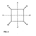
- an arbitrary four-port circuit is simply expressed as in FIG. 2. Assuming that there is no loss in the circuit, the unitary condition is valid.
- the respective parameters of S 11 , S 12 , S 13 , S 14 , S 21 , S 22 , S 23 .... S 42 , S 43 , S 44 can be reduced to the four parameters, that is, S 11 to S 41 .
- the symmetric condition of the circuit is applied to this scattering matrix.
- the whole of the four-port circuit can be analyzed by analysis of the one-port circuits in which even excitation or odd excitation occurs on the two symmetric planes, respectively.
- even excitation hereinafter, referred to as even, briefly
- odd excitation hereinafter, referred to as odd, briefly
- the one-port circuits formed by cutting the four-port circuit along the symmetric axes shown in FIG. 2 correspond to the above-described four conditions (1) to (4), respectively.
- (V) means voltage
- + 1(V) and - 1(V) mean that the voltages have opposite polarities.
- the contents of Table I show the characteristic vectors corresponding to the above conditions (1) to (4), respectively.
- the corresponding characteristic values can be defined. If the characteristic reflection coefficients corresponding to the conditions (1) to (4) are represented by S 11 ee , S 11 eo , S 11 oe , and S 11 oo , the S parameters of the whole of the circuit, that is, S 11 , S 21 , S 31 , and S 41 are expressed by the following formulae.
- S 11 S 11 oe + S 11 oo + S 11 oe + S 11 oo / 4
- S 21 S 11 ee + S 11 eo - S 11 oe - S 11 oo / 4
- S 31 S 11 ee - S 11 eo - S 11 oe + S 11 oo / 4
- S 41 S 11 ee - S 11 eo + S 11 oo - S 11 oo / 4
- Condition 2 can be obtained, namely that the 1/8 circuits formed by cutting along the symmetric planes have the same impedance, irrespective of whether the symmetric planes are open or short-circuited.
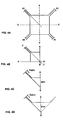
- FIGS. 4A to 4D illustrate the above two conditions.
- the 1/4 circuit part of FIG. 4B is obtained by cutting the pattern of FIG. 4A in quarters.
- the circuit part of FIG. 4B is symmetric about the center line C-C'.
- the impedance Z open seen from the port when the symmetric plane is open, is equal to the impedance Z short of the 1/8 circuit shown in FIG. 4D, seen from the port when the symmetric plane is short-circuited.
- the total reflection condition of the four-port circuit of which the symmetry of the circuit is assumed is valid in the case of three or more-port circuits.
- the basis of the validity will be described.
- FIG. 5A shows a symmetric two-port circuit to demonstrate that the above-described condition 2 is coincident with the total reflection condition of a two-port circuit.
- FIGS. 5B and 5C show two equivalent circuits of the one-port circuit formed by cutting along the symmetric plane shown in FIG. 5A, obtained when the respective symmetric planes are open or short-circuited.
- S 11 and S 21 of the equivalent circuit shown in FIG. 5A are expressed as follows.
- S 11 S 11 e + S 11 o / 2
- S 21 S 11 e - S 11 o / 2
- the total reflection condition of a two-port circuit is that the one-port circuits formed by cutting along the symmetric plane have an equal impedance, irrespective of whether the symmetric planes are open or short-circuited.
- the total reflection condition can be satisfied between arbitrary two-port circuits in a multi-port circuit, the total reflection condition of the whole of the multi-port circuit can be satisfied, as seen in the above description.
- FIG. 17 shows the equivalent circuit in which the simulation was made.
- FIG. 18 shows examples of the characteristics of S 11 , S 21 , S 31 , and S 41 in the above-described circuit. A large reflection coefficient can be obtained over a wide band even in the asymmetrical circuit, as seen in the characteristic of S 11 shown in FIG. 18.
- FIGS. 6A to 6B fundamental patterns shown in FIGS. 6A to 6B can be formed.
- the example of FIG. 6A is a three-port circuit, that of FIG. 6B is a five-port circuit, and that of FIG. 6C is a six-port circuit.
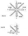
- FIG. 7B shows an example of one-port circuit satisfying the conditions 1 and 2. That is, FIG. 7B shows the one-port circuit formed by cutting the circuit of FIG. 7A along the two symmetric planes A-A' and B-B'.
- the one-port circuit has the configuration in which two 1/4 wavelength stubs having an open terminal are connected to the transmission line connected to a port #1, respectively.
- the impedances of the two stubs are changed, depending on the state, in which the two symmetric planes are open or short-circuited.
- FIGS. 8A to 8B show equivalent circuits corresponding to the state of the two symmetric planes.
- FIG. 8A, 8B, 8C, and 8D show the states wherein the plane A-A' is open, and the plane B-B' is open; wherein the plane A-A' is open, and the plane B-B' is short-circuited; wherein the plane A-A' is short-circuited, and the plane B-B' is open, and that the plane A-A' is short-circuited, and the plane B-B' is short-circuited, respectively.
- the circuits are equivalent to the circuits in which no stub exists when a symmetric plane is short-circuited, respectively.
- the mode present in the stub is assumed to be is only a TEM mode, and furthermore, it is presumed that the waves in the TE01 and TE03 modes in which the symmetric planes are open are evanescent waves, and effects of the waves are estimated to be extremely small.
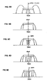
- the mode of a wave propagating in a strip conductor such modes as shown in FIGS. 9A-9E are exemplified. These modes correspond to elimination of the presence condition of the TEM wave, TE02, and TE04 modes wherein the symmetric plane is assumed to be a short-circuit plane.
- the mode present in the stub is only the TEM wave mode.
- FIG. 10 shows a modification example of the fundamental pattern shown in FIG. 7A.
- the respective stubs shown in FIG. 7A have a meandering shape so that the whole of the fundamental pattern is formed within a square area.
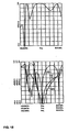
- FIGS. 11A and 11B show the S parameters of the circuit of FIG. 10.
- the optimum frequency is set at 32 GHz. That is, at 32 GHz, the electrical length of the stub becomes 1/4 wavelength. For this reason, the total reflection characteristic is presented over a predetermined band having this frequency at the center.
- FIGS. 12A and 12B show the case in which the application frequency is set at 20 GHz in the pattern of FIG. 10.
- the electrical length of the stub becomes 1/4 wavelength at 20 GHz. For this reason, the total reflection characteristic is presented in a band having this frequency as the center.
- FIG. 13 shows a pattern as a comparative example, shown in Japanese Patent Application No. 11-025874 .
- FIGS. 14A and 14B show the frequency characteristics of the S parameters.
- the designed frequency band is set to be 32 GHz, as in the cases of FIGS. 10, 11A, and 11B, one side of the square fundamental pattern has a length of 0.8 mm in the example of FIG. 13, while one side of the square pattern has a length of 0.25 mm in the example of FIG. 10.
- the example of FIG. 10 is very small in size, and the reflection characteristic is excellent. It can be seen that the propagation blocking ability for a spurious mode wave is very high.
- FIG. 15 shows an example of another fundamental pattern.
- This fundamental pattern is formed by connecting 1/4 wavelength transmission lines in series with the input-output ports of the pattern of FIG. 10.
- FIG. 16 shows the frequency characteristics of the S parameters. Like this, by adding the transmission lines each having predetermined impedance and electrical length, the bandwidth can be increased.
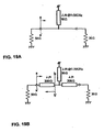
- FIG. 19A shows a fundamental two-port circuit.
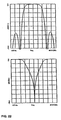
- the circuit has the reflection characteristic shown in FIG. 20.
- a 1/4 wavelength high impedance transmission line is added to the circuit of FIG. 19A to form a circuit as shown in FIG. 19B, the characteristic can be presented with a wide band width as shown in FIG. 22.
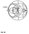
- the physical meaning of the characteristic presented with a wide band width will be described by use of Smith charts.
- the locus of the impedance As regards the locus of the impedance, as viewed from the broken line a-a', obtained when a 1/4 wavelength high impedance transmission line is connected to the circuit shown in FIG. 19A to form the circuit shown in FIG. 19B, and the frequency is changed from 1.0 GHz to 60.0 GHz, the reflection coefficient at 30 GHz, positioned at point A in FIG. 21 is shifted to point B, as shown in FIG. 23.
- the high impedance transmission line enhances the standardized apparent impedance, viewed from line b - b', so that the whole of the characteristic is shifted to the right-hand side (in the direction indicated by the arrow in FIG. 23).
- the change of the imaginary part in the Smith chart is small on the open side and is large on the short side.
- FIG. 24 shows an example in which, in addition, 90° phase shifters are added to the input and output of the circuit shown in FIG. 19B, so that the input-output impedance becomes a low impedance.
- the band-width of the reflection characteristic of this circuit is increased as shown in FIG. 25.
- the locus of the impedance as viewed from the broken line a - a', obtained when the frequency is changed from 1.0 GHz to 60.00 GHz, makes a round figure in the Smith chart, as shown in Fig. 26.
- the whole of the characteristic is shifted toward the left side, due to the low impedance transmission line.
- the resonance loop (impedance locus) originally drawn in the left direction is wholly pushed in the outer peripheral direction of the circle.
- the wide band width can be realized.
- a bandwidth can be increased by adding a transmission line having an appropriate impedance and an adequate electrical length to an input and to an output.
- FIGS. 7A, 10, 15, and so forth show examples based on a four-port circuit.
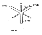
- the present invention can be applied to a three-port circuit as shown in FIG. 27, and moreover, can be applied to a multi-port circuit having at least five ports.
- FIGS. 28A and 28B show examples of another fundamental pattern satisfying the above-described total reflection condition.
- a 1/4 wavelength stub having an open end is provided for a strip conductor connecting two adjacent ports, as shown in FIG. 28A, which is formed from the state shown in FIG. 7A via the state shown in FIG. 28B.
- the length of the strip conductors connecting the two ports and the connection positions of the stubs to the strip conductors have no relation to the above-described total reflection condition.
- FIGS. 7A and 7B are expressed in the form of equivalent circuits, and are simplified.
- FIGS. 30A, 30B and 30C show examples of the fundamental patterns having the same characteristics as the obtained equivalent circuit patterns.
- FIG. 30A shows the equivalent circuit of the pattern shown in FIG. 7A.
- FIG. 30B shows the equivalent circuit obtained by simplifying the pattern.
- FIG. 30C shows a concrete circuit example of the equivalent circuit of FIG. 31B.
- a stub is provided between the ports #2 and #3. Electrically, the circuit pattern has the structure in which the stub is connected in parallel to the strip conductor connecting the two ports.
- the circuit pattern has the structure in which the stubs are connected near to the crossing point of the four ports, and therefore, between any two of the ports, that is, between the ports #1 and #2, between the ports #2 and #3, between the ports #3 and #4, between the ports #4 and #1, between the ports #1 and #3, or between the ports #2 and #4, a stub is connected in parallel to the strip conductor connecting the two ports.
- the above-described stubs are strip transmission lines each having an electrical length of 1/4 wavelength and having an open end. Accordingly, the present invention includes the structure in which a band-stop single stub is connected to a strip conductor connecting at least two ports, as described above.
- FIG. 21 shows a spurious mode wave propagation blocking circuit pattern comprising a plurality of the fundamental patterns each shown in FIG. 30C and arranged in the longitudinal and transverse directions.
- the port #1 is connected to the port #3 of a neighboring fundamental pattern
- the port #2 is connected to the port #4 of another neighboring fundamental pattern.
- FIGS. 32A and 32B show an example of another simplified pattern obtained from the equivalent circuit shown in FIG. 30A as a starting equivalent circuit.
- the equivalent circuit shown in FIG. 32A two stubs each having an open end with a length of 1/4 wavelength are provided for a strip conductor connecting two ports.
- FIG. 32B is a concrete circuit pattern.
- the ports # 1 is connected to the port #3 of a neighboring pattern, and the port #2 is connected to the port #4 of another neighboring pattern.
- FIGS. 33A and 33B show a concrete example of a three-port circuit.
- FIG. 33A shows the fundamental pattern. In this pattern, the respective stubs as shown in FIG. 27 are formed into a meander shape.
- FIG. 33B shows that the fundamental patterns of FIG. 33A are arranged in a two dimensional plane shape, and the three ports are connected in common to each other, correspondingly.
- the profile of the fundamental pattern is triangular. Accordingly, in the case in which a spurious mode wave propagation-blocking circuit is formed in a space sandwiched between two transmission lines or electrode patterns, and the angle between the two transmission lines or electrode patterns is 60° or an angle near to 60°, the fundamental patterns can be arranged at a high packing ratio.
- FIG. 34 is a perspective view of a high frequency circuit device provided with a slot transmission line.
- electrodes 21 and 22 are formed on the under and upper faces of a dielectric plate 20, respectively, and a slot is formed in a predetermined position, whereby a grounded slot transmission line 4 is formed.
- Spurious mode wave propagation-blocking circuits 3 as shown in FIG. 31 or one of the other figures, are formed on both sides of the slot transmission line. In FIG. 34, the spurious mode wave propagation-blocking circuits 3 are shown in a simplified form.
- spurious mode wave propagation-blocking circuits 3 are provided on both sides of the slot transmission line and along the slot transmission line, parallel plate mode waves, generated by coupling to the slot mode wave, are converted to the microstrip transmission line mode waves of the spurious mode wave propagation-blocking circuits and totally reflected. Thereby, on the outside of the respective spurious mode wave propagation-blocking circuits 3, substantially no parallel plate mode waves are propagated. Thus, no undesired coupling to adjacent transmission line waves occurs.
- the spurious mode wave propagation-blocking circuits are formed in the electrode having the slot formed therein.
- the spurious mode wave propagation-blocking circuits 3 may be formed on the ground electrode 21 side.
- the spurious mode wave propagation-blocking circuits may be provided in both the ground electrode 21 and the electrode 22 in which the slot is formed.
- the ground electrode 21 is formed on the under face of the dielectric plate 20, and the electrode 22 and a strip conductor 19 are formed on the upper face. A part of the strip conductor 19 is a grounded coplanar transmission line 1.
- the spurious mode wave propagation-blocking circuits 3 are formed on both sides of the electrode 22 along the grounded coplanar transmission line 1. In FIG. 35, the spurious mode wave propagation-blocking circuits 3 are shown in a simplified form.
- the spurious mode wave propagation-blocking circuits 3 may be formed on the ground electrode 21 side or in both the ground electrode 21 and the electrode 22 on the upper face.
- FIGS. 36A and 36B show the example in which the present invention is applied to a plane dielectric transmission line (PDTL).
- FIG. 36A is a perspective view of the plane dielectric transmission line.
- FIG. 36B shows the under side of the dielectric plate. Electrodes 23 and 24 are formed on the upper and under faces of the dielectric plate 20, which have slots opposed to each other through the dielectric plate 20, respectively. Conductor plates 27 and 28 are arranged in parallel to the upper and under sides of the dielectric plate 20, at a predetermined interval therefrom.
- the spurious mode wave propagation-blocking circuits 3 similar to those in FIG. 31 or in other figures are formed on both sides of slot 26 by patterning the electrode 24 on the upper face of the dielectric plate 20.
- FIG. 36A the spurious mode wave propagation-blocking circuits are shown in a simplified form.
- any parallel mode is converted to the semi-TEM mode of the microstrip in the spurious mode wave propagation-blocking circuits, and is totally reflected.
- This includes the parallel mode in which a wave is propagated between the electrodes 23 and 24 on the upper and under faces of the dielectric plate 20, the parallel plate mode in which a wave is propagated in the space between the electrode 24 and the conductor plate 28, and/or the parallel plate mode in which a wave is propagated in the space between the electrode 23 and the conductor 27. Thereby, propagation of spurious mode waves is blocked.
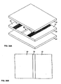
- FIGS. 37A and 37B show the example in which the present invention is applied to a dielectric transmission line.
- FIG. 37A is a partially exploded perspective view of a major part thereof
- FIG. 37B is a cross sectional view thereof.
- dielectric strips 35 and 36 and a dielectric plate 33 having an electrode 34 formed on the upper face thereof are provided between conductor plates 31 and 32, so as to form a non-radiative dielectric transmission line for propagating an electromagnetic wave with the electromagnetic field energy being confined in the dielectric strips 35 and 36.
- the dielectric plate 33 is provided with the spurious mode wave propagation-blocking circuits 3 on both sides of the dielectric strips 35 and 36 by patterning the electrode 34 on the upper face of the dielectric plate 33.
- parallel plate mode electromagnetic waves in the space A1 propagating between the electrode 34 and the upper conductor plate 32 and in the space A2 between the electrode 34 and the lower conductor plate 31 are converted to semi-TEM mode waves by means of the microstrip transmission lines of the spurious mode wave propagation-blocking circuits 3 and are totally reflected. Accordingly, no interference occurs between the dielectric transmission lines and the dielectric transmission lines of the adjacent dielectric strips, which may be caused by leakage waves.
- circular electrode non-formation portions 30 opposed to each other through a dielectric plate 29 are provided in electrodes on the upper and lower faces of the dielectric plate 29.
- a dielectric resonator having the electrode non-formation portions 30 as magnetic walls is formed.
- the resonator functions as a TE010 mode resonator.
- a spurious mode wave propagation-blocking circuit 3 is formed by patterning the electrode on the upper face of the dielectric plate 29. It should be noted that the pattern is simplified to be shown in FIG. 38.
- the spurious mode wave propagation-blocking circuit 3 is the same as that shown in FIG. 31 or FIG. 33B.
- a part of the electromagnetic field energy confined in the dielectric resonator part is radially extended as a parallel plate mode wave from the dielectric resonator as a center between the electrodes provided above and under the dielectric plate 29.
- the parallel plate mode is converted to the mode of the microstrip transmission line by means of the spurious mode wave propagation-blocking circuit 3, and the wave is totally reflected. Accordingly, substantially no parallel plate mode waves are leaked to the outside of the spurious mode wave propagation-blocking circuit 3. Contrarily, substantially no spurious mode waves are leaked from the outside of the spurious mode wave propagation-blocking circuit 3 into the inside thereof (in the direction toward the resonator). Accordingly, no interference occurs between the spurious mode wave propagation-blocking circuit 3 and transmission lines or other resonators on the outside of the spurious mode wave propagation-blocking circuit 3, if they are provided, which may be caused by coupling of leakage waves.
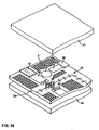
- FIG. 39 is a exploded perspective view showing the configuration of the voltage controlled oscillator.
- the dielectric plate 20 is provided between upper and lower conductor plates 41 and 44 (the upper conductor plate 41 is shown at a distance from the dielectric plate 20 for convenience of the drawing).
- Different types of conductor patterns are formed on the upper and lower faces of the dielectric plate 20.
- a slot transmission line input type FET (millimeter wave GaAsFET) 50 is mounted onto the upper face of the dielectric plate 20.
- Slots 62 and 63 formed of two electrodes, respectively, are arranged at a predetermined interval on the upper face of the dielectric plate 20.
- the slots on the upper face, together with the slots on the lower face, form a plane dielectric transmission line.
- a coplanar transmission line 45 supplies a gate bias voltage and a drain bias voltage to the FET 50.
- Reference numeral 61 designates a thin film resistor.
- the terminal portion of the slot 62 formed on the upper face of the dielectric plate 20 is formed to become thinner toward the top thereof, and the thin film resistor 61 is provided on the upper side of the terminal portion of the slot 62.
- Another slot 65 is formed on the upper face of the dielectric plate 20.
- a slot is also formed on the back side so that the slots sandwich the dielectric plate 20, and thereby, a plane dielectric transmission line is formed.
- a variable capacitance element 60 is mounted so as to extend over the slot 65. The capacitance is varied, depending on an applied voltage. Furthermore, in FIG.
- a conductor non-formation portion 64 for forming a dielectric resonator is provided on the upper face of the dielectric plate 20, and together with a conductor non-formation portion for a dielectric resonator, formed on the back side opposed to the above portion 64 through the dielectric plate 20, constitutes a TE010 mode dielectric resonator in the relevant portion thereof.
- the spurious mode wave propagation-blocking circuits 3 are formed in the cross-hatched portions of the dielectric plate 20 in FIG. 39. Also on the lower face side of the dielectric plate 20, spurious mode wave propagation-blocking circuits are formed in the area thereof opposed to the spurious mode wave propagation-blocking circuits on the upper face. Since the spurious mode wave propagation-blocking circuits 3 are formed as described above, interference between the plane dielectric transmission line comprising the slot 63, the plane dielectric transmission line comprising the slot 65, and the dielectric resonator comprising the conductor non-formation portion 64, which may be caused by leakage waves, is prevented.
- FIGS. 40A and 40B show an example of a high frequency module using a spurious mode wave propagation-blocking circuit comprising the conductor patterns shown in FIG. 33B and arranged two-dimensionally.
- FIG. 40A is a perspective view showing the whole of the high frequency module.
- the high frequency module plural chip integrated circuit parts are mounted onto a substrate 70.
- the high frequency module may be operated, e.g., in a 2 to 30 GHz frequency band.
- FIG 40B is an enlarged plan view showing one of the integrated circuit parts.
- a spiral inductor and a slot transmission line are formed on the substrate. Equivalently, the parts form a matching circuit in which the inductor is connected in parallel to the transmission line.
- the above spurious mode wave propagation-blocking circuit is formed in the area of the module excluding the area where the slot transmission line and the spiral slot inductor are formed.
- a spurious mode wave is generated in that portion.
- the above spurious mode wave propagation-blocking circuit is not provided, and the part simply comprises plane conductors, the above spurious mode wave propagates between the parallel plane conductors, so that it couples to the spiral inductor and causes the parasitic capacity to increase.
- phenomena such as interference or the like, e.g., in a communication module, occurs, or the problem may arise that the characteristics of the respective parts significantly depart from their designed values, which makes it difficult to carry out the design of the whole of the communication module.
- spurious mode wave propagation-blocking circuit is formed in the area excluding where the slot transmission line and the spiral slot inductor are formed as shown in FIG. 40, spurious mode waves, generated in the branched portion and the bend portion of the slot transmission line, can be absorbed in the spurious mode wave propagation-blocking circuit. Accordingly, the spurious mode waves do not couple to the spiral inductor, and the parasitic capacitance is not increased. Thus, the above problems can be solved.
- FIG. 41 is a block diagram showing an example of the configuration of a communication device using the above voltage controlled oscillator.
- a transmission signal is input to an antenna sharing device DPX from a power amplifier PA.
- a reception signal is supplied to a mixer via a low noise amplifier LNA and an RX filter (reception filter).
- a local oscillator PLL which may comprise a phase-locked loop comprises an oscillator OSC and a frequency divider DV for dividing an oscillation signal.
- the local signal is given to the above mixer.
- the above-described voltage controlled oscillator is used as the oscillator OSC.
- the circuit is formed of a strip conductor. Accordingly, the parallel, plane conductors between which a spurious mode wave is to be propagated is simply patterned, which eliminates such problems as arise in formation of conventional through-holes. Moreover, it is not needed especially to provide an inductor and a capacitor as a lumped circuit. Since the circuit can be formed of a strip conductor, the fundamental patterns can be reduced in size and packed to be arranged at a high density in a limited area. Thus, the spurious mode wave propagation-blocking characteristic can be enhanced.
- the frequency band in which a band-stop characteristic is presented can be increased in width, so that propagation of a spurious mode wave can be blocked over a wide band.
- the communication device in a propagation section for propagating a communication signal and in a signal processing section for passing or blocking a predetermined frequency band of communication signals such as a filter or the like, interference can be securely prevented between transmission lines or between transmission lines and a resonator, even if the arrangement intervals of the transmission lines and the resonator are reduced.
- the communication device can be reduced in size as a whole.
Landscapes
- Control Of Motors That Do Not Use Commutators (AREA)
- Waveguides (AREA)
- Inductance-Capacitance Distribution Constants And Capacitance-Resistance Oscillators (AREA)
Claims (4)
- Eine Hochfrequenzschaltungsvorrichtung, die folgende Merkmale aufweist:zumindest zwei Parallelebenenleiter (21, 22; 23, 24, 27, 28; 31, 32, 34; 41, 44),eine Schaltung zum Anregen einer elektromagnetischen Welle, die zwischen den zwei Ebenenleitern vorgesehen ist, undeine Störmoduswellenausbreitungsblockierungsschaltung (3) zum Koppeln mit einer Störmoduswelle, die sich zwischen den zwei Ebenenleitern ausbreitet, um die Ausbreitung der Störmoduswelle zu blockieren, wobei die Schaltung (3) auf einer oder beiden Seiten der zumindest zwei Ebenenleiter gebildet ist, wobei die Störmoduswellenausbreitungsblockierungsschaltung (3) eine Mehrzahl von angeordneten Grundmustern aufweist, die jeweils aus einem Streifenleiter hergestellt sind und eine Mehrtorschaltung bilden, die zumindest drei Tore (Nr. 1, 2, 3, 4) aufweist,dadurch gekennzeichnet, dass
die Mehrtorschaltung eine jeweilige Schaltung mit einer Bandsperrfiltercharakteristik aufweist, die zwischen jedes Paar (Nr. 1, Nr. 2; Nr. 2, Nr. 3; Nr. 3, Nr. 4; Nr. 4, Nr. 1) benachbarter Tore (Nr. 1, Nr. 2, Nr. 3, Nr. 4) geschaltet ist, und
jede jeweilige Schaltung einen Streifenleiter, der die benachbarten Tore (Nr. 1, Nr. 2; Nr. 2, Nr. 3; Nr. 3, Nr. 4; Nr. 4, Nr. 1) jedes Paares verbindet, und eine Streifenübertragungsleitung mit einem offenen Ende aufweist, die eine elektrische Länge aufweist, die bei einer Dienstfrequenz gleich einer 1/4 Wellenlänge ist und die parallel zu dem Streifenleiter zwischen den benachbarten Toren (Nr. 1, Nr. 2; Nr. 2, Nr. 3; Nr. 3, Nr. 4; Nr. 4, Nr. 1) jedes Paares geschaltet ist. - Eine Hochfrequenzschaltungsvorrichtung gemäß Anspruch 1, bei der die Streifenübertragungsleitung jeder Schaltung mit dem Streifenleiter verbunden ist, um die Symmetrie der Schaltung zu durchbrechen.
- Eine Hochfrequenzschaltungsvorrichtung gemäß einem der Ansprüche 1 oder 2, bei der eine Übertragungsleitung, die eine vorbestimmte Impedanz und eine vorbestimmte elektrische Länge aufweist, mit jedem der Eingangs-/Ausgangstore des Grundmusters verbunden ist.
- Eine Kommunikationsvorrichtung, die die Hochfrequenzschaltungsvorrichtung gemäß einem der Ansprüche 1 bis 3 in einem Signalausbreitungsabschnitt oder einem Signalverarbeitungsabschnitt verwendet.
Applications Claiming Priority (5)
| Application Number | Priority Date | Filing Date | Title |
|---|---|---|---|
| JP2000037717 | 2000-02-16 | ||
| JP2000037717 | 2000-02-16 | ||
| JP2001001356 | 2001-01-09 | ||
| JP2001001356A JP3482958B2 (ja) | 2000-02-16 | 2001-01-09 | 高周波回路装置および通信装置 |
| EP01103865A EP1126540B1 (de) | 2000-02-16 | 2001-02-16 | Schaltungsanordnung zur Unterdrückung von parasitären Wellentypen auf planaren Wellenleitern |
Related Parent Applications (1)
| Application Number | Title | Priority Date | Filing Date |
|---|---|---|---|
| EP01103865A Division EP1126540B1 (de) | 2000-02-16 | 2001-02-16 | Schaltungsanordnung zur Unterdrückung von parasitären Wellentypen auf planaren Wellenleitern |
Publications (2)
| Publication Number | Publication Date |
|---|---|
| EP1450433A1 EP1450433A1 (de) | 2004-08-25 |
| EP1450433B1 true EP1450433B1 (de) | 2007-10-10 |
Family
ID=26585442
Family Applications (2)
| Application Number | Title | Priority Date | Filing Date |
|---|---|---|---|
| EP01103865A Expired - Lifetime EP1126540B1 (de) | 2000-02-16 | 2001-02-16 | Schaltungsanordnung zur Unterdrückung von parasitären Wellentypen auf planaren Wellenleitern |
| EP04012771A Expired - Lifetime EP1450433B1 (de) | 2000-02-16 | 2001-02-16 | Schaltungsanordnung zur Unterdrückung von parasitären Wellentypen auf planaren Wellenleitern |
Family Applications Before (1)
| Application Number | Title | Priority Date | Filing Date |
|---|---|---|---|
| EP01103865A Expired - Lifetime EP1126540B1 (de) | 2000-02-16 | 2001-02-16 | Schaltungsanordnung zur Unterdrückung von parasitären Wellentypen auf planaren Wellenleitern |
Country Status (4)
| Country | Link |
|---|---|
| US (1) | US6504456B2 (de) |
| EP (2) | EP1126540B1 (de) |
| JP (1) | JP3482958B2 (de) |
| DE (2) | DE60107883T2 (de) |
Families Citing this family (16)
| Publication number | Priority date | Publication date | Assignee | Title |
|---|---|---|---|---|
| JP3786031B2 (ja) | 2002-02-26 | 2006-06-14 | 株式会社村田製作所 | 高周波回路装置および送受信装置 |
| JP2006526883A (ja) * | 2003-03-06 | 2006-11-24 | サンミナエスシーアイ コーポレイション | バイア構造の高周波性能を最適化する方法 |
| JP4056500B2 (ja) * | 2004-06-28 | 2008-03-05 | 三菱電機株式会社 | 伝送線路基板および半導体パッケージ |
| US7408430B2 (en) | 2004-06-30 | 2008-08-05 | Murata Manufacturing Co., Ltd. | High-frequency circuit device and transmitting and receiving apparatus |
| DE602005022118D1 (de) | 2005-03-24 | 2010-08-12 | Ericsson Telefon Ab L M | Verfahren und anordnung in einem kommunikationssystem zum abliefern von nachrichten an einen empfänger |
| JP4525750B2 (ja) | 2005-04-11 | 2010-08-18 | 株式会社村田製作所 | 平面回路、高周波回路装置および送受信装置 |
| US7626216B2 (en) * | 2005-10-21 | 2009-12-01 | Mckinzie Iii William E | Systems and methods for electromagnetic noise suppression using hybrid electromagnetic bandgap structures |
| US7532083B2 (en) * | 2006-03-23 | 2009-05-12 | Intel Corporation | Active nonlinear transmission line |
| US7649431B2 (en) * | 2006-10-27 | 2010-01-19 | Samsung Electro-Mechanics Co., Ltd. | Band pass filter |
| US7639101B2 (en) * | 2006-11-17 | 2009-12-29 | Superconductor Technologies, Inc. | Low-loss tunable radio frequency filter |
| JP5089502B2 (ja) * | 2008-06-26 | 2012-12-05 | 三菱電機株式会社 | ブランチラインカプラおよびウィルキンソン分配回路 |
| CN101728610B (zh) * | 2008-10-31 | 2013-01-09 | 鸿富锦精密工业(深圳)有限公司 | 带通滤波器 |
| US9584089B2 (en) * | 2013-11-18 | 2017-02-28 | Viasat, Inc. | Nested multi-stage polyphase filter |
| CN111653853B (zh) * | 2020-06-11 | 2021-08-17 | 浙江大学 | 一种无过孔的锯齿型带状线共模滤波电路 |
| CN113471648B (zh) * | 2021-09-03 | 2021-12-14 | 国网江苏省电力有限公司信息通信分公司 | 四模枝节加载谐振器及基于该谐振器的双通带带通滤波器 |
| US11844585B1 (en) | 2023-02-10 | 2023-12-19 | Distalmotion Sa | Surgical robotics systems and devices having a sterile restart, and methods thereof |
Family Cites Families (7)
| Publication number | Priority date | Publication date | Assignee | Title |
|---|---|---|---|---|
| US5023866A (en) * | 1987-02-27 | 1991-06-11 | Motorola, Inc. | Duplexer filter having harmonic rejection to control flyback |
| US6023209A (en) * | 1996-07-05 | 2000-02-08 | Endgate Corporation | Coplanar microwave circuit having suppression of undesired modes |
| US5982339A (en) | 1996-11-26 | 1999-11-09 | Ball Aerospace & Technologies Corp. | Antenna system utilizing a frequency selective surface |
| JPH10200311A (ja) | 1997-01-14 | 1998-07-31 | Nec Corp | 裏面接地導体付きコプレーナウエーブガイド線路 |
| WO1999056338A1 (en) | 1998-04-24 | 1999-11-04 | Endwave Corporation | Coplanar microwave circuit having suppression of undesired modes |
| JP3289694B2 (ja) | 1998-07-24 | 2002-06-10 | 株式会社村田製作所 | 高周波回路装置および通信装置 |
| JP3334680B2 (ja) | 1999-06-03 | 2002-10-15 | 株式会社村田製作所 | 高周波回路装置および通信装置 |
-
2001
- 2001-01-09 JP JP2001001356A patent/JP3482958B2/ja not_active Expired - Fee Related
- 2001-02-15 US US09/784,802 patent/US6504456B2/en not_active Expired - Fee Related
- 2001-02-16 EP EP01103865A patent/EP1126540B1/de not_active Expired - Lifetime
- 2001-02-16 EP EP04012771A patent/EP1450433B1/de not_active Expired - Lifetime
- 2001-02-16 DE DE60107883T patent/DE60107883T2/de not_active Expired - Lifetime
- 2001-02-16 DE DE60130932T patent/DE60130932D1/de not_active Expired - Lifetime
Also Published As
| Publication number | Publication date |
|---|---|
| EP1126540B1 (de) | 2004-12-22 |
| US6504456B2 (en) | 2003-01-07 |
| JP3482958B2 (ja) | 2004-01-06 |
| DE60130932D1 (de) | 2007-11-22 |
| US20010024150A1 (en) | 2001-09-27 |
| EP1126540A3 (de) | 2002-03-27 |
| DE60107883T2 (de) | 2005-12-15 |
| EP1126540A2 (de) | 2001-08-22 |
| JP2001308608A (ja) | 2001-11-02 |
| EP1450433A1 (de) | 2004-08-25 |
| DE60107883D1 (de) | 2005-01-27 |
Similar Documents
| Publication | Publication Date | Title |
|---|---|---|
| JP3289694B2 (ja) | 高周波回路装置および通信装置 | |
| KR100319814B1 (ko) | 유전체 공진기 장치 | |
| US6504456B2 (en) | Communication device having a spurious wave blocking circuit formed of a plural fundamental pattern | |
| KR20100135163A (ko) | 고주파 필터 장치 | |
| KR100287258B1 (ko) | 유전체공진기,유전체필터,듀플렉서및통신장치 | |
| CN115911838A (zh) | 宽带共模吸收的差分馈电式双模贴片天线及天线阵列 | |
| US7492243B2 (en) | Planar circuit, high-frequency circuit device, and transmission and reception apparatus | |
| US6597260B2 (en) | Filter, multiplexer, and communication apparatus | |
| EP1148572A1 (de) | Verbindungsstruktur für Übertragungsleitung, Hochfrequenzmodul und Übertragungsvorrichtung | |
| JP3820234B2 (ja) | 高周波モジュール | |
| US6661315B2 (en) | Resonator, filter, oscillator, duplexer, and communication apparatus | |
| US7408430B2 (en) | High-frequency circuit device and transmitting and receiving apparatus | |
| US10651524B2 (en) | Planar orthomode transducer | |
| EP1058335B1 (de) | Hochfrequenzschaltungsanordnung und Kommunikationsgerät unter Verwendung dieser Anordnung | |
| KR100349082B1 (ko) | 유전체 필터, 송수신 공용기, 및 통신 장치 | |
| US7183874B2 (en) | Casing contained filter | |
| CN117638444B (zh) | 波导滤波功分器 | |
| JP2002335106A (ja) | 高周波回路装置および通信装置 | |
| CN121529136A (zh) | 基于威尔金森功分器和矩形基片集成波导谐振器的无反射带通滤波器 | |
| JPH11308022A (ja) | 線路変換分岐回路およびアンテナ共用装置 | |
| Kim | Development of design Approaches for passive RF and microwave circuits using periodical structures. |
Legal Events
| Date | Code | Title | Description |
|---|---|---|---|
| PUAI | Public reference made under article 153(3) epc to a published international application that has entered the european phase |
Free format text: ORIGINAL CODE: 0009012 |
|
| 17P | Request for examination filed |
Effective date: 20040528 |
|
| AC | Divisional application: reference to earlier application |
Ref document number: 1126540 Country of ref document: EP Kind code of ref document: P |
|
| AK | Designated contracting states |
Kind code of ref document: A1 Designated state(s): DE FR GB |
|
| 17Q | First examination report despatched |
Effective date: 20050121 |
|
| AKX | Designation fees paid |
Designated state(s): DE FR GB |
|
| GRAP | Despatch of communication of intention to grant a patent |
Free format text: ORIGINAL CODE: EPIDOSNIGR1 |
|
| GRAS | Grant fee paid |
Free format text: ORIGINAL CODE: EPIDOSNIGR3 |
|
| GRAA | (expected) grant |
Free format text: ORIGINAL CODE: 0009210 |
|
| RAP1 | Party data changed (applicant data changed or rights of an application transferred) |
Owner name: MURATA MANUFACTURING CO., LTD. |
|
| AC | Divisional application: reference to earlier application |
Ref document number: 1126540 Country of ref document: EP Kind code of ref document: P |
|
| AK | Designated contracting states |
Kind code of ref document: B1 Designated state(s): DE FR GB |
|
| REG | Reference to a national code |
Ref country code: GB Ref legal event code: FG4D |
|
| REF | Corresponds to: |
Ref document number: 60130932 Country of ref document: DE Date of ref document: 20071122 Kind code of ref document: P |
|
| EN | Fr: translation not filed | ||
| PLBE | No opposition filed within time limit |
Free format text: ORIGINAL CODE: 0009261 |
|
| STAA | Information on the status of an ep patent application or granted ep patent |
Free format text: STATUS: NO OPPOSITION FILED WITHIN TIME LIMIT |
|
| 26N | No opposition filed |
Effective date: 20080711 |
|
| PG25 | Lapsed in a contracting state [announced via postgrant information from national office to epo] |
Ref country code: DE Free format text: LAPSE BECAUSE OF FAILURE TO SUBMIT A TRANSLATION OF THE DESCRIPTION OR TO PAY THE FEE WITHIN THE PRESCRIBED TIME-LIMIT Effective date: 20080111 Ref country code: FR Free format text: LAPSE BECAUSE OF FAILURE TO SUBMIT A TRANSLATION OF THE DESCRIPTION OR TO PAY THE FEE WITHIN THE PRESCRIBED TIME-LIMIT Effective date: 20080725 |
|
| PGFP | Annual fee paid to national office [announced via postgrant information from national office to epo] |
Ref country code: GB Payment date: 20120215 Year of fee payment: 12 |
|
| GBPC | Gb: european patent ceased through non-payment of renewal fee |
Effective date: 20130216 |
|
| PG25 | Lapsed in a contracting state [announced via postgrant information from national office to epo] |
Ref country code: GB Free format text: LAPSE BECAUSE OF NON-PAYMENT OF DUE FEES Effective date: 20130216 |