EP1450554B1 - Capteur d'images CMOS avec un nombre réduit de circuits de lecture de colonnes - Google Patents
Capteur d'images CMOS avec un nombre réduit de circuits de lecture de colonnes Download PDFInfo
- Publication number
- EP1450554B1 EP1450554B1 EP04250131.2A EP04250131A EP1450554B1 EP 1450554 B1 EP1450554 B1 EP 1450554B1 EP 04250131 A EP04250131 A EP 04250131A EP 1450554 B1 EP1450554 B1 EP 1450554B1
- Authority
- EP
- European Patent Office
- Prior art keywords
- column readout
- group
- readout circuits
- pixels
- blocks
- Prior art date
- Legal status (The legal status is an assumption and is not a legal conclusion. Google has not performed a legal analysis and makes no representation as to the accuracy of the status listed.)
- Expired - Lifetime
Links
- 239000003990 capacitor Substances 0.000 claims description 25
- 238000000034 method Methods 0.000 claims description 12
- 230000002596 correlated effect Effects 0.000 claims description 7
- 238000005070 sampling Methods 0.000 claims description 7
- XUIMIQQOPSSXEZ-UHFFFAOYSA-N Silicon Chemical compound [Si] XUIMIQQOPSSXEZ-UHFFFAOYSA-N 0.000 description 2
- 230000010354 integration Effects 0.000 description 2
- 239000000463 material Substances 0.000 description 2
- 229910052710 silicon Inorganic materials 0.000 description 2
- 239000010703 silicon Substances 0.000 description 2
- 230000004075 alteration Effects 0.000 description 1
- 230000003321 amplification Effects 0.000 description 1
- 238000006243 chemical reaction Methods 0.000 description 1
- 230000000875 corresponding effect Effects 0.000 description 1
- 238000010586 diagram Methods 0.000 description 1
- 239000002184 metal Substances 0.000 description 1
- 238000003199 nucleic acid amplification method Methods 0.000 description 1
- 230000003287 optical effect Effects 0.000 description 1
- 239000004065 semiconductor Substances 0.000 description 1
- 238000006467 substitution reaction Methods 0.000 description 1
Images
Classifications
-
- H—ELECTRICITY
- H04—ELECTRIC COMMUNICATION TECHNIQUE
- H04N—PICTORIAL COMMUNICATION, e.g. TELEVISION
- H04N25/00—Circuitry of solid-state image sensors [SSIS]; Control thereof
- H04N25/70—SSIS architectures; Circuits associated therewith
- H04N25/76—Addressed sensors, e.g. MOS or CMOS sensors
- H04N25/767—Horizontal readout lines, multiplexers or registers
-
- H—ELECTRICITY
- H04—ELECTRIC COMMUNICATION TECHNIQUE
- H04N—PICTORIAL COMMUNICATION, e.g. TELEVISION
- H04N25/00—Circuitry of solid-state image sensors [SSIS]; Control thereof
- H04N25/70—SSIS architectures; Circuits associated therewith
- H04N25/76—Addressed sensors, e.g. MOS or CMOS sensors
- H04N25/78—Readout circuits for addressed sensors, e.g. output amplifiers or A/D converters
Definitions
- the present invention relates to CMOS image sensors, and more particularly, to an image sensor that uses multiplexed column readout circuits.
- Image sensors are used to produce an image representing an object.
- the image sensors include rows and columns of pixels.
- the pixels generate small photo signals proportional to light reflected from an object to be imaged.
- the photo signal is read and processed by signal processing circuitry to create an image representing the object.
- Pixels belonging to the same column are usually connected at a common output node from where the signal is read out. Each pixel in a same bitline is individually controlled to read out at the common output node.
- a column readout circuit is provided to read out and amplify the photo signal.
- a column readout circuit is also referred to as a line buffer.
- a pixel typically includes a driving device that receives an electronic signal indicative of an intensity of light detected by the image sensor and drives a current proportional to the intensity (the photo signal), to a bitline to which the pixel cell is coupled. Following signal integration, pixels of a selected row are accessed by asserting a row select signal to each pixel of the selected row.
- the column readout circuit in some image sensors, is used to remove thermal noise, fixed pattern noise, and other types of noise. This is done by having the column readout circuit sample the output of the pixel during a reset period. The column readout circuit then subtracts the reset signal from the photo signal. This type of readout circuit is sometimes referred to as a correlated double sampling circuit.
- a second stage column readout circuit is used to further amplify the photo signal and to eliminate noise caused by the first stage column readout circuit.
- An example of a correlated double sampling column readout circuit is seen in U.S. Patent No. 6,222,175 . Another example is shown in our co-pending U.S. Patent Application Serial No 10/109,142 filed March 27, 2002 entitled COLUMN READOUT CIRCUIT WITH INCREASED SIGNAL RANGE FOR CMOS IMAGE SENSOR.
- one column readout circuit is associated with each column of the pixel array. For a pixel array with thousands of columns, this requires thousands of column readout circuits. As the drive for smaller and smaller integrated circuits continues, the large number of column readout circuits (which are relatively large), may require an inordinate amount of silicon real estate.
- the column readout circuits may make up the bulk of the entire circuit. Further, the large number of column readout circuits may require a large amount of current.
- a linear sensor is generally characterized as having a pixel array that has much more columns than rows. For example, a linear sensor may have less than five rows, yet thousands of columns.
- One application for a linear sensor is for an optical scanner or reader.
- US2003/0011829 describes methods and devices for reading out an image sensor with reduced delay times between the reading out of different lines.
- the method of first embodiment reads out each line of an image sensor in at least two overlapping sequences, whereby each sequence comprises a succession of blanking times and pixel readout periods.
- the timing of the sequences is such that the readout periods of different sequences are interleaved.
- JP-2000/078474 discloses an image pickup device which attains low power consumption and noise by providing a shared vertical output line to each photoelectric conversion part in a unit cell.
- the present invention provides an image sensor according to Claim 1.
- the present invention provides a method for reading out pixel signals from a row of pixels, according to Claim 5.
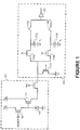
- an active pixel 101 is shown connected to a column readout circuit 103.
- the connection is typically made through a signal line that is the same for all pixels within a column, and is commonly referred to as a column signal line.
- the active pixel 101 includes a photodiode 105, a reset transistor 107, pixel output transistor 109, and row select transistor 111.
- the configuration of the active pixel 101 is conventional in the prior art.
- the photodiode 105 provides a light signal output that is indicative of the amount of light impinging on the photodiode 105.
- the light signal is used to modulate the pixel output transistor 109 in order to output a photo signal if the row select (RS) transistor 111 is turned on.
- the pixel output transistor 109 is also referred to as being in source follower configuration.
- the reset transistor 107 is used to reset the pixel 101 for the next signal integration period.
- the pixel 101 in one embodiment uses a photodiode 105, the pixel 101 may use a photogate or a pinned photodiode.
- the column readout circuit 103 described herein is merely one example of a simplified column readout circuit and should not be construed as limiting. The present invention may be used with other types of column readout circuits.
- the column readout circuit 103 includes two branches: a first branch for capturing a reset signal and a second branch for capturing the photo signal. Specifically, the source of the pixel output transistor is connected, through row select transistor 111, to both the first and second branches.
- the use of the two branches allows for correlated double sampling, a technique useful for minimizing 1/f noise and fixed pattern noise. Note that for correlated double sampling, typically a shorting transistor is used between the two branches. However, for clarity purposes, the shorting transistor is omitted from the readout circuit shown in Figure 1 .
- the first and second branches are essentially structured the same.
- like elements are designated with like numerals, except that the first branch for capturing the reset signal is designated with an "a" and the second branch for capturing the photo signal is designated with a "b".
- the readout circuit operates on two input signals: the photo signal and the reset signal.
- the photo signal and the reset signal are referred to collectively as "pixel signals".
- the column readout circuit 103 also includes a load transistor 113 of the pixel output transistor 109.
- the first and second each include branch select transistors 115a and 115b. These act as switches to select the branch to which the signal output by the active pixel 101 is directed.
- capacitors 117a and 117b Downstream of the branch select transistors 115a-115b are capacitors 117a and 117b.
- the term downstream refers to locations in the signal path subsequent to a reference location.
- the capacitors 117a-117b have a first plate connected to a voltage V L , which may be V SS or ground.
- the second plate of the capacitor is connected to the drain of the select transistors 115a-115b.
- the capacitors 117a-117b may be poly-poly capacitors, metal-metal capacitors, MOS capacitors, or any type of conventional capacitor formed in a semiconductor process. The capacitors are used to store the photo signal and the reset signal in order to perform the correlated sampling.
- the second plate of the capacitors are connected to read switches 119a-119b. These read switches 119a-119b selectively open and close to read out the various signals on the capacitors 117a-117b through a buffer 121. These signals are then subsequently processed to extract the signal from the pixel 101.
- a reset signal (also referred to as a reference signal or a black signal) must be stored in capacitor 115a and a photo signal must be stored in capacitor 115b.
- the various switches, such as RS, 115a-b, 119a-b, and Reset operate in a predetermined sequence to facilitate readout of the pixel signal.
- a CMOS image sensor includes an array of pixels formed into columns and rows.
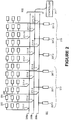
- an image sensor 201 includes a pixel array 203 formed by a two-dimensional array of pixels 205.
- the pixels 205 may be active pixels as described above, which include amplification within each pixel 205.
- the configuration of the active pixels 205 is conventional. In operation, the pixels 205 provides a light signal output that is indicative of the amount of light impinging on the pixel. At the bottom portion of the pixel array 203 are a plurality of column readout circuits 207. Note that the column readout circuits 207 are shown in the "bottom" of Figure 1 for convenience purposes, and in actuality, the column readout circuits 207 may be placed almost anywhere on the integrated circuit relative to the pixel array 203.
- two groups of column readout circuits 207 work together in alternating fashion.
- a first group 213 and a second group 215 are shown.
- the first group 213 and the second group 215 work alternately, such that when the first group 213 is storing the signals onto the storage capacitors (117a-b) of its column readout circuits 207-1, the second group 215 is reading out the signals (via switches 119a and 119b) from its column readout circuits 207-2.
- the second group 215 is storing the signals onto the storage capacitors (117a-b)
- the first group 213 is reading out the signals (via switches 119a and 119b).
- this "multiplexing" will require multiplexer signal busses 209 and block selection switches 211. These can be easily generated using shift register or other methods known in the art.
- each group 213 and 215 it may take several repetitions of switching before an entire row of pixels can be read out.
- the signals from the first three pixels of a row are stored by column readout circuits 207-1 of the first group 213.
- This will require the block selection switches 211-1, 211-2, and 211-3 for the first three pixels be turned “on” so that the column readout circuits 207-1 of the first group 213 can receive the signals.
- All of the other block selection switches 211-4 through 211-12 for the other nine pixels are turned "off' to avoid signal interference.
- the column readout circuits 207-1 of the first group 213 will then read out the signals to further processing circuitry (not shown).
- the block selection switches 211-1 through 211-3 for the first three pixels will switch off.
- the block selection switches 211-4 through 211-6 will switch on and route their signals to the column readout circuits 207-2 of the second group.
- the remaining block selection switches 211-7 through 211-12 will remain off.
- the column readout circuits 207-2 of the second group 215 will then read out the signals (referred to as processed signals) to further processing circuitry (not shown).
- the block selection switches 211-4 through 211-6 for the pixels 4-6 will switch off.
- the block selection switches 211-7 through 211-9 will switch on and route their signals to the column readout circuits 207-1 of the first group 213, which have now finished transferring the signals from the first three pixels out.
- the remaining block selection switches 211-1 through 211-6 and 211-10 through 211-12 will remain off. This alternating process will continue until all of the pixels for a particularly row have been read out. Further, the remaining rows of the pixel array can be read out in a similar manner.
- the control of the block selection switches 211-1 through 211-12 can be performed by a controller 217 that can be programmed to activate and deactivate the block selection switches to implement the alternating readout through the column readout circuits 207.
- Figure 2 is for a row having twelve pixels (i.e., columns) and for each group of column readout circuits to have three column readout circuits, it can be appreciated that the concepts and operation of the present invention can be extrapolated to a wide variety of combinations.
- the number of column readout circuits 207 is substantially less than the number of columns in the pixel array 203.
- the pixel array 203 includes twelve columns and three rows.
- the present invention may be used with any arbitrary sized pixel array 203.
- the number of columns in the pixel array 203 is twelve, but can also be referred to generally as "M" number of columns or simply M columns.
- the M columns are divided for signal readout purposes into N blocks.
- the M columns may be divided into four blocks (N) of three columns each.
- each row is divided into blocks of three pixels each (M divided by N).
- N may be six.
- each block consists of two columns.
- each row is divided into blocks of two pixels each (M divided by N).
- the number of column readout circuits 207 in both the first and second groups 213 and 215 is then equal to the number of pixels in a block. For Figure 2 with a value of four for N, this results in blocks of three pixels. Thus, both the first and second groups 213 and 215 have three column readout circuits 207 each. Thus, in this example, only six column readout circuits 207 are required, instead of the conventional twelve column readout circuits.
- the present invention takes advantage of the fact that the time it takes to store a signal onto the capacitors of the column readout circuit is generally significantly less than the total readout time allotted for reading out a row.
- the row select (RS) signal applied to a particular row is much longer than the time needed to drive the signal onto the capacitors in the column readout circuit. This provides the opportunity to re-use the column readout circuits 207 for other pixels in the same row.
- the number of column readout circuits will increase and the number of signal busses 209 will increase, occupying more space.
Landscapes
- Engineering & Computer Science (AREA)
- Multimedia (AREA)
- Signal Processing (AREA)
- Transforming Light Signals Into Electric Signals (AREA)
- Solid State Image Pick-Up Elements (AREA)
Claims (7)
- Capteur d'image (201) comprenant :une pluralité de pixels (205) agencés en tant que réseau de pixels (203) comportant M colonnes, lesdites M colonnes étant groupées en N blocs, chacun desdits N blocs comportant M/N colonnes ;un premier groupe (213) de circuits de lecture de colonne comportant M/N circuits de lecture de colonne (207-1) pour lire les signaux de pixel provenant desdits pixels (205) ;un deuxième groupe (215) de circuits de lecture de colonne comportant M/N circuits de lecture de colonne (207-2) pour lire les signaux de pixel provenant desdits pixels ; etun système de bus de multiplexeur comportant M commutateurs de sélection (211) pour commuter de manière sélective les signaux de pixel provenant de l'un desdits N blocs en tant qu'entrée dans ledit premier groupe (213) de circuits de lecture de colonne et d'un autre desdits N blocs en tant qu'entrée dans ledit deuxième groupe (215) de circuits de lecture de colonne et pour répéter la commutation sélective des signaux de pixel soit dans le premier groupe, soit dans le deuxième groupe pour chaque bloc restant jusqu'à ce que la totalité des N blocs aient été traités soit par ledit premier groupe, soit par ledit deuxième groupe, dans lequel ledit premier groupe de circuits de lecture de colonne et ledit deuxième groupe de circuits de lecture de colonne fonctionnent alternativement de sorte que, lorsque ledit premier groupe de circuits de lecture de colonne mémorise un signal de réinitialisation et un signal photoélectrique provenant des pixels de l'un desdits N blocs, ledit deuxième groupe de circuits de lecture de colonne transfère les signaux traités provenant des pixels d'un autre desdits N blocs ;dans lequel chaque circuit de lecture à la fois dans les premier et deuxième groupes comprend deux condensateurs (117a, 117b) pour mémoriser ledit signal de réinitialisation et ledit signal photoélectrique provenant dudit pixel (205) respectivement, et deux commutateurs (119a, 119b) pour lire les signaux provenant des condensateurs (117a, 117b) ;dans lequel N est supérieur 2 de sorte que le nombre total de circuits de lecture de colonne est inférieur au nombre de colonnes M.
- Capteur d'image selon la revendication 1, dans lequel lesdits pixels (205) sont des pixels actifs.
- Capteur d'image selon la revendication 1, dans lequel ledit premier groupe (213) et ledit deuxième groupe (215) comprennent le même nombre de circuits de lecture de colonne (207).
- Capteur d'image selon la revendication 1, dans lequel lesdits circuits de lecture de colonne (207) sont des circuits de lecture à double échantillonnage corrélé.
- Procédé pour lire les signaux de pixel provenant d'une rangée de pixels (205), ladite rangée de pixels comprenant M pixels, lesdits M pixels étant groupés en N blocs, chacun desdits N blocs comportant M/N colonnes, le procédé comprenantla fourniture d'un premier groupe (213) de circuits de lecture de colonne (207) comportant M/N circuits de lecture de colonne (207-1) pour lire les signaux de pixel provenant desdits pixels ;la fourniture d'un deuxième groupe (215) de circuits de lecture de colonne (207), comportant M/N circuits de lecture de colonne (207-2) pour lire les signaux de pixel provenant desdits pixels ; etl'utilisation d'un système de bus de multiplexeur comportant M commutateurs de sélection (211) pour commuter de manière sélective les signaux de pixel provenant de l'un desdits N blocs en tant qu'entrée dans ledit premier groupe (213) de circuits de lecture de colonne et d'un autre desdits N blocs en tant qu'entrée dans ledit deuxième groupe (215) de circuits de lecture de colonne et pour répéter la commutation sélective des signaux de pixel soit dans le premier groupe, soit dans le deuxième groupe pour chaque bloc restant jusqu'à ce que la totalité des N blocs aient été traités soit par ledit premier groupe, soit par ledit deuxième groupe, dans lequel ledit premier groupe de circuits de lecture de colonne et ledit deuxième groupe de circuits de lecture de colonne fonctionnent alternativement de sorte que, lorsque ledit premier groupe de circuits de lecture de colonne mémorise un signal de réinitialisation et un signal photoélectrique provenant des pixels de l'un desdits N blocs, ledit deuxième groupe de circuits de lecture de colonne transfère les signaux traités provenant des pixels d'un autre desdits N blocs ;dans lequel chaque circuit de lecture à la fois dans les premier et deuxième groupes comprend deux condensateurs (117a, 117b) pour mémoriser ledit signal de réinitialisation et ledit signal photoélectrique provenant dudit pixel (205) respectivement, et deux commutateurs (119a, 119b) pour lire les signaux provenant des condensateurs (117a, 117b) ;dans lequel N est supérieur à 2 de sorte que le nombre total de circuits de lecture de colonne est inférieur au nombre de colonnes M.
- Procédé selon la revendication 5, dans lequel ledit premier groupe (213) et ledit deuxième groupe (215) comprennent le même nombre de circuits de lecture de colonne (207).
- Procédé selon la revendication 5, dans lequel lesdits circuits de lecture de colonne (207) sont des circuits de lecture à double échantillonnage corrélé.
Applications Claiming Priority (2)
| Application Number | Priority Date | Filing Date | Title |
|---|---|---|---|
| US368949 | 1982-04-16 | ||
| US10/368,949 US6953923B2 (en) | 2003-02-18 | 2003-02-18 | CMOS image sensor having reduced numbers of column readout circuits |
Publications (3)
| Publication Number | Publication Date |
|---|---|
| EP1450554A2 EP1450554A2 (fr) | 2004-08-25 |
| EP1450554A3 EP1450554A3 (fr) | 2006-02-08 |
| EP1450554B1 true EP1450554B1 (fr) | 2018-03-21 |
Family
ID=32736414
Family Applications (1)
| Application Number | Title | Priority Date | Filing Date |
|---|---|---|---|
| EP04250131.2A Expired - Lifetime EP1450554B1 (fr) | 2003-02-18 | 2004-01-13 | Capteur d'images CMOS avec un nombre réduit de circuits de lecture de colonnes |
Country Status (4)
| Country | Link |
|---|---|
| US (1) | US6953923B2 (fr) |
| EP (1) | EP1450554B1 (fr) |
| CN (1) | CN1326385C (fr) |
| TW (1) | TWI235602B (fr) |
Families Citing this family (35)
| Publication number | Priority date | Publication date | Assignee | Title |
|---|---|---|---|---|
| US7471324B2 (en) * | 2002-08-28 | 2008-12-30 | Aptina Imaging Corporation | Amplifier shared between two columns in CMOS sensor |
| US7365784B2 (en) * | 2003-04-15 | 2008-04-29 | Micron Technology, Inc. | Column sample-and-hold cell for CMOS APS sensor |
| US20060187329A1 (en) * | 2005-02-24 | 2006-08-24 | Micron Technology, Inc. | Clamped capacitor readout noise rejection circuit for imagers |
| US7554066B2 (en) * | 2005-04-13 | 2009-06-30 | Aptina Imaging Corporation | Method and apparatus employing dynamic element matching for reduction of column-wise fixed pattern noise in a solid state imaging sensor |
| US7659925B2 (en) * | 2005-10-04 | 2010-02-09 | Alexander Krymski | High speed CMOS image sensor circuits with memory readout |
| CN101455070B (zh) * | 2006-05-22 | 2014-06-11 | 汤姆森特许公司 | 图像传感器和用于读出图像传感器的像素的方法 |
| JP4054839B1 (ja) * | 2007-03-02 | 2008-03-05 | キヤノン株式会社 | 光電変換装置およびそれを用いた撮像システム |
| US7488928B2 (en) * | 2007-04-20 | 2009-02-10 | Alexander Krymski | Image sensor circuits and methods with multiple readout lines per column of pixel circuits |
| DE102007027463B4 (de) * | 2007-06-14 | 2021-03-25 | Arnold & Richter Cine Technik Gmbh & Co. Betriebs Kg | Bildsensor |
| US7746400B2 (en) * | 2007-07-31 | 2010-06-29 | Aptina Imaging Corporation | Method, apparatus, and system providing multi-column shared readout for imagers |
| US7995124B2 (en) * | 2007-09-14 | 2011-08-09 | Omnivision Technologies, Inc. | Image sensor apparatus and method for improved dynamic range with multiple readout circuit paths |
| DE102007058973A1 (de) * | 2007-12-07 | 2009-06-18 | Arnold & Richter Cine Technik Gmbh & Co. Betriebs Kg | Bildsensor |
| JP5151507B2 (ja) * | 2008-01-29 | 2013-02-27 | ソニー株式会社 | 固体撮像素子、固体撮像素子の信号読み出し方法および撮像装置 |
| US9019411B2 (en) | 2008-05-01 | 2015-04-28 | Alexander Krymski | Image sensors and methods with pipelined readout |
| US8174603B2 (en) * | 2008-05-01 | 2012-05-08 | Alexander Krymski | Image sensors and methods with antiblooming channels and two side driving of control signals |
| US7804438B2 (en) * | 2008-05-02 | 2010-09-28 | Alexander Krymski | Image sensors and dual ramp analog-to-digital converters and methods |
| US8081247B2 (en) * | 2008-06-18 | 2011-12-20 | Omnivision Technologies, Inc. | Partial row readout for image sensor |
| TWI387325B (zh) * | 2008-10-09 | 2013-02-21 | Silicon Motion Inc | 影像擷取裝置與影像前處理方法 |
| CN101841633B (zh) * | 2009-03-19 | 2013-09-04 | 英属开曼群岛商恒景科技股份有限公司 | 图像传感器的读出电路 |
| US8411184B2 (en) * | 2009-12-22 | 2013-04-02 | Omnivision Technologies, Inc. | Column output circuits for image sensors |
| US8785831B2 (en) * | 2011-01-05 | 2014-07-22 | Luxima Technology LLC | Image sensors and methods with high speed global shutter pixels |
| US8723093B2 (en) | 2011-01-10 | 2014-05-13 | Alexander Krymski | Image sensors and methods with shared control lines |
| TWI451758B (zh) * | 2011-04-07 | 2014-09-01 | 義隆電子股份有限公司 | Active image sensing circuit and its sensing method |
| US8732433B2 (en) | 2011-08-26 | 2014-05-20 | Micron Technology, Inc. | Apparatuses and methods for providing data from multiple memories |
| DE102011120099B4 (de) | 2011-12-02 | 2024-05-29 | Arnold & Richter Cine Technik Gmbh & Co. Betriebs Kg | Bildsensor und Verfahren zum Auslesen eines Bildsensors |
| JP2014003542A (ja) * | 2012-06-20 | 2014-01-09 | Canon Inc | 検出装置、検出システム及び検出装置の駆動方法 |
| US9369648B2 (en) | 2013-06-18 | 2016-06-14 | Alexander Krymski | Image sensors, methods, and pixels with tri-level biased transfer gates |
| CN109068023B (zh) * | 2018-07-26 | 2020-12-18 | 西安理工大学 | 超大面阵图像传感器的读出电路同步控制系统及控制方法 |
| CN108965674B (zh) * | 2018-08-23 | 2024-04-09 | Oppo广东移动通信有限公司 | 一种感光芯片、摄像头模组及电子设备 |
| CN110062182B (zh) * | 2019-04-16 | 2021-03-30 | 长春长光辰芯光电技术有限公司 | 高帧频面阵图像传感器像素信号交错分时读出方法 |
| CN110309820B (zh) * | 2019-08-28 | 2020-01-07 | 深圳市汇顶科技股份有限公司 | 指纹检测的装置和电子设备 |
| WO2021035583A1 (fr) | 2019-08-28 | 2021-03-04 | 深圳市汇顶科技股份有限公司 | Appareil de détection d'empreinte digitale et dispositif électronique |
| US11363226B2 (en) | 2020-04-27 | 2022-06-14 | Shenzhen GOODIX Technology Co., Ltd. | Ping pong readout structure in image sensor with dual pixel supply |
| US11658202B2 (en) | 2020-05-15 | 2023-05-23 | Omnivision Technologies, Inc. | Dual row select pixel for fast pixel binning |
| CN114355384B (zh) * | 2020-07-07 | 2024-01-02 | 柳州阜民科技有限公司 | 飞行时间tof系统和电子设备 |
Family Cites Families (8)
| Publication number | Priority date | Publication date | Assignee | Title |
|---|---|---|---|---|
| US5461425A (en) * | 1994-02-15 | 1995-10-24 | Stanford University | CMOS image sensor with pixel level A/D conversion |
| US6366320B1 (en) * | 1997-12-08 | 2002-04-02 | Intel Corporation | High speed readout architecture for analog storage arrays |
| US6697108B1 (en) * | 1997-12-31 | 2004-02-24 | Texas Instruments Incorporated | Fast frame readout architecture for array sensors with integrated correlated double sampling system |
| AU3074899A (en) * | 1998-03-09 | 1999-09-27 | Photobit Corporation | Readout circuit with gain and analog-to-digital conversion for image sensor |
| US6222175B1 (en) * | 1998-03-10 | 2001-04-24 | Photobit Corporation | Charge-domain analog readout for an image sensor |
| US6512546B1 (en) * | 1998-07-17 | 2003-01-28 | Analog Devices, Inc. | Image sensor using multiple array readout lines |
| JP3559714B2 (ja) * | 1998-09-02 | 2004-09-02 | キヤノン株式会社 | 撮像装置およびそれを用いた撮像システム |
| US7106915B2 (en) * | 2001-07-16 | 2006-09-12 | Cypress Semiconductor Corporation | Methods and devices for reading out an image sensor with reduced delay time between lines |
-
2003
- 2003-02-18 US US10/368,949 patent/US6953923B2/en not_active Expired - Lifetime
-
2004
- 2004-01-13 EP EP04250131.2A patent/EP1450554B1/fr not_active Expired - Lifetime
- 2004-01-16 TW TW093101288A patent/TWI235602B/zh not_active IP Right Cessation
- 2004-02-18 CN CNB2004100054366A patent/CN1326385C/zh not_active Expired - Lifetime
Non-Patent Citations (1)
| Title |
|---|
| None * |
Also Published As
| Publication number | Publication date |
|---|---|
| EP1450554A2 (fr) | 2004-08-25 |
| TW200417246A (en) | 2004-09-01 |
| TWI235602B (en) | 2005-07-01 |
| EP1450554A3 (fr) | 2006-02-08 |
| US6953923B2 (en) | 2005-10-11 |
| US20040159771A1 (en) | 2004-08-19 |
| CN1326385C (zh) | 2007-07-11 |
| CN1523878A (zh) | 2004-08-25 |
Similar Documents
| Publication | Publication Date | Title |
|---|---|---|
| EP1450554B1 (fr) | Capteur d'images CMOS avec un nombre réduit de circuits de lecture de colonnes | |
| USRE34908E (en) | 3-transistor source follower-per-detector unit cell for 2-dimensional focal plane arrays | |
| EP0809300B1 (fr) | Capteur d'images à éléments d'image actifs avec remise à zéro individuelle des éléments d'image | |
| US8310578B2 (en) | Image sensors and methods with column readout circuits | |
| US5345266A (en) | Matrix array image sensor chip | |
| US8723093B2 (en) | Image sensors and methods with shared control lines | |
| JP3521109B2 (ja) | 動き検出用固体撮像装置 | |
| US6525304B1 (en) | Circuitry for converting analog signals from pixel sensor to a digital and for storing the digital signal | |
| KR100904716B1 (ko) | 수광 효율이 향상된 이미지 센서 | |
| US20080246869A1 (en) | Differential readout from pixels in CMOS sensor | |
| US10194106B2 (en) | Image sensor and sensing method thereof | |
| US20040246354A1 (en) | CMOS image sensor having high speed sub sampling | |
| KR20060050050A (ko) | 고체 촬상 장치 | |
| US7116367B2 (en) | Solid-state image pickup apparatus having a reset transistor controlled by an output line | |
| US7639296B2 (en) | Solid state imaging apparatus | |
| US11343454B2 (en) | Imaging systems and methods for performing pixel binning and variable integration for analog domain regional feature extraction | |
| US7471324B2 (en) | Amplifier shared between two columns in CMOS sensor | |
| EP1919192B1 (fr) | Procédé et appareil pour la suppression du bruit kTC dans un capteur d'image CMOS linéaire | |
| JP4056506B2 (ja) | 画素構造のアレイ、および画素構造の行または列の選択方法 | |
| US6486912B1 (en) | Image sensor with sampling control system | |
| EP1277235B1 (fr) | Bus video pour imageurs multiresolution a grande vitesse et procede correspondant | |
| US20080225149A1 (en) | Column sample-and-hold cell for CMOS APS sensor | |
| JP3956875B2 (ja) | 固体撮像装置 | |
| EP2611142B1 (fr) | Dispositif d'image avec lecteur des colonnes | |
| KR100595801B1 (ko) | 고체 촬상 장치, 그 구동 방법 및 카메라 |
Legal Events
| Date | Code | Title | Description |
|---|---|---|---|
| PUAI | Public reference made under article 153(3) epc to a published international application that has entered the european phase |
Free format text: ORIGINAL CODE: 0009012 |
|
| AK | Designated contracting states |
Kind code of ref document: A2 Designated state(s): AT BE BG CH CY CZ DE DK EE ES FI FR GB GR HU IE IT LI LU MC NL PT RO SE SI SK TR |
|
| AX | Request for extension of the european patent |
Extension state: AL LT LV MK |
|
| RIN1 | Information on inventor provided before grant (corrected) |
Inventor name: YANG, HONGLI Inventor name: HE, XINPINGC/O OMNIVISION TECHNOLOGIES, INC. |
|
| PUAL | Search report despatched |
Free format text: ORIGINAL CODE: 0009013 |
|
| AK | Designated contracting states |
Kind code of ref document: A3 Designated state(s): AT BE BG CH CY CZ DE DK EE ES FI FR GB GR HU IE IT LI LU MC NL PT RO SE SI SK TR |
|
| AX | Request for extension of the european patent |
Extension state: AL LT LV MK |
|
| 17P | Request for examination filed |
Effective date: 20060420 |
|
| 17Q | First examination report despatched |
Effective date: 20060713 |
|
| AKX | Designation fees paid |
Designated state(s): AT BE BG CH CY CZ DE DK EE ES FI FR GB GR HU IE IT LI LU MC NL PT RO SE SI SK TR |
|
| REG | Reference to a national code |
Ref country code: DE Ref legal event code: R079 Ref document number: 602004052487 Country of ref document: DE Free format text: PREVIOUS MAIN CLASS: H04N0003150000 Ipc: H04N0005374000 |
|
| RIC1 | Information provided on ipc code assigned before grant |
Ipc: H04N 5/374 20110101AFI20170824BHEP |
|
| GRAP | Despatch of communication of intention to grant a patent |
Free format text: ORIGINAL CODE: EPIDOSNIGR1 |
|
| STAA | Information on the status of an ep patent application or granted ep patent |
Free format text: STATUS: GRANT OF PATENT IS INTENDED |
|
| INTG | Intention to grant announced |
Effective date: 20171005 |
|
| RIN1 | Information on inventor provided before grant (corrected) |
Inventor name: YANG, HONGLI Inventor name: HE, XINPING |
|
| RAP1 | Party data changed (applicant data changed or rights of an application transferred) |
Owner name: OMNIVISION TECHNOLOGIES, INC. |
|
| GRAS | Grant fee paid |
Free format text: ORIGINAL CODE: EPIDOSNIGR3 |
|
| GRAA | (expected) grant |
Free format text: ORIGINAL CODE: 0009210 |
|
| STAA | Information on the status of an ep patent application or granted ep patent |
Free format text: STATUS: THE PATENT HAS BEEN GRANTED |
|
| AK | Designated contracting states |
Kind code of ref document: B1 Designated state(s): AT BE BG CH CY CZ DE DK EE ES FI FR GB GR HU IE IT LI LU MC NL PT RO SE SI SK TR |
|
| REG | Reference to a national code |
Ref country code: GB Ref legal event code: FG4D |
|
| REG | Reference to a national code |
Ref country code: CH Ref legal event code: EP |
|
| REG | Reference to a national code |
Ref country code: AT Ref legal event code: REF Ref document number: 982330 Country of ref document: AT Kind code of ref document: T Effective date: 20180415 |
|
| REG | Reference to a national code |
Ref country code: IE Ref legal event code: FG4D |
|
| REG | Reference to a national code |
Ref country code: DE Ref legal event code: R096 Ref document number: 602004052487 Country of ref document: DE |
|
| REG | Reference to a national code |
Ref country code: NL Ref legal event code: MP Effective date: 20180321 |
|
| PG25 | Lapsed in a contracting state [announced via postgrant information from national office to epo] |
Ref country code: FI Free format text: LAPSE BECAUSE OF FAILURE TO SUBMIT A TRANSLATION OF THE DESCRIPTION OR TO PAY THE FEE WITHIN THE PRESCRIBED TIME-LIMIT Effective date: 20180321 Ref country code: CY Free format text: LAPSE BECAUSE OF FAILURE TO SUBMIT A TRANSLATION OF THE DESCRIPTION OR TO PAY THE FEE WITHIN THE PRESCRIBED TIME-LIMIT Effective date: 20180321 |
|
| REG | Reference to a national code |
Ref country code: AT Ref legal event code: MK05 Ref document number: 982330 Country of ref document: AT Kind code of ref document: T Effective date: 20180321 |
|
| PG25 | Lapsed in a contracting state [announced via postgrant information from national office to epo] |
Ref country code: GR Free format text: LAPSE BECAUSE OF FAILURE TO SUBMIT A TRANSLATION OF THE DESCRIPTION OR TO PAY THE FEE WITHIN THE PRESCRIBED TIME-LIMIT Effective date: 20180622 Ref country code: BG Free format text: LAPSE BECAUSE OF FAILURE TO SUBMIT A TRANSLATION OF THE DESCRIPTION OR TO PAY THE FEE WITHIN THE PRESCRIBED TIME-LIMIT Effective date: 20180621 Ref country code: SE Free format text: LAPSE BECAUSE OF FAILURE TO SUBMIT A TRANSLATION OF THE DESCRIPTION OR TO PAY THE FEE WITHIN THE PRESCRIBED TIME-LIMIT Effective date: 20180321 |
|
| PG25 | Lapsed in a contracting state [announced via postgrant information from national office to epo] |
Ref country code: EE Free format text: LAPSE BECAUSE OF FAILURE TO SUBMIT A TRANSLATION OF THE DESCRIPTION OR TO PAY THE FEE WITHIN THE PRESCRIBED TIME-LIMIT Effective date: 20180321 Ref country code: RO Free format text: LAPSE BECAUSE OF FAILURE TO SUBMIT A TRANSLATION OF THE DESCRIPTION OR TO PAY THE FEE WITHIN THE PRESCRIBED TIME-LIMIT Effective date: 20180321 Ref country code: NL Free format text: LAPSE BECAUSE OF FAILURE TO SUBMIT A TRANSLATION OF THE DESCRIPTION OR TO PAY THE FEE WITHIN THE PRESCRIBED TIME-LIMIT Effective date: 20180321 Ref country code: ES Free format text: LAPSE BECAUSE OF FAILURE TO SUBMIT A TRANSLATION OF THE DESCRIPTION OR TO PAY THE FEE WITHIN THE PRESCRIBED TIME-LIMIT Effective date: 20180321 |
|
| PG25 | Lapsed in a contracting state [announced via postgrant information from national office to epo] |
Ref country code: SK Free format text: LAPSE BECAUSE OF FAILURE TO SUBMIT A TRANSLATION OF THE DESCRIPTION OR TO PAY THE FEE WITHIN THE PRESCRIBED TIME-LIMIT Effective date: 20180321 Ref country code: CZ Free format text: LAPSE BECAUSE OF FAILURE TO SUBMIT A TRANSLATION OF THE DESCRIPTION OR TO PAY THE FEE WITHIN THE PRESCRIBED TIME-LIMIT Effective date: 20180321 Ref country code: AT Free format text: LAPSE BECAUSE OF FAILURE TO SUBMIT A TRANSLATION OF THE DESCRIPTION OR TO PAY THE FEE WITHIN THE PRESCRIBED TIME-LIMIT Effective date: 20180321 |
|
| PG25 | Lapsed in a contracting state [announced via postgrant information from national office to epo] |
Ref country code: PT Free format text: LAPSE BECAUSE OF FAILURE TO SUBMIT A TRANSLATION OF THE DESCRIPTION OR TO PAY THE FEE WITHIN THE PRESCRIBED TIME-LIMIT Effective date: 20180723 |
|
| REG | Reference to a national code |
Ref country code: DE Ref legal event code: R097 Ref document number: 602004052487 Country of ref document: DE |
|
| PLBE | No opposition filed within time limit |
Free format text: ORIGINAL CODE: 0009261 |
|
| STAA | Information on the status of an ep patent application or granted ep patent |
Free format text: STATUS: NO OPPOSITION FILED WITHIN TIME LIMIT |
|
| PG25 | Lapsed in a contracting state [announced via postgrant information from national office to epo] |
Ref country code: DK Free format text: LAPSE BECAUSE OF FAILURE TO SUBMIT A TRANSLATION OF THE DESCRIPTION OR TO PAY THE FEE WITHIN THE PRESCRIBED TIME-LIMIT Effective date: 20180321 |
|
| 26N | No opposition filed |
Effective date: 20190102 |
|
| PG25 | Lapsed in a contracting state [announced via postgrant information from national office to epo] |
Ref country code: IT Free format text: LAPSE BECAUSE OF FAILURE TO SUBMIT A TRANSLATION OF THE DESCRIPTION OR TO PAY THE FEE WITHIN THE PRESCRIBED TIME-LIMIT Effective date: 20180321 |
|
| PG25 | Lapsed in a contracting state [announced via postgrant information from national office to epo] |
Ref country code: SI Free format text: LAPSE BECAUSE OF FAILURE TO SUBMIT A TRANSLATION OF THE DESCRIPTION OR TO PAY THE FEE WITHIN THE PRESCRIBED TIME-LIMIT Effective date: 20180321 |
|
| PG25 | Lapsed in a contracting state [announced via postgrant information from national office to epo] |
Ref country code: MC Free format text: LAPSE BECAUSE OF FAILURE TO SUBMIT A TRANSLATION OF THE DESCRIPTION OR TO PAY THE FEE WITHIN THE PRESCRIBED TIME-LIMIT Effective date: 20180321 |
|
| PG25 | Lapsed in a contracting state [announced via postgrant information from national office to epo] |
Ref country code: LU Free format text: LAPSE BECAUSE OF NON-PAYMENT OF DUE FEES Effective date: 20190113 |
|
| REG | Reference to a national code |
Ref country code: BE Ref legal event code: MM Effective date: 20190131 |
|
| REG | Reference to a national code |
Ref country code: IE Ref legal event code: MM4A |
|
| PG25 | Lapsed in a contracting state [announced via postgrant information from national office to epo] |
Ref country code: BE Free format text: LAPSE BECAUSE OF NON-PAYMENT OF DUE FEES Effective date: 20190131 |
|
| PG25 | Lapsed in a contracting state [announced via postgrant information from national office to epo] |
Ref country code: IE Free format text: LAPSE BECAUSE OF NON-PAYMENT OF DUE FEES Effective date: 20190113 |
|
| PG25 | Lapsed in a contracting state [announced via postgrant information from national office to epo] |
Ref country code: TR Free format text: LAPSE BECAUSE OF FAILURE TO SUBMIT A TRANSLATION OF THE DESCRIPTION OR TO PAY THE FEE WITHIN THE PRESCRIBED TIME-LIMIT Effective date: 20180321 |
|
| PG25 | Lapsed in a contracting state [announced via postgrant information from national office to epo] |
Ref country code: HU Free format text: LAPSE BECAUSE OF FAILURE TO SUBMIT A TRANSLATION OF THE DESCRIPTION OR TO PAY THE FEE WITHIN THE PRESCRIBED TIME-LIMIT; INVALID AB INITIO Effective date: 20040113 |
|
| REG | Reference to a national code |
Ref country code: DE Ref legal event code: R079 Ref document number: 602004052487 Country of ref document: DE Free format text: PREVIOUS MAIN CLASS: H04N0005374000 Ipc: H04N0025760000 |
|
| PGFP | Annual fee paid to national office [announced via postgrant information from national office to epo] |
Ref country code: GB Payment date: 20221214 Year of fee payment: 20 Ref country code: FR Payment date: 20221216 Year of fee payment: 20 |
|
| PGFP | Annual fee paid to national office [announced via postgrant information from national office to epo] |
Ref country code: CH Payment date: 20230201 Year of fee payment: 20 |
|
| PGFP | Annual fee paid to national office [announced via postgrant information from national office to epo] |
Ref country code: DE Payment date: 20221215 Year of fee payment: 20 |
|
| REG | Reference to a national code |
Ref country code: DE Ref legal event code: R071 Ref document number: 602004052487 Country of ref document: DE |
|
| REG | Reference to a national code |
Ref country code: CH Ref legal event code: PL |
|
| REG | Reference to a national code |
Ref country code: GB Ref legal event code: PE20 Expiry date: 20240112 |
|
| PG25 | Lapsed in a contracting state [announced via postgrant information from national office to epo] |
Ref country code: GB Free format text: LAPSE BECAUSE OF EXPIRATION OF PROTECTION Effective date: 20240112 |