EP1452625A2 - Procédé de nettoyage d'une chambre de réaction CVD - Google Patents
Procédé de nettoyage d'une chambre de réaction CVD Download PDFInfo
- Publication number
- EP1452625A2 EP1452625A2 EP03019814A EP03019814A EP1452625A2 EP 1452625 A2 EP1452625 A2 EP 1452625A2 EP 03019814 A EP03019814 A EP 03019814A EP 03019814 A EP03019814 A EP 03019814A EP 1452625 A2 EP1452625 A2 EP 1452625A2
- Authority
- EP
- European Patent Office
- Prior art keywords
- reaction chamber
- fluorine
- plasma
- cvd reaction
- cvd
- Prior art date
- Legal status (The legal status is an assumption and is not a legal conclusion. Google has not performed a legal analysis and makes no representation as to the accuracy of the status listed.)
- Withdrawn
Links
Images


Classifications
-
- H—ELECTRICITY
- H10—SEMICONDUCTOR DEVICES; ELECTRIC SOLID-STATE DEVICES NOT OTHERWISE PROVIDED FOR
- H10P—GENERIC PROCESSES OR APPARATUS FOR THE MANUFACTURE OR TREATMENT OF DEVICES COVERED BY CLASS H10
- H10P14/00—Formation of materials, e.g. in the shape of layers or pillars
- H10P14/60—Formation of materials, e.g. in the shape of layers or pillars of insulating materials
- H10P14/69—Inorganic materials
- H10P14/692—Inorganic materials composed of oxides, glassy oxides or oxide-based glasses
- H10P14/6921—Inorganic materials composed of oxides, glassy oxides or oxide-based glasses containing silicon
- H10P14/6922—Inorganic materials composed of oxides, glassy oxides or oxide-based glasses containing silicon the material containing Si, O and at least one of H, N, C, F or other non-metal elements, e.g. SiOC, SiOC:H or SiONC
-
- C—CHEMISTRY; METALLURGY
- C23—COATING METALLIC MATERIAL; COATING MATERIAL WITH METALLIC MATERIAL; CHEMICAL SURFACE TREATMENT; DIFFUSION TREATMENT OF METALLIC MATERIAL; COATING BY VACUUM EVAPORATION, BY SPUTTERING, BY ION IMPLANTATION OR BY CHEMICAL VAPOUR DEPOSITION, IN GENERAL; INHIBITING CORROSION OF METALLIC MATERIAL OR INCRUSTATION IN GENERAL
- C23C—COATING METALLIC MATERIAL; COATING MATERIAL WITH METALLIC MATERIAL; SURFACE TREATMENT OF METALLIC MATERIAL BY DIFFUSION INTO THE SURFACE, BY CHEMICAL CONVERSION OR SUBSTITUTION; COATING BY VACUUM EVAPORATION, BY SPUTTERING, BY ION IMPLANTATION OR BY CHEMICAL VAPOUR DEPOSITION, IN GENERAL
- C23C16/00—Chemical coating by decomposition of gaseous compounds, without leaving reaction products of surface material in the coating, i.e. chemical vapour deposition [CVD] processes
- C23C16/44—Chemical coating by decomposition of gaseous compounds, without leaving reaction products of surface material in the coating, i.e. chemical vapour deposition [CVD] processes characterised by the method of coating
- C23C16/4401—Means for minimising impurities, e.g. dust, moisture or residual gas, in the reaction chamber
- C23C16/4405—Cleaning of reactor or parts inside the reactor by using reactive gases
-
- H—ELECTRICITY
- H10—SEMICONDUCTOR DEVICES; ELECTRIC SOLID-STATE DEVICES NOT OTHERWISE PROVIDED FOR
- H10P—GENERIC PROCESSES OR APPARATUS FOR THE MANUFACTURE OR TREATMENT OF DEVICES COVERED BY CLASS H10
- H10P14/00—Formation of materials, e.g. in the shape of layers or pillars
- H10P14/60—Formation of materials, e.g. in the shape of layers or pillars of insulating materials
- H10P14/66—Formation of materials, e.g. in the shape of layers or pillars of insulating materials characterised by the type of materials
- H10P14/668—Formation of materials, e.g. in the shape of layers or pillars of insulating materials characterised by the type of materials the materials being characterised by the deposition precursor materials
- H10P14/6681—Formation of materials, e.g. in the shape of layers or pillars of insulating materials characterised by the type of materials the materials being characterised by the deposition precursor materials the precursor containing a compound comprising Si
- H10P14/6684—Formation of materials, e.g. in the shape of layers or pillars of insulating materials characterised by the type of materials the materials being characterised by the deposition precursor materials the precursor containing a compound comprising Si the compound comprising silicon and oxygen
- H10P14/6686—Formation of materials, e.g. in the shape of layers or pillars of insulating materials characterised by the type of materials the materials being characterised by the deposition precursor materials the precursor containing a compound comprising Si the compound comprising silicon and oxygen the compound being a molecule comprising at least one silicon-oxygen bond and the compound having hydrogen or an organic group attached to the silicon or oxygen, e.g. a siloxane
-
- H—ELECTRICITY
- H10—SEMICONDUCTOR DEVICES; ELECTRIC SOLID-STATE DEVICES NOT OTHERWISE PROVIDED FOR
- H10P—GENERIC PROCESSES OR APPARATUS FOR THE MANUFACTURE OR TREATMENT OF DEVICES COVERED BY CLASS H10
- H10P14/00—Formation of materials, e.g. in the shape of layers or pillars
- H10P14/60—Formation of materials, e.g. in the shape of layers or pillars of insulating materials
- H10P14/63—Formation of materials, e.g. in the shape of layers or pillars of insulating materials characterised by the formation processes
- H10P14/6326—Deposition processes
- H10P14/6328—Deposition from the gas or vapour phase
- H10P14/6334—Deposition from the gas or vapour phase using decomposition or reaction of gaseous or vapour phase compounds, i.e. chemical vapour deposition
- H10P14/6336—Deposition from the gas or vapour phase using decomposition or reaction of gaseous or vapour phase compounds, i.e. chemical vapour deposition in the presence of a plasma [PECVD]
-
- H—ELECTRICITY
- H10—SEMICONDUCTOR DEVICES; ELECTRIC SOLID-STATE DEVICES NOT OTHERWISE PROVIDED FOR
- H10P—GENERIC PROCESSES OR APPARATUS FOR THE MANUFACTURE OR TREATMENT OF DEVICES COVERED BY CLASS H10
- H10P14/00—Formation of materials, e.g. in the shape of layers or pillars
- H10P14/60—Formation of materials, e.g. in the shape of layers or pillars of insulating materials
- H10P14/66—Formation of materials, e.g. in the shape of layers or pillars of insulating materials characterised by the type of materials
- H10P14/668—Formation of materials, e.g. in the shape of layers or pillars of insulating materials characterised by the type of materials the materials being characterised by the deposition precursor materials
- H10P14/6681—Formation of materials, e.g. in the shape of layers or pillars of insulating materials characterised by the type of materials the materials being characterised by the deposition precursor materials the precursor containing a compound comprising Si
- H10P14/6682—Formation of materials, e.g. in the shape of layers or pillars of insulating materials characterised by the type of materials the materials being characterised by the deposition precursor materials the precursor containing a compound comprising Si the compound being a silane, e.g. disilane, methylsilane or chlorosilane
-
- H—ELECTRICITY
- H10—SEMICONDUCTOR DEVICES; ELECTRIC SOLID-STATE DEVICES NOT OTHERWISE PROVIDED FOR
- H10P—GENERIC PROCESSES OR APPARATUS FOR THE MANUFACTURE OR TREATMENT OF DEVICES COVERED BY CLASS H10
- H10P14/00—Formation of materials, e.g. in the shape of layers or pillars
- H10P14/60—Formation of materials, e.g. in the shape of layers or pillars of insulating materials
- H10P14/69—Inorganic materials
- H10P14/6903—Inorganic materials containing silicon
- H10P14/6905—Inorganic materials containing silicon being a silicon carbide or silicon carbonitride and not containing oxygen, e.g. SiC or SiC:H
-
- Y—GENERAL TAGGING OF NEW TECHNOLOGICAL DEVELOPMENTS; GENERAL TAGGING OF CROSS-SECTIONAL TECHNOLOGIES SPANNING OVER SEVERAL SECTIONS OF THE IPC; TECHNICAL SUBJECTS COVERED BY FORMER USPC CROSS-REFERENCE ART COLLECTIONS [XRACs] AND DIGESTS
- Y10—TECHNICAL SUBJECTS COVERED BY FORMER USPC
- Y10S—TECHNICAL SUBJECTS COVERED BY FORMER USPC CROSS-REFERENCE ART COLLECTIONS [XRACs] AND DIGESTS
- Y10S438/00—Semiconductor device manufacturing: process
- Y10S438/905—Cleaning of reaction chamber
Definitions
- This disclosure relates generally to cleaning a chemical vapor deposition (CVD) chamber, and more particularly, to cleaning carbon-containing deposits from a CVD with active oxygen species.
- CVD chemical vapor deposition
- a conventional large scale integration (LSI) device for example, a CPU, memory, or system LSI - the insulator between the metal circuit lines is silicon dioxide (SiH 4 based SiO 2 or TEOS based SiO 2 ) or fluorinated silica glass. Reducing the resistance of the metal lines or the capacitance of the insulator between metal lines allows increased speed in a device.
- the resistance of the metal lines may be reduced by using copper as the conductor instead of an aluminum alloy.
- the capacitance of the insulator may be reduced by using a low-k film rather than SiO 2 or related materials.
- the dielectric constant of SiO 2 -based films is typically from about 3.8 to about 4.4.
- the dielectric constant of a low-k film is typically from about 2.0 to about 3.0.
- low-k materials have been developed.
- One type of low-k material is carbon-doped SiO 2 .
- Such a film typically contains Si, O, C, and H. See, for example, U.S. Patent 6,352,945 and U.S. Patent 6,383,955.
- SiO 2 When pure or fluorine-doped SiO 2 is deposited on a semiconductor wafer in a chemical vapor deposition (CVD) reactor, some SiO 2 is also deposited on interior surfaces of the CVD reactor. This contaminating material is typically removed by in-situ plasma cleaning.
- a fluorine-containing gas is used as a cleaning gas, which is activated by a local plasma. discharge within the CVD chamber. Examples of such cleaning gases include C 2 F 6 , CF 4 , and C 3 F 8 , mixed with O 2 .
- the fluorocarbons used in the cleaning process are "greenhouse gases," believed to contribute to the greenhouse effect, however.
- NF 3 has been used as the cleaning gas in a remotely generated plasma.
- An argon gas carrier stabilizes the plasma discharge in a plasma chamber separate from the CVD reactor. This process is disclosed in U.S. Patent 6,187,691 and U.S. Application 2002/0011210A1.
- a CVD reactor is typically contaminated with carbon, silicon, oxygen, and hydrogen containing residues.
- Fluorine-containing species derived from NF 3 are introduced from a separate plasma chamber through a conduit into the CVD reactor, thus removing these contaminants.
- the activated species e.g. , fluorine radicals
- carbon-containing contaminants react to form fluorocarbon compounds that remain in the CVD chamber.
- these fluorocarbon compounds can volatilize and influence the film formation on the wafer.
- This fluorocarbon contamination results in an undesirable process gas mixture, adversely influencing the deposition of the low-k layer by, for example, reducing deposition rates, producing non-uniform film thickness on individual wafers, or producing non-uniform film thickness within a lot of sequentially processed wafers.
- the film non-uniformity on a single wafer is expressed as a percentage, calculated as the difference between the maximum and minimum film thickness on the wafer, divided by the average film thickness of the wafer, divided by 2, and multiplied by 100.
- the film non-uniformity within a lot or batch of wafers is expressed as a percentage, calculated as the difference between the maximum and minimum film thickness in the lot, divided by the average film thickness of the lot, divided by 2, and multiplied by 100.
- the film non-uniformity of the first wafer is worse compared with the second wafer.
- the deposition rate for the first wafer varied ⁇ 1.4% compared to the rate for subsequent wafers, and a single wafer film non-uniformity for the first wafer was ⁇ (2.7%-3.5%).
- Device k is the measured capacitance of an isolated dielectric between two parallel metal lines.
- the capacitance between two parallel conductors is the total cross sectional area between the conductors multiplied by the dielectric constant of the insulating film divided by the distance between the two conductors.
- the CVD reactor is cleaned by active fluorine species in an inert gas, for example argon. Both methods produce non-volatile fluorocarbon by-products, however, that may cause undesirable variations in the deposition process.
- the present invention relates to a method of cleaning contaminants from the reaction chamber of a CVD reactor with active oxygen species produced, for example, from an oxygen plasma.
- the method is particularly suited to cleaning a PECVD (plasma-enhanced CVD) reactor, especially a PECVD reactor used to deposit dielectric films, including low-k films.
- the method disclosed herein is more particularly suited to cleaning a PECVD reactor used to deposit carbon-containing films, including carbon-doped silicon oxide, which contain Si, C, 0, and H; silicon carbide films, which contain Si, C, and H; and SiCN films, which contain Si, C, N, and H.
- a PECVD reactor is typically a single or small batch substrate-processing apparatus used to use deposit a film onto a wafer.
- the present invention relates to a method of forming a carbon-containing film on a semiconductor substrate in a CVD reaction chamber comprising:
- the oxygen plasma cleaning process is preferably performed one hour or less before the first wafer of a lot is loaded into the CVD reactor. Twenty-five wafers are a typical lot.
- This application describes three embodiments that provide active oxygen species to the CVD reaction chamber for cleaning purposes:
- the time required for the cleaning cycle of the CVD reactor using the process disclosed herein depends on the conditions used in the deposition process. Typically, the more material deposited, the longer the cleaning cycle. The length of the cleaning cycle may be readily ascertained by one skilled in the art without undue experimentation.
- the reactor After performing an oxygen plasma CVD cleaning step and before loading the first wafer, the reactor may be allowed to idle, for example under maximum vacuum or in stand-by mode, as defined below, until the temperature of the wafer support structure has stabilized.
- the thickness non-uniformity of the first wafer deposited by a CVD reactor is typically worse compared with the second wafer.
- the deposition rate for the first wafer varied ⁇ 1.4% compared to the rate for subsequent wafers, and the thickness non-uniformity was ⁇ (2.7%-3.5%).
- the deposition rate of the first wafer was less than 1% slower and the thickness non-uniformity was below ⁇ 2.5%.
- an oxygen plasma is a plasma comprising active oxygen species effective for cleaning a CVD chamber.
- a fluorine plasma comprises active fluorine species effective for cleaning a CVD chamber.
- a plasma that comprises both active oxygen species and active fluorine species is both an oxygen and a fluorine plasma.
- the active species including ions and radicals, remove contaminants from the CVD reaction chamber through active species-assisted etching, including ion-assisted etching.
- Oxygen-containing gases are those gases that produce active oxygen species when used to generate a plasma.
- Preferred oxygen-containing gases are O 2 , CO 2 , NO 2 , N 2 O, H 2 O, H 2 O 2 , O 3 , and mixtures of O 2 and O 3 .
- Fluorine-containing gases are those gases that produce active fluorine species when used to generate a plasma.
- Fluorine containing gases include fluorine, fluorocarbon gases, hydrofluorocarbon gases, and gaseous nitrogen fluorides.
- Preferred fluorocarbon gases are NF 3 , CF 4 , C 2 F 6 , and C 3 F 8 .
- a preferred hydrofluorocarbon gas is CHF 3 .
- a preferred gaseous nitrogen fluoride is NF 3 .
- Inert gases are He, Ar, Ne, Kr, and Xe.
- an oxygen plasma is generated by an RF source through electrodes in a CVD chamber charged with an oxygen-containing gas, optionally mixed with an inert gas or nitrogen. Adding helium or argon enhances the stability of the plasma.
- a 27.12 MHz RF source is output through electrodes in the CVD chamber.
- Other frequencies may be used to generate the plasma discharge, for example 13.56 MHz, 430 kHz, 400 kHz, 380 kHz, 350 kHz, 300 kHz, and 2 MHz.
- Dual frequency RF sources are also useful for generating the plasma discharge, for example, 27.12 MHz + 400 kHz and 13.56 MHz + 430 kHz, where the two frequencies are mixed in a matching network. Selecting the RF frequency and power necessary to generate a satisfactory plasma is within the knowledge of the skilled artisan.
- Typical conditions for the in-situ oxygen plasma cleaning process are: O 2 0.1-5.0 slm He 0.1-10.0 slm Reactor Pressure 10-1000 Pa Processing Time > 20 sec RF power 200-10,000 W
- Preferred conditions are: O 2 0.5-3.0 slm He 0.5-5.0 slm Reactor Pressure 50-500 Pa Processing Time > 60 sec RF power 500-2000 W
- Particularly preferred conditions are: O 2 1.0-2.0 slm He 1.0-2.0 slm Reactor Pressure 100-250 Pa Processing Time > 120 sec RF power 500-1000 W
- an oxygen-containing gas is supplied to a plasma chamber separate from the CVD reactor where an oxygen plasma is generated.
- Remotely generating a plasma for CVD cleaning is described in U.S. Patent 6,187,691 and U.S. Application 2002/0011210A1, the disclosures of which are incorporated herein by reference.
- energy such as microwave or RF energy
- the active oxygen species are then introduced into the CVD reactor located downstream from the plasma chamber.
- the frequency of RF source ranges from about 400 kHz to about 2.45 GHz.
- the remote plasma chamber preferably employs a low-field toroidal plasma with a frequency of about 400 kHz.
- An inert gas or nitrogen may be added to the oxygen-containing gas. Adding helium or argon enhances the stability of the plasma.
- Typical conditions for downstream oxygen plasma cleaning process are: O 2 0.1-5 slm Ar 0.1-10 slm Reactor Pressure 10-1350 Pa Processing Time > 20 sec RF power 200-10,000 W
- Preferred conditions are: O 2 0.5-3.0 slm Ar 0.5-5.0 slm Reactor Pressure 50-500 Pa Processing Time > 60 sec RF power 1000-5000 W
- Particularly preferred conditions are: O 2 1.0-2.0 slm Ar 1.0-2.0 slm Reactor Pressure 100-250 Pa Processing Time > 120 sec RF power 1000-3000 W
- an oxygen-containing gas and a fluorine containing gas are supplied to a plasma chamber separate from the CVD reactor.
- RF energy is used to dissociate the oxygen-containing gas and the fluorine containing gas into active oxygen species and active fluorine species, respectively.
- the active oxygen and fluorine species are then introduced into the CVD reactor located downstream from the plasma chamber.
- An inert gas or nitrogen may be added to the gas mixture. Adding helium or argon enhances the stability of the plasma.
- O 2 increases the lifetime of the active fluorine species, probably by reduction of fluorine ion recombination.
- a gas mixture of NF 3 , argon, and O 2 is preferred in the downstream oxygen-fluorine plasma cleaning process.
- Typical conditions for the downstream oxygen-fluorine plasma cleaning process are: O 2 0.1-3.0 slm NF 3 0.2-5.0 slm Ar 0.2-10.0 slm Reactor Pressure 10-1350 Pa Processing Time > 20 sec RF power 500-10,000 W
- Preferred conditions are: O 2 0.2-1.0 slm NF 3 0.5-3.0 slm Ar 0.5-5.0 slm Reactor Pressure 50-500 Pa Processing Time > 60 sec RF power 750-5000 W
- Particularly preferred conditions are: O 2 0.3-0.5 slm NF 3 0.75-1.5 slm Ar 1.0-4.0 slm Reactor Pressure 100-250 Pa Processing Time > 120 sec RF power 2000-3000 W
- an initial plasma may be generated in the plasma chamber prior to the introduction of the cleaning gas, either an oxygen-containing gas, or a mixture of an oxygen-containing gas and a fluorine-containing gas.
- the initial plasma is generated from an inert gas.
- the initial plasma is generated from O 2 gas.
- the oxygen plasma CVD cleaning process disclosed herein is useful in both low-k film and SiC deposition processes.
- the CVD chamber pressure is set to about 533.2 Pa and about 1 slpm N 2 flow.
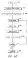
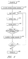
- FIGURE 1A illustrates one preferred embodiment of the dry plasma cleaning process.
- the CVD reactor is in standby mode.
- the CVD reactor is pre-cleaned by the in-situ oxygen plasma cleaning process.
- the first wafer is loaded into the CVD reactor in step 130, the desired film deposited thereon in step 140, and the wafer unloaded in step 150.
- the CVD reactor is cleaned with a remotely generated NF 3 -argon plasma. Steps 130-160 are repeated for the remaining wafers in the lot. After processing the last wafer, the CVD reactor is returned to standby mode in step 170.
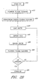
- FIGURE 1B illustrates a second preferred embodiment of the dry plasma cleaning process.
- the CVD reactor is in stand-by mode.
- the reactor is first cleaned with a remotely generated NF 3 -argon plasma.
- the reactor is pre-cleaned by the in-situ oxygen plasma cleaning process. Steps 215 and 220 may be performed in either order.
- the first wafer is loaded into the CVD reactor in step 230, the desired film deposited thereon in step 240, and the wafer unloaded in step 250.
- the CVD reactor is cleaned with a remotely generated NF 3 -argon plasma. Steps 230-260 are repeated for the remaining wafers in the lot. After processing the last wafer, the CVD reactor is returned to standby mode in step 270.
- FIGURE 2A illustrates a third preferred embodiment of the dry plasma cleaning process.
- the CVD reactor is in stand-by mode.
- the reactor is pre-cleaned by the downstream oxygen plasma cleaning process.
- the first wafer is loaded into the CVD reactor in step 330, the desired film deposited thereon in step 340, and the wafer unloaded in step 350.
- the CVD reactor is cleaned with a remotely generated NF 3 -argon plasma. Steps 330-360 are repeated for the remaining wafers in the lot.
- the CVD reactor is returned to standby mode in step 370.
- FIGURE 2B illustrates a fourth preferred embodiment of the dry plasma cleaning process.
- the CVD reactor is in stand-by mode.
- the CVD reactor is first cleaned with a remotely generated NF 3 -argon plasma.
- the reactor is pre-cleaned by the downstream O 2 plasma cleaning process. Steps 415 and 420 may be performed in either order.
- the first wafer is then loaded into the CVD reactor in step 430, the desired film deposited in step 440, and the wafer unloaded in step 450.
- step 460 the CVD reactor is cleaned with a remotely generated NF 3 -argon plasma. Steps 430-460 are repeated for the remaining wafers in the lot. After processing the last wafer, the CVD reactor is returned to standby mode in step 470.
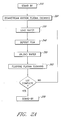
- FIGURE 3 illustrates a fifth preferred embodiment of the dry plasma cleaning process.
- the reactor is in stand-by mode.
- the reactor is cleaned by the downstream oxygen-fluorine plasma cleaning process.
- the first wafer is then loaded into the CVD reactor in step 530, the desired film deposited in step 540, and the wafer unloaded in step 550.
- the CVD reactor is cleaned either with a remotely generated NF 3 -argon plasma or by the downstream oxygen-fluorine plasma cleaning process. Steps 530-560 are repeated for the remaining wafers in the lot.
- the CVD reactor is returned to standby mode in step 570.
- a fluorine plasma cleaning of the CVD reaction chamber is not performed after the film deposition procedure for each wafer. Instead a fluorine plasma cleaning step is performed after film deposition on a predetermined number of wafers.
- the required frequency for the fluorine plasma cleaning step depends on the particular deposition conditions and its determination is within the scope of the skilled artisan without undue experimentation. Reducing the frequency of the fluorine plasma cleaning step improves the throughput of the CVD apparatus.
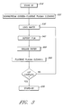
- step 610 the CVD reactor is in standby mode.
- step 620 the CVD reactor is pre-cleaned by the in-situ oxygen plasma cleaning process.
- the first wafer is loaded into the CVD reactor in step 630, the desired film deposited thereon in step 640, and the wafer unloaded in step 650.
- Steps 630-650 are repeated for a predetermined number of wafers.
- step 660 the CVD reactor is cleaned with a remotely generated NF 3 -argon plasma. Steps 630-660 are repeated for the remaining wafers in the lot. After processing the last wafer, the CVD reactor is returned to standby mode in step 670.
- FIGURE 5 illustrates a parallel-plate type plasma enhanced CVD apparatus in which the oxygen plasma cleaning process disclosed herein may be performed.
- the cleaning process may be also be performed in other types of CVD apparatus, for example, a reduced pressure thermal CVD apparatus.
- the CVD apparatus shown in FIGURE 5 is configured for providing a remotely generated plasma to the CVD processing chamber.
- a procedure for depositing a film on a semiconductor wafer in the apparatus shown in FIGURE 5 is performed as follows. After a stand-by period, one wafer 3 is placed within a transfer chamber 1. The wafer 3 is loaded onto a wafer support structure, or susceptor, 5 within a processing chamber 4 adjacent to a conveying chamber 1 by an auto transfer robot 2. The susceptor 5 also serves as an electrode equipped with a heater (heating element) 9 embedded therein. A reaction gas is evenly supplied onto the wafer 3 from a showerhead 6, which is parallel to the susceptor 5. Radio-frequency power is applied to the showerhead 6 by radio-frequency oscillators 7 and 7'. An RF matching system 12 is used between the radio-frequency oscillators 7 and 7', and the processing chamber 4.
- O 2 and He enter the CVD reactor through a gas line 13.
- the pressure in the reactor is controlled by the conductance control valve 8.
- RF power is turned on.
- RF power at 27 MHz dissociates the O 2 gas into reactive species.
- Reactive oxygen species with sufficient ion-bombardment energy will react with fluorine and carbon compounds deposited on the walls of reaction chamber 4 and the susceptor 5.
- the process converts non-volatile compounds into volatile compounds, which are then pumped out through the gate valve 8.
- the RF power, and the O 2 and He gases are automatically turned off.
- the conductance control valve 8 is opened fully to allow complete pump down of the entire reactor to remove the by-products.
- an inert gas such as argon is introduced into the remote plasma chamber 10 via the gas-line 14.
- the valve 11 is opened at the same time.
- the O 2 dissociates in the plasma chamber 10.
- the reactive cleaning species enter the CVD chamber through the valve 11. Reactive cleaning species with sufficient energy will remove fluorine and carbon compounds deposited on the walls of the reactor chamber 4 and the susceptor 5 by active species (e.g. , radical) assisted etching.
- This process converts these non-volatile compounds into volatile by-products, which are pumped out through the gate valve 8.
- the remote plasma unit 10 automatically turns off, followed by the flow of both the pre-mixed gas and the argon.
- the conductance control valve 8 is opened fully to allow the complete pump-down of the entire reactor to remove the by-products.
- a pre-mixed oxygen-containing gas for example O 2 mixed with argon
- O 2 oxygen-containing gas
- argon a pre-mixed oxygen-containing gas
- the valve 11 is opened at the same time.
- a fluorine-containing gas for example NF 3
- the gases dissociate in the plasma chamber 10.
- the reactive cleaning species enter the CVD plasma processing chamber 4 though the valve 11.
- the O 2 increases fluorine reactive species concentration by reducing fluorine ion recombination.
- the resulting plasma includes both reactive oxygen species and reactive fluorine species.
- Reactive cleaning species with sufficient energy will remove fluorine and carbon compounds deposited on the walls of the processing chamber 4 and the susceptor 5 by active species (e.g. , radical) assisted etching.
- active species e.g. , radical
- This process converts these non-volatile compounds into volatile by-products, which are pumped out through the gate valve 8.
- the remote plasma unit 10 After a pre-set "plasma on” time, the remote plasma unit 10 automatically turns off, followed by the flow of the gas sources.
- the conductance control valve 8 is opened fully to allow the complete pump-down of the entire reactor to remove the by-products.
- Exemplary downstream oxygen-fluorine plasma cleaning conditions are: NF 3 0.5-1 slm Argon 2-5 slm O 2 0.1-1.0 slm RF power (400 kHz) 2.0-2.8kW
- a mixed gas of Si(OCH 3 ) 2 (CH 3 ) 2 and helium is supplied as the reaction gas from the showerhead 6 to the processing chamber 4.
- the pressure within the processing chamber 4 is controlled and adjusted below about 1060 Pa using a conductance regulating valve 8 linked to the processing chamber 4.
- the heater 9 heats the susceptor 5 on which the wafer 3 is loaded.
- the wafer 3 is then heated to about 350-400 °C upon being loaded onto the susceptor 5.
- Radio-frequency power at 13.56 MHz, mixed power at 13.56 MHz and 430 MHz, power at 27.12MHz, or mixed power at 27.12MHz and 400kHz is applied between the susceptor 5 and the showerhead 6.
- the resulting plasma forms a thin film on the wafer 3.
- the wafer 3 is conveyed out of the processing chamber 4 by the auto transfer robot 2.
- mixtures of tetramethylsilane, Si(CH 3 ) 4 , or trimethylsilane, SiH(CH 3 ) 3 , and an oxygen-containing gas, for example O 2 , NO 2 , CO 2 , H 2 O, O 3 and mixtures thereof, may also be used as the reaction gas to deposit SiCO films.
- SiCO films are deposited on a batch of wafers by the method illustrated in FIGURE 2A.
- the downstream oxygen-fluorine plasma cleaning process described In EXAMPLE 1 is used in step 320.
- Plasma ignition of argon by radio-frequency power in a remote plasma discharge chamber 10 is followed by introducing a gas mixture of O 2 and NF 3 into remote the plasma discharge chamber 10. After the gases are disassociated and activated, they are brought into the processing chamber 4 through a valve 11, thereby cleaning the processing chamber 4.
- Film-deposition, step 340, and downstream fluorine cleaning, step 360, are performed alternately for each wafer in the lot.
- SiCO film deposition conditions are: Si (OCH 3 ) 2 (CH 3 ) 2 140 sccm Helium 50 sccm RF power (27.12 MHz) 1500-1650 W Pressure 560 Pa Electrode gap 24 mm Substrate temperature 370-380 °C
- Exemplary downstream fluorine plasma cleaning conditions are: NF 3 1 slm Argon 5 slm RF power (400 kHz) 2.1 - 2.8 kW
- SiC Silicon Carbide
- SiC films are used as hardmasks, as etch stop films for dual damascene dry etch processes, or as Cu diffusion barrier films.
- tetramethylsilane Si(CH 3 ) 4
- Si(CH 3 ) 4 is supplied to the CVD reactor instead of the Si(OCH 3 ) 2 (CH 3 ) 2 used in SiCO film deposition.
- a mixed gas of tetramethylsilane and helium is supplied as the reaction gas from the showerhead 6 to the processing chamber 4.
- the pressure in the processing chamber 4 is adjusted below about 1060 Pa using the conductance regulating valve 8.
- the heater 9 heats the susceptor 5 on which a wafer 3 is loaded.
- the wafer 3 is heated to about 300-380 °C upon being loaded onto the susceptor 5. Radio-frequency power at 13.56 MHz, mixed power at 13.56 MHz and 430 MHz, power at 27.12MHz, or mixed power at 27.12MHz and 400kHz is applied between the susceptor 5 and the showerhead 6. The resulting plasma deposits a thin film of SiC onto the wafer 3. After the thin film is formed, the wafer 3 is conveyed out of the processing chamber 4 by the auto transfer robot 2. In other embodiments, trimethylsilane (SiH(CH 3 ) 3 ) may also be used to deposit SiC films.
- SiH(CH 3 ) 3 trimethylsilane
- An oxygen poor SiCO film may also be used in place of a SiC film, and may be deposited by adding an oxygen-containing gas such as O 2 , NO 2 , CO 2 , O 3 , or mixtures thereof to the reaction gas mixture.
- an oxygen-containing gas such as O 2 , NO 2 , CO 2 , O 3 , or mixtures thereof.
- CO 2 is a preferred oxygen-containing gas for depositing such SiCO films.
- Silicon carbide films are deposited on a batch of wafers by the method illustrated in FIGURE 2A. Between deposition on each batch of wafers, the processing chamber 4 is cleaned in step 320 using the downstream oxygen-fluorine plasma cleaning process described in EXAMPLE 1. SiC film deposition, step 340, and downstream fluorine plasma cleaning, step 360, are alternately performed for each wafer in the batch. The downstream fluorine plasma cleaning is performed as described in EXAMPLE 2.
- SiC film deposition conditions are: Tetramethylsilane 200-700 sccm Helium 500-5000 sccm RF power (27.12 MHz) 300-1000 W RF power (400 kHz) 100-300 W Pressure 300-700 Pa Electrode gap 24 mm Substrate temperature 320-380 °C
- SiCN films may be used in place of silicon carbide films.
- An SiCN film may be deposited by adding a nitrogen-containing gas, for example NH 3 , to the deposition gas mixture.
Landscapes
- Chemical & Material Sciences (AREA)
- General Chemical & Material Sciences (AREA)
- Chemical Kinetics & Catalysis (AREA)
- Engineering & Computer Science (AREA)
- Materials Engineering (AREA)
- Mechanical Engineering (AREA)
- Metallurgy (AREA)
- Organic Chemistry (AREA)
- Chemical Vapour Deposition (AREA)
- Drying Of Semiconductors (AREA)
Applications Claiming Priority (2)
| Application Number | Priority Date | Filing Date | Title |
|---|---|---|---|
| US10/235,217 US6767836B2 (en) | 2002-09-04 | 2002-09-04 | Method of cleaning a CVD reaction chamber using an active oxygen species |
| US235217 | 2002-09-04 |
Publications (2)
| Publication Number | Publication Date |
|---|---|
| EP1452625A2 true EP1452625A2 (fr) | 2004-09-01 |
| EP1452625A3 EP1452625A3 (fr) | 2008-08-06 |
Family
ID=31977534
Family Applications (1)
| Application Number | Title | Priority Date | Filing Date |
|---|---|---|---|
| EP03019814A Withdrawn EP1452625A3 (fr) | 2002-09-04 | 2003-08-30 | Procédé de nettoyage d'une chambre de réaction CVD |
Country Status (4)
| Country | Link |
|---|---|
| US (1) | US6767836B2 (fr) |
| EP (1) | EP1452625A3 (fr) |
| JP (1) | JP4439860B2 (fr) |
| KR (1) | KR20040021533A (fr) |
Cited By (2)
| Publication number | Priority date | Publication date | Assignee | Title |
|---|---|---|---|---|
| EP1566468A3 (fr) * | 2004-02-18 | 2006-06-21 | Atmel Nantes Sa | Procédé pour la fabrication de circuits intégrés et dispositif correspondant. |
| EP4541932A1 (fr) * | 2023-10-16 | 2025-04-23 | SPTS Technologies Limited | Procédé de nettoyage d'un dispositif de traitement au plasma |
Families Citing this family (79)
| Publication number | Priority date | Publication date | Assignee | Title |
|---|---|---|---|---|
| US6875674B2 (en) * | 2000-07-10 | 2005-04-05 | Semiconductor Energy Laboratory Co., Ltd. | Method of manufacturing a semiconductor device with fluorine concentration |
| US20030005943A1 (en) * | 2001-05-04 | 2003-01-09 | Lam Research Corporation | High pressure wafer-less auto clean for etch applications |
| US20030110781A1 (en) | 2001-09-13 | 2003-06-19 | Zbigniew Zurecki | Apparatus and method of cryogenic cooling for high-energy cutting operations |
| US20030145694A1 (en) | 2002-02-04 | 2003-08-07 | Zbigniew Zurecki | Apparatus and method for machining of hard metals with reduced detrimental white layer effect |
| US7071129B2 (en) * | 2002-09-12 | 2006-07-04 | Intel Corporation | Enhancing adhesion of silicon nitride films to carbon-containing oxide films |
| US6932092B2 (en) * | 2002-11-22 | 2005-08-23 | Applied Materials, Inc. | Method for cleaning plasma enhanced chemical vapor deposition chamber using very high frequency energy |
| US7091133B2 (en) * | 2003-01-27 | 2006-08-15 | Asm Japan K.K. | Two-step formation of etch stop layer |
| JP2005033173A (ja) * | 2003-06-16 | 2005-02-03 | Renesas Technology Corp | 半導体集積回路装置の製造方法 |
| US6924239B2 (en) * | 2003-10-14 | 2005-08-02 | Texas Instruments Incorporated | Method for removal of hydrocarbon contamination on gate oxide prior to non-thermal nitridation using “spike” radical oxidation |
| US7419498B2 (en) * | 2003-10-21 | 2008-09-02 | Nmt Medical, Inc. | Quick release knot attachment system |
| JP2005142198A (ja) * | 2003-11-04 | 2005-06-02 | Taiyo Nippon Sanso Corp | クリーニングガス及びクリーニング方法 |
| US7354631B2 (en) * | 2003-11-06 | 2008-04-08 | Micron Technology, Inc. | Chemical vapor deposition apparatus and methods |
| KR100854809B1 (ko) * | 2003-11-11 | 2008-08-27 | 도쿄엘렉트론가부시키가이샤 | 기판 처리 방법과, 프로그램을 기록한 기억 매체 |
| US7267741B2 (en) * | 2003-11-14 | 2007-09-11 | Lam Research Corporation | Silicon carbide components of semiconductor substrate processing apparatuses treated to remove free-carbon |
| US7207339B2 (en) * | 2003-12-17 | 2007-04-24 | Taiwan Semiconductor Manufacturing Co., Ltd. | Method for cleaning a plasma enhanced CVD chamber |
| US20050155625A1 (en) * | 2004-01-20 | 2005-07-21 | Taiwan Semiconductor Manufacturing Co., Ltd. | Chamber cleaning method |
| WO2005081302A1 (fr) * | 2004-02-19 | 2005-09-01 | Tokyo Electron Limited | Procédé de nettoyage d'une chambre de traitement dans un appareil de traitement de substrat et procédé de détection de la fin du nettoyage |
| US20050258137A1 (en) * | 2004-03-24 | 2005-11-24 | Sawin Herbert H | Remote chamber methods for removing surface deposits |
| US7513121B2 (en) | 2004-03-25 | 2009-04-07 | Air Products And Chemicals, Inc. | Apparatus and method for improving work surface during forming and shaping of materials |
| US20070286965A1 (en) * | 2006-06-08 | 2007-12-13 | Martin Jay Seamons | Methods for the reduction and elimination of particulate contamination with cvd of amorphous carbon |
| CN100461344C (zh) * | 2004-07-23 | 2009-02-11 | 气体产品与化学公司 | 从基板上清除含碳的残余物的方法 |
| US7581549B2 (en) * | 2004-07-23 | 2009-09-01 | Air Products And Chemicals, Inc. | Method for removing carbon-containing residues from a substrate |
| US20060054183A1 (en) * | 2004-08-27 | 2006-03-16 | Thomas Nowak | Method to reduce plasma damage during cleaning of semiconductor wafer processing chamber |
| US7819981B2 (en) * | 2004-10-26 | 2010-10-26 | Advanced Technology Materials, Inc. | Methods for cleaning ion implanter components |
| US7291286B2 (en) * | 2004-12-23 | 2007-11-06 | Lam Research Corporation | Methods for removing black silicon and black silicon carbide from surfaces of silicon and silicon carbide electrodes for plasma processing apparatuses |
| US20060144819A1 (en) * | 2004-12-30 | 2006-07-06 | Sawin Herbert H | Remote chamber methods for removing surface deposits |
| US20060144820A1 (en) * | 2004-12-30 | 2006-07-06 | Sawin Herbert H | Remote chamber methods for removing surface deposits |
| US20070006893A1 (en) * | 2005-07-08 | 2007-01-11 | Bing Ji | Free radical initiator in remote plasma chamber clean |
| TW200718479A (en) * | 2005-08-02 | 2007-05-16 | Massachusetts Inst Technology | Method of using sulfur fluoride for removing surface deposits |
| CN101278072A (zh) * | 2005-08-02 | 2008-10-01 | 麻省理工学院 | 使用nf3除去表面沉积物的方法 |
| US7434439B2 (en) | 2005-10-14 | 2008-10-14 | Air Products And Chemicals, Inc. | Cryofluid assisted forming method |
| US7390240B2 (en) | 2005-10-14 | 2008-06-24 | Air Products And Chemicals, Inc. | Method of shaping and forming work materials |
| KR100727259B1 (ko) * | 2005-12-29 | 2007-06-11 | 동부일렉트로닉스 주식회사 | 반도체 장치의 배선 형성방법 |
| US8057603B2 (en) * | 2006-02-13 | 2011-11-15 | Tokyo Electron Limited | Method of cleaning substrate processing chamber, storage medium, and substrate processing chamber |
| US20070207275A1 (en) * | 2006-02-21 | 2007-09-06 | Applied Materials, Inc. | Enhancement of remote plasma source clean for dielectric films |
| US20070248767A1 (en) * | 2006-04-19 | 2007-10-25 | Asm Japan K.K. | Method of self-cleaning of carbon-based film |
| KR101467585B1 (ko) | 2006-04-26 | 2014-12-01 | 어드밴스드 테크놀러지 머티리얼즈, 인코포레이티드 | 반도체 공정 시스템의 세정 |
| US20080083701A1 (en) * | 2006-10-04 | 2008-04-10 | Mks Instruments, Inc. | Oxygen conditioning of plasma vessels |
| US7550090B2 (en) * | 2007-01-23 | 2009-06-23 | Applied Materials, Inc. | Oxygen plasma clean to remove carbon species deposited on a glass dome surface |
| TWI424105B (zh) * | 2007-05-14 | 2014-01-21 | 東京威力科創股份有限公司 | 成膜裝置及使用其之方法 |
| US20080299775A1 (en) * | 2007-06-04 | 2008-12-04 | Applied Materials, Inc. | Gapfill extension of hdp-cvd integrated process modulation sio2 process |
| US7867921B2 (en) * | 2007-09-07 | 2011-01-11 | Applied Materials, Inc. | Reduction of etch-rate drift in HDP processes |
| US7745350B2 (en) * | 2007-09-07 | 2010-06-29 | Applied Materials, Inc. | Impurity control in HDP-CVD DEP/ETCH/DEP processes |
| US20090090382A1 (en) * | 2007-10-05 | 2009-04-09 | Asm Japan K.K. | Method of self-cleaning of carbon-based film |
| US20090114245A1 (en) * | 2007-11-02 | 2009-05-07 | Hidehiro Kojiri | In-situ chamber cleaning method |
| SG188150A1 (en) | 2008-02-11 | 2013-03-28 | Advanced Tech Materials | Ion source cleaning in semiconductor processing systems |
| US8262800B1 (en) | 2008-02-12 | 2012-09-11 | Novellus Systems, Inc. | Methods and apparatus for cleaning deposition reactors |
| US7972968B2 (en) * | 2008-08-18 | 2011-07-05 | Applied Materials, Inc. | High density plasma gapfill deposition-etch-deposition process etchant |
| JP2010047818A (ja) * | 2008-08-25 | 2010-03-04 | Toshiba Corp | 半導体製造装置および半導体製造方法 |
| US8404135B2 (en) * | 2008-08-26 | 2013-03-26 | Taiwan Semiconductor Manufacturing Co., Ltd. | Plasma cleaning for process chamber component refurbishment |
| US20100104770A1 (en) * | 2008-10-27 | 2010-04-29 | Asm Japan K.K. | Two-step formation of hydrocarbon-based polymer film |
| US8591659B1 (en) | 2009-01-16 | 2013-11-26 | Novellus Systems, Inc. | Plasma clean method for deposition chamber |
| CN102597309A (zh) * | 2009-10-30 | 2012-07-18 | 苏威氟有限公司 | 去除沉积物的方法 |
| JP5421736B2 (ja) * | 2009-11-13 | 2014-02-19 | 株式会社日立国際電気 | 半導体装置の製造方法、基板処理装置、及びプログラム |
| US8247332B2 (en) * | 2009-12-04 | 2012-08-21 | Novellus Systems, Inc. | Hardmask materials |
| US8497211B2 (en) | 2011-06-24 | 2013-07-30 | Applied Materials, Inc. | Integrated process modulation for PSG gapfill |
| US20130133697A1 (en) * | 2011-06-29 | 2013-05-30 | Paul A. STOCKMAN | Prevention of post-pecvd vacuum and abatement system fouling using a fluorine containing cleaning gas chamber |
| DE102011056538A1 (de) * | 2011-12-16 | 2013-06-20 | Aixtron Se | Verfahren zum Entfernen unerwünschter Rückstände aus einem MOCVD-Reaktor sowie zugehörige Vorrichtung |
| US10325773B2 (en) | 2012-06-12 | 2019-06-18 | Novellus Systems, Inc. | Conformal deposition of silicon carbide films |
| US9234276B2 (en) | 2013-05-31 | 2016-01-12 | Novellus Systems, Inc. | Method to obtain SiC class of films of desired composition and film properties |
| US10832904B2 (en) | 2012-06-12 | 2020-11-10 | Lam Research Corporation | Remote plasma based deposition of oxygen doped silicon carbide films |
| US10211310B2 (en) | 2012-06-12 | 2019-02-19 | Novellus Systems, Inc. | Remote plasma based deposition of SiOC class of films |
| US9337068B2 (en) | 2012-12-18 | 2016-05-10 | Lam Research Corporation | Oxygen-containing ceramic hard masks and associated wet-cleans |
| US9018108B2 (en) | 2013-01-25 | 2015-04-28 | Applied Materials, Inc. | Low shrinkage dielectric films |
| US10297442B2 (en) | 2013-05-31 | 2019-05-21 | Lam Research Corporation | Remote plasma based deposition of graded or multi-layered silicon carbide film |
| US20160314964A1 (en) | 2015-04-21 | 2016-10-27 | Lam Research Corporation | Gap fill using carbon-based films |
| US9601319B1 (en) * | 2016-01-07 | 2017-03-21 | Lam Research Corporation | Systems and methods for eliminating flourine residue in a substrate processing chamber using a plasma-based process |
| US9847221B1 (en) | 2016-09-29 | 2017-12-19 | Lam Research Corporation | Low temperature formation of high quality silicon oxide films in semiconductor device manufacturing |
| US10049869B2 (en) * | 2016-09-30 | 2018-08-14 | Lam Research Corporation | Composite dielectric interface layers for interconnect structures |
| US10002787B2 (en) | 2016-11-23 | 2018-06-19 | Lam Research Corporation | Staircase encapsulation in 3D NAND fabrication |
| CN106756765B (zh) * | 2016-11-30 | 2019-06-25 | 东北大学 | 一种金属材料表面含氟抗菌涂层及其制备方法 |
| US9837270B1 (en) | 2016-12-16 | 2017-12-05 | Lam Research Corporation | Densification of silicon carbide film using remote plasma treatment |
| WO2020045663A1 (fr) * | 2018-08-31 | 2020-03-05 | 日本特殊コーティング株式会社 | Composition de résine durcissable par rayonnement |
| CN111112267B (zh) * | 2019-12-24 | 2022-09-02 | 西安奕斯伟材料科技有限公司 | 一种气相沉积反应腔体的清洗装置、清洗系统及清洗方法 |
| KR20210137395A (ko) | 2020-05-07 | 2021-11-17 | 에이에스엠 아이피 홀딩 비.브이. | 불소계 라디칼을 이용하여 반응 챔버의 인시츄 식각을 수행하기 위한 장치 및 방법 |
| CN111599706A (zh) * | 2020-05-26 | 2020-08-28 | 上海华虹宏力半导体制造有限公司 | 在线侦测腔体漏率的方法、半导体工艺机台 |
| US20220178017A1 (en) * | 2020-12-03 | 2022-06-09 | Applied Materials, Inc. | Cfx layer to protect aluminum surface from over-oxidation |
| US20230069139A1 (en) * | 2021-08-30 | 2023-03-02 | Asm Ip Holding B.V. | Cvd apparatus and method for cleaning chamber of cvd apparatus |
| KR20230100631A (ko) | 2021-12-28 | 2023-07-05 | 에이에스엠 아이피 홀딩 비.브이. | 고주파 전력을 갖는 저 유전율 재료 층을 형성하는 방법, 상기 층을 포함하는 구조, 및 이를 형성하기 위한 시스템 |
Family Cites Families (25)
| Publication number | Priority date | Publication date | Assignee | Title |
|---|---|---|---|---|
| JPH03183125A (ja) * | 1983-09-22 | 1991-08-09 | Semiconductor Energy Lab Co Ltd | プラズマ気相反応方法 |
| JPS61250185A (ja) * | 1985-04-25 | 1986-11-07 | Anelva Corp | 真空処理装置のクリ−ニング方法 |
| JPS63210275A (ja) * | 1987-02-24 | 1988-08-31 | Semiconductor Energy Lab Co Ltd | プラズマ反応装置内を清浄にする方法 |
| US5176791A (en) * | 1988-08-11 | 1993-01-05 | Semiconductor Energy Laboratory Co., Ltd. | Method for forming carbonaceous films |
| DE4202158C1 (fr) * | 1992-01-27 | 1993-07-22 | Siemens Ag, 8000 Muenchen, De | |
| US5417826A (en) * | 1992-06-15 | 1995-05-23 | Micron Technology, Inc. | Removal of carbon-based polymer residues with ozone, useful in the cleaning of plasma reactors |
| JP3502096B2 (ja) * | 1992-06-22 | 2004-03-02 | ラム リサーチ コーポレイション | プラズマ処理装置内の残留物を除去するためのプラズマクリーニング方法 |
| US5252178A (en) * | 1992-06-24 | 1993-10-12 | Texas Instruments Incorporated | Multi-zone plasma processing method and apparatus |
| JP3175117B2 (ja) * | 1993-05-24 | 2001-06-11 | 東京エレクトロン株式会社 | ドライクリーニング方法 |
| US5756400A (en) * | 1995-12-08 | 1998-05-26 | Applied Materials, Inc. | Method and apparatus for cleaning by-products from plasma chamber surfaces |
| US6347636B1 (en) | 1996-11-13 | 2002-02-19 | Applied Materials, Inc. | Methods and apparatus for gettering fluorine from chamber material surfaces |
| US6026762A (en) | 1997-04-23 | 2000-02-22 | Applied Materials, Inc. | Apparatus for improved remote microwave plasma source for use with substrate processing systems |
| US6077572A (en) * | 1997-06-18 | 2000-06-20 | Northeastern University | Method of coating edges with diamond-like carbon |
| US5981000A (en) * | 1997-10-14 | 1999-11-09 | International Business Machines Corporation | Method for fabricating a thermally stable diamond-like carbon film |
| US6383955B1 (en) | 1998-02-05 | 2002-05-07 | Asm Japan K.K. | Silicone polymer insulation film on semiconductor substrate and method for forming the film |
| TW437017B (en) | 1998-02-05 | 2001-05-28 | Asm Japan Kk | Silicone polymer insulation film on semiconductor substrate and method for formation thereof |
| US6374831B1 (en) | 1999-02-04 | 2002-04-23 | Applied Materials, Inc. | Accelerated plasma clean |
| SG101418A1 (en) * | 1999-03-30 | 2004-01-30 | Showa Denko Kk | Production process for magnetic recording medium |
| JP3072989B1 (ja) | 1999-05-14 | 2000-08-07 | 日本エー・エス・エム株式会社 | 半導体基板上に薄膜を形成する成膜装置における成膜方法 |
| US6255222B1 (en) * | 1999-08-24 | 2001-07-03 | Applied Materials, Inc. | Method for removing residue from substrate processing chamber exhaust line for silicon-oxygen-carbon deposition process |
| KR100767762B1 (ko) | 2000-01-18 | 2007-10-17 | 에이에스엠 저펜 가부시기가이샤 | 자가 세정을 위한 원격 플라즈마 소스를 구비한 cvd 반도체 공정장치 |
| US6329297B1 (en) | 2000-04-21 | 2001-12-11 | Applied Materials, Inc. | Dilute remote plasma clean |
| US6387207B1 (en) | 2000-04-28 | 2002-05-14 | Applied Materials, Inc. | Integration of remote plasma generator with semiconductor processing chamber |
| US6569257B1 (en) * | 2000-11-09 | 2003-05-27 | Applied Materials Inc. | Method for cleaning a process chamber |
| JP2002198370A (ja) * | 2000-12-26 | 2002-07-12 | Mitsubishi Electric Corp | 半導体装置および半導体装置の製造方法 |
-
2002
- 2002-09-04 US US10/235,217 patent/US6767836B2/en not_active Expired - Lifetime
-
2003
- 2003-08-25 KR KR1020030058753A patent/KR20040021533A/ko not_active Withdrawn
- 2003-08-30 EP EP03019814A patent/EP1452625A3/fr not_active Withdrawn
- 2003-09-04 JP JP2003312924A patent/JP4439860B2/ja not_active Expired - Lifetime
Cited By (2)
| Publication number | Priority date | Publication date | Assignee | Title |
|---|---|---|---|---|
| EP1566468A3 (fr) * | 2004-02-18 | 2006-06-21 | Atmel Nantes Sa | Procédé pour la fabrication de circuits intégrés et dispositif correspondant. |
| EP4541932A1 (fr) * | 2023-10-16 | 2025-04-23 | SPTS Technologies Limited | Procédé de nettoyage d'un dispositif de traitement au plasma |
Also Published As
| Publication number | Publication date |
|---|---|
| JP2004134766A (ja) | 2004-04-30 |
| EP1452625A3 (fr) | 2008-08-06 |
| KR20040021533A (ko) | 2004-03-10 |
| JP4439860B2 (ja) | 2010-03-24 |
| US6767836B2 (en) | 2004-07-27 |
| US20040043626A1 (en) | 2004-03-04 |
Similar Documents
| Publication | Publication Date | Title |
|---|---|---|
| US6767836B2 (en) | Method of cleaning a CVD reaction chamber using an active oxygen species | |
| US6071573A (en) | Process for precoating plasma CVD reactors | |
| US6274058B1 (en) | Remote plasma cleaning method for processing chambers | |
| US6569257B1 (en) | Method for cleaning a process chamber | |
| JP3090476B2 (ja) | プラズマ化学蒸着を用いてフッ化シリコン酸化物層を形成する方法 | |
| US6846742B2 (en) | Si seasoning to reduce particles, extend clean frequency, block mobile ions and increase chamber throughput | |
| US7288284B2 (en) | Post-cleaning chamber seasoning method | |
| US7144606B2 (en) | Plasma treatment to enhance adhesion and to minimize oxidation of carbon-containing layers | |
| US5354715A (en) | Thermal chemical vapor deposition of silicon dioxide and in-situ multi-step planarized process | |
| EP0665583A2 (fr) | Méthode d'attaque de couches de nitrure de titane et d'oxyde isolant utilisant un gaz comprenant du fluoride de carbone et de l'oxyde de carbone | |
| US5919336A (en) | Apparatus for fabricating semiconductor device and method for fabricating semiconductor device | |
| US6777171B2 (en) | Fluorine-containing layers for damascene structures | |
| US20050178333A1 (en) | System and method of CVD chamber cleaning | |
| EP0936282A2 (fr) | Diélectrique en carbone amorphe fluoré présentant une constante diélectrique (k) faible, et sa méthode de fabrication | |
| US20030143410A1 (en) | Method for reduction of contaminants in amorphous-silicon film | |
| US20060093756A1 (en) | High-power dielectric seasoning for stable wafer-to-wafer thickness uniformity of dielectric CVD films | |
| US20010033900A1 (en) | Nitrogen treatment of polished halogen-doped silicon glass | |
| US20050155625A1 (en) | Chamber cleaning method | |
| US7207339B2 (en) | Method for cleaning a plasma enhanced CVD chamber | |
| US20140272184A1 (en) | Methods for maintaining clean etch rate and reducing particulate contamination with pecvd of amorphous silicon filims | |
| US8084088B2 (en) | Method of improving the wafer-to-wafer thickness uniformity of silicon nitride layers | |
| US6413887B1 (en) | Method for producing silicon nitride series film | |
| US20220301887A1 (en) | Ruthenium etching process | |
| US6749717B1 (en) | Device for in-situ cleaning of an inductively-coupled plasma chambers | |
| US5281557A (en) | Soluble oxides for integrated circuit fabrication formed by the incomplete dissociation of the precursor gas |
Legal Events
| Date | Code | Title | Description |
|---|---|---|---|
| PUAI | Public reference made under article 153(3) epc to a published international application that has entered the european phase |
Free format text: ORIGINAL CODE: 0009012 |
|
| AK | Designated contracting states |
Kind code of ref document: A2 Designated state(s): AT BE BG CH CY CZ DE DK EE ES FI FR GB GR HU IE IT LI LU MC NL PT RO SE SI SK TR |
|
| AX | Request for extension of the european patent |
Extension state: AL LT LV MK |
|
| PUAL | Search report despatched |
Free format text: ORIGINAL CODE: 0009013 |
|
| AK | Designated contracting states |
Kind code of ref document: A3 Designated state(s): AT BE BG CH CY CZ DE DK EE ES FI FR GB GR HU IE IT LI LU MC NL PT RO SE SI SK TR |
|
| AX | Request for extension of the european patent |
Extension state: AL LT LV MK |
|
| AKX | Designation fees paid | ||
| STAA | Information on the status of an ep patent application or granted ep patent |
Free format text: STATUS: THE APPLICATION IS DEEMED TO BE WITHDRAWN |
|
| 18D | Application deemed to be withdrawn |
Effective date: 20090207 |
|
| REG | Reference to a national code |
Ref country code: DE Ref legal event code: 8566 |