EP1453062B1 - Méthode de test intégré dans une mémoire Flash - Google Patents
Méthode de test intégré dans une mémoire Flash Download PDFInfo
- Publication number
- EP1453062B1 EP1453062B1 EP03425126A EP03425126A EP1453062B1 EP 1453062 B1 EP1453062 B1 EP 1453062B1 EP 03425126 A EP03425126 A EP 03425126A EP 03425126 A EP03425126 A EP 03425126A EP 1453062 B1 EP1453062 B1 EP 1453062B1
- Authority
- EP
- European Patent Office
- Prior art keywords
- cache
- address
- counter
- memory
- redundancy
- Prior art date
- Legal status (The legal status is an assumption and is not a legal conclusion. Google has not performed a legal analysis and makes no representation as to the accuracy of the status listed.)
- Expired - Lifetime
Links
- 238000012360 testing method Methods 0.000 title claims description 104
- 230000015654 memory Effects 0.000 title claims description 69
- 238000000034 method Methods 0.000 title description 16
- 239000013598 vector Substances 0.000 claims description 30
- 238000004458 analytical method Methods 0.000 claims description 17
- 238000010200 validation analysis Methods 0.000 claims description 5
- 230000008878 coupling Effects 0.000 claims 1
- 238000010168 coupling process Methods 0.000 claims 1
- 238000005859 coupling reaction Methods 0.000 claims 1
- 230000006386 memory function Effects 0.000 claims 1
- VLCQZHSMCYCDJL-UHFFFAOYSA-N tribenuron methyl Chemical compound COC(=O)C1=CC=CC=C1S(=O)(=O)NC(=O)N(C)C1=NC(C)=NC(OC)=N1 VLCQZHSMCYCDJL-UHFFFAOYSA-N 0.000 claims 1
- 238000005259 measurement Methods 0.000 description 20
- 238000010586 diagram Methods 0.000 description 15
- 230000006870 function Effects 0.000 description 11
- 238000013459 approach Methods 0.000 description 10
- 239000011159 matrix material Substances 0.000 description 8
- 238000004519 manufacturing process Methods 0.000 description 7
- 230000008569 process Effects 0.000 description 6
- 230000008439 repair process Effects 0.000 description 6
- 238000013461 design Methods 0.000 description 5
- XUIMIQQOPSSXEZ-UHFFFAOYSA-N Silicon Chemical compound [Si] XUIMIQQOPSSXEZ-UHFFFAOYSA-N 0.000 description 4
- 230000007547 defect Effects 0.000 description 4
- 238000001514 detection method Methods 0.000 description 4
- 230000018109 developmental process Effects 0.000 description 4
- 238000005516 engineering process Methods 0.000 description 4
- 229910052710 silicon Inorganic materials 0.000 description 4
- 239000010703 silicon Substances 0.000 description 4
- 230000008901 benefit Effects 0.000 description 3
- 230000008859 change Effects 0.000 description 3
- 230000007246 mechanism Effects 0.000 description 3
- 238000009966 trimming Methods 0.000 description 3
- 102100022103 Histone-lysine N-methyltransferase 2A Human genes 0.000 description 2
- 101001045846 Homo sapiens Histone-lysine N-methyltransferase 2A Proteins 0.000 description 2
- 238000004364 calculation method Methods 0.000 description 2
- 238000011161 development Methods 0.000 description 2
- 230000001965 increasing effect Effects 0.000 description 2
- PWPJGUXAGUPAHP-UHFFFAOYSA-N lufenuron Chemical compound C1=C(Cl)C(OC(F)(F)C(C(F)(F)F)F)=CC(Cl)=C1NC(=O)NC(=O)C1=C(F)C=CC=C1F PWPJGUXAGUPAHP-UHFFFAOYSA-N 0.000 description 2
- 239000002184 metal Substances 0.000 description 2
- 230000009467 reduction Effects 0.000 description 2
- 238000011160 research Methods 0.000 description 2
- 208000013641 Cerebrofacial arteriovenous metameric syndrome Diseases 0.000 description 1
- 238000010521 absorption reaction Methods 0.000 description 1
- 230000003213 activating effect Effects 0.000 description 1
- 230000033228 biological regulation Effects 0.000 description 1
- 230000005540 biological transmission Effects 0.000 description 1
- 230000011712 cell development Effects 0.000 description 1
- 238000012512 characterization method Methods 0.000 description 1
- 230000000295 complement effect Effects 0.000 description 1
- 230000006835 compression Effects 0.000 description 1
- 238000007906 compression Methods 0.000 description 1
- 230000003750 conditioning effect Effects 0.000 description 1
- 230000003247 decreasing effect Effects 0.000 description 1
- 230000001934 delay Effects 0.000 description 1
- 230000001419 dependent effect Effects 0.000 description 1
- 230000009977 dual effect Effects 0.000 description 1
- 230000008030 elimination Effects 0.000 description 1
- 238000003379 elimination reaction Methods 0.000 description 1
- 230000002708 enhancing effect Effects 0.000 description 1
- 238000011990 functional testing Methods 0.000 description 1
- 230000000977 initiatory effect Effects 0.000 description 1
- 230000014759 maintenance of location Effects 0.000 description 1
- 238000007726 management method Methods 0.000 description 1
- 238000000691 measurement method Methods 0.000 description 1
- 238000012797 qualification Methods 0.000 description 1
- 230000001105 regulatory effect Effects 0.000 description 1
- 238000012827 research and development Methods 0.000 description 1
- 239000000523 sample Substances 0.000 description 1
- 238000010845 search algorithm Methods 0.000 description 1
- 239000004065 semiconductor Substances 0.000 description 1
- 230000011664 signaling Effects 0.000 description 1
- 238000012795 verification Methods 0.000 description 1
Images












Classifications
-
- G—PHYSICS
- G11—INFORMATION STORAGE
- G11C—STATIC STORES
- G11C29/00—Checking stores for correct operation ; Subsequent repair; Testing stores during standby or offline operation
- G11C29/04—Detection or location of defective memory elements, e.g. cell constructio details, timing of test signals
- G11C29/08—Functional testing, e.g. testing during refresh, power-on self testing [POST] or distributed testing
- G11C29/12—Built-in arrangements for testing, e.g. built-in self testing [BIST] or interconnection details
- G11C29/14—Implementation of control logic, e.g. test mode decoders
- G11C29/16—Implementation of control logic, e.g. test mode decoders using microprogrammed units, e.g. state machines
-
- G—PHYSICS
- G11—INFORMATION STORAGE
- G11C—STATIC STORES
- G11C16/00—Erasable programmable read-only memories
- G11C16/02—Erasable programmable read-only memories electrically programmable
- G11C16/04—Erasable programmable read-only memories electrically programmable using variable threshold transistors, e.g. FAMOS
-
- G—PHYSICS
- G11—INFORMATION STORAGE
- G11C—STATIC STORES
- G11C29/00—Checking stores for correct operation ; Subsequent repair; Testing stores during standby or offline operation
- G11C29/04—Detection or location of defective memory elements, e.g. cell constructio details, timing of test signals
- G11C2029/0401—Detection or location of defective memory elements, e.g. cell constructio details, timing of test signals in embedded memories
-
- G—PHYSICS
- G11—INFORMATION STORAGE
- G11C—STATIC STORES
- G11C29/00—Checking stores for correct operation ; Subsequent repair; Testing stores during standby or offline operation
- G11C29/04—Detection or location of defective memory elements, e.g. cell constructio details, timing of test signals
- G11C2029/0405—Detection or location of defective memory elements, e.g. cell constructio details, timing of test signals comprising complete test loop
Definitions
- This invention relates in general to the fabrication of integrated digital devices and in particular to the techniques of quality test, configuration, repair and validation of memory devices that are carried out at wafer level during the fabrication process.
- the speeding up of the industrialization phase and optimizing test strategy for timely achieve validation and qualification of devices involve several factors such as: right choice of the testing platform and of the level of test coverage, built-in self-test, device setting and repair techniques.
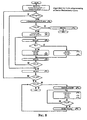
- Electrical Wafer Sort is a sequence of test routines carried out on the wafer before and after a baking step, according to the following flow.
- the tests performed during EWS can be classified in the following groups:
- Testing machines are also expensive. Both the software and the testing hardware have a cost that is commensurate to the complexity and numerosity of tests that must be performed according to the EWS flow to achieve the acceptable reliability. In case of memory devices, the impact that a single routine has on the global time requested to fully test a device depends to a large measure to the size of the memory array.
- the main test routines that may be executed via built-in test are:
- DIMM Dual In-line Memory Modules
- Each DIMM comprises an Electrically Erasable Read Only Memory (EEPROM) for storing configuration and error management information used by the microcontroller.
- EEPROM Electrically Erasable Read Only Memory
- the microcontroller reads each EPPROM for configuration information and stores this information in its local RAM.
- the microcontroller manages the DIMMs by initiating Built-In Self Tests and retrieving the status of the tests to identify a failed DIMM.
- the invention is defined by a memory memory device according to claim 1.
- the architecture of this invention gives the possibility of executing the above-listed routines internally without involving any external complex or expensive test equipment to control the test program.
- the algorithms are executed by the onboard micro-controllers (that may be reading either from an embedded ROM or from a GLOBAL CACHE purposely provided).
- Such a GLOBAL CACHE may be downloaded with the desired routine to a TUI block and provides a full test flexibility also at device debug level.
- Managing test routines by an internal algorithm permits to make the device architecture transparent from a tester point of view, by purposely creating a standard interface with a set of defined commands and instructions to be interpreted by the on board micro and internally executed.
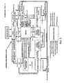
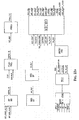
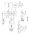
- the in-built system according to the present invention is based on an architecture, a high level diagram of which is depicted in Figure 2.
- Identification of fail cells is done by scanning the memory locations of the sectors and by comparing the read datum with the expected one.
- the scanning is done by column, incrementing the row address between a read operation and the next.
- Redundancy analysis which is carried out from one sector at the time is added.
- the number of resources already used for the sector to be analyzed is read from GLOBAL CACHE. This information is loaded in the RESOURCE COUNTER through the control signal LOAD_RS_LATCH and LOAD_RS_CNT. Of course, if the sector has been analyzed for the first time, the number of resources already used is equal to 0.
- Access to the first field of the GLOBAL_CACHE, containing the number of resources already used for the sector under analysis, is obtained by reading the GLOBAL_CACHE by the signal READ_GLB, after having forced the signal FORCE_ZERO_OFFSET.
- the column address is incremented and the next column is scanned.
- the RESOURCE COUNTER When all the sector has been scanned, in the RESOURCE COUNTER will be present the total number of resources necessary for preparing the sector. This is equal to the sum of the number of resources already used before the last redundancy analysis of the sector and of all necessary for preparing the fails detected during the last scanning.
- the MICRO writes in the GLOBAL CACHE the total number of resources used for the sector in question, the column addresses at which failures have been found an the position of the failed physical columns.
- the content of the RESOURCE COUNTER is compared with the content that the same counter had before starting the new scanning, stored in the LATCH of the RESOURCE_COUNTER. If the two value are equal (EOU is active), there didn't been new failure and the content of the GLOBAL CACHE does not need updating. On the contrary, if the value contains in the RESOURCE COUNTER is greater than the one stored before the scanning, new failures have occurs that must therefore be added to the failures already recorded in the GLOBAL CACHE. In the latter case is therefore necessary to store these new failures within the GLOBAL CACHE.
- the new value is used as pointer to the GLOBAL CACHE (combined with the sector address), to the LOCAL DATA CACHE and to the LOCAL ADDRESS CACHE.
- the BIT POSITION COUNTER is also reset.
- the register of the LOCAL DATA CACHE pointed by the RESOURCE_ADD is scanned bit by bit until a bit fail is found. While this scanning takes place, the BIT POSITION COUNTER is incremented. As soon as a bit fail is found, the column address has reached a fail has been detected (contain in the LOCAL ADDRESS CACHE) and its location (contain in the BIT POSITION COUNTER) are written in sequence in the GLOBAL CACHE.
- the RESOURCE COUNTER is decrement.
- bit by bit scanning is continued from the point in which it was interrupted and these other bit fails are stored in the GLOBAL CACHE.
- the BIT POSITION COUNTER is reset and a new scanning starts and so forced until the value of the resource counter coincides with the starting value (EOU becomes active) and therefore until all new bit fail that have been found having recorded in the GLOBAL CACHE.
- the information on the basis of which the redundancy cams may be properly programmed are available. This information is stored within the GLOBAL CACHE and is organized in records.
- Each record is associated to one specific sector and is formed by a certain number of fields.
- the first of these fields contains the number of column redundancy used for the specific sector.
- the following fields contain the information necessary for identify the address of columns to be redundant and to the sense amplifiers to which they pertain.
- the last field of each record indicates whether the sector in question is to be fully redundant by sector redundancy.
- redundancy vectors that is the vectors to be programmed for sector redundancy and in the cams to be programmed for column redundancy.
- the sector redundancy vectors all of this contain two fields: the guard bit and the address of the sector to be redundant.
- the column redundancy vectors contain three fields: the guard bit, the address corresponding to the column to be redundant and the sense amplifier to which such a column pertains.
- redundancy cams belonging to a same vector occupy adjacent topological positions, that are addressable by topologically consecutive addresses, generally column addresses. Moreover, the same vectors are in their turn topologically consecutive to another.
- Each cam is composed of two groups of flash cells, connected to the two side of a latch.
- each group of flash cells be composed of a single cell.
- the setting of a cam equals programming the flash cells connected to one only of the two side of the latch.
- the latch will imbalance itself to one of the two permitted stable states.
- the programming of the redundancy vectors consists in programming in succession the corresponding cam vectors.
- the bit of the corresponding cams are all set to 1.
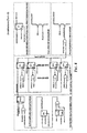
- the architecture that is used for the automatic programming of the cams and for carrying out the algorithms of sector and column redundancy programming of the cams employs:
- the sector redundancy cams are commonly organized within an array of a single row and a number of column equal to: N ⁇ Z ⁇ 2 where N is the number of sector redundancy sources available, Z is the number of bit contained in each sector redundancy vector (equal to the number of bits of the sector address + 1 bit because of the presence of a guard bit) and 2 is the multiplier accounting for the fact that each cam is composed of two cells (one connected to the left side and the other to the right side of the latch).
- a sector redundancy vectors contains a first field composed of a single guard bit (which is 0 if the redundancy resource is used or 1 if on the contrary the resource is unused) and a second field in which the fail sector address is stored.
- the programming algorithm of the sector redundancy cams starts, after a global reset of the system, with the enabling of the signal SECTOR_REPAIR_ACTIVE. This is done in order to select the access path to the REDUNDACY_REGISTER that permits the input of a "0" on the guard bit and of the sector address bits in the remaining bits.
- the next step is the setting to "1" the signal FORCE_MAX_OFFSET, in order to point within the global cache to the last field, that is the field that informs whether the sector currently addressed through the DEVICE_ADDRESS_COUNTER is a failed sector or not.
- the sector If the sector is not failed, it will not need to be redundant and the analysis passes to the following sectors. On the contrary, if the sector is failed it will need to be redundant.
- the RESOURCE_COUNTER is incremented an d a check is made to establish whether the number of redundancy resources required so far is larger to the number of available resources. In which case the algorithm sets a fail and exit.
- the sector redundancy vector that must be recorded in the cams is loaded in the REDUNDANCY_REGISTER by enabling the signal LOAD_RED_COUNTER, which it should be record points to one of the bits of the REDUNDANCY_REGISTER, follows.
- the bit of the REDUNDANCY_REGISTER are read one at the time and depending on the value the cams are properly programmed.
- the scanning of the cams within the array of sector redundancy cams is done by using the column address which is properly incremented.
- the column redundancy cams are commonly organized within an array with a number of rows equal to the number of sectors and a number of column equal to: M ⁇ K ⁇ 2 where M is the number of column redundancy sources available, K is the number of bit contained in each column redundancy vector (equal to the number of bits of the column address + 1 bit because of the presence of a guard bit) and 2 is the multiplier accounting for the fact that each cam is composed of two cells (one connected to the left side and the other to the right side of the latch).
- a column redundancy vectors contains a first field composed of a single guard bit (which is 0 if the particular redundancy resource is used or 1 if on the contrary the particular resource is unused) and a second field in which is stored the fail column address and a third field containing the information on the column to be redundant.
- the algorithm of programming of the column redundancy cams starts, after a global system reset, with the enabling of the signal COL_REPAIR_ACTIVE. This is done in order to select the access path to the REDUNDACY_REGISTER that permits the input of a "0" on the guard bit and of the vector coming from the GLOBAL_CACHE on the other bits.
- this vector contains in fact the second and the third field of the column redundancy vectors.
- the signal FORCE_ZERO_OFFSET is forced to the logic state 1 and the first field of the GLOBAL_CACHE containing the number of column redundancy resources needed for the sector currently addressed is loaded in the latch of the RESOURCE_COUNTER.
- Flash Memory devices are normally provided with four reference cells namely for: Depletion Verify (DV), erase Verify (EV), read Verify (RV) and Program Verify (PV).
- DV Depletion Verify
- EV erase Verify
- RV read Verify
- PV Program Verify
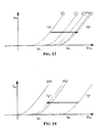
- the trans-characteristics of reference cells in the (VCG, IDS) diagram is shown in Figure 10.
- the RV reference cell is used to discriminate if a memory cell (bit) must be classified as a logical 1 (erased) or a logical 0 (programmed).
- the reading of a bit is effected by comparing drain current (IDS) of the selected cell array cell with that of the RV reference cell by a sense amplifier (briefly "sense").
- IDS drain current
- the two currents are converted in voltage values (mat-side & ref-side) that are sensed by using a differential amplifier.
- the sense amp outputs a logical value 0 or 1 depending on the result of comparison.
- the EV reference cell is used to determine if a cell has been sufficiently erased after an erase pulse applied to the cell (together to the other cells that compose at least a unit of information).
- an erase pulse may cause some of the cells to get over erased and become depleted (Vt ⁇ 0)
- a soft programming operation needs to be performed after a successful erase verify to bring any depleted cell above DV reference cell threshold.
- reference cells are Flash cells formed close to the memory cell array and are contained in a minuscule array. With present fabrication technologies, this permits to achieve a sufficient match in terms of geometrical and electrical characteristics between the flash cells of the memory array and phase of reference cell array. These cells are accessible for programming & read operations singularly, however during erase, they are erased all together. In ultra-violet (UV) condition, all the reference cells have a threshold that is statistically distributed according to a Gaussian law with mean value V RCUV . Target values of threshold for the four reference cells mentioned above are determined through a characterization that is done during the phase of process and cell development.
- UV ultra-violet
- DMA direct measurement
- DMA direct memory access
- a fixed voltage e.g. 1V
- PMU parametrimetric measurement Unit
- the path between the cell drain and the PMU is enabled by activating relative test-mode latches.
- the PMU is a measurement unit that is commonly available in memory testers that is capable of forcing a voltage and measure the current sunk or vice versa.
- the PMU is an expensive hardware resource and can be connected to any of the test channels.
- that channel must be disconnected from the normal pad electronics of the tester (for driving CMOS or TTL logical levels) by using mechanical relays. This intervention, if not performed in the right sequence, may cause the "hot" switching of relays and damage the tester's pin electronics and the device under test itself. Therefore, PMU connect/disconnect sequences require resetting the device pads to a predetermined standard condition (that may be design dependent, normally at 0V) before connecting/disconnecting the PMU.
- the PMU has been connected to a cell, it has to force a predefined fixed voltage (1V) on the cell drain and make sure that the voltage level is stable before carrying out the current measurement. It is evident that a considerable time is taken by these conditioning phases during the verify operation. Usually these wait times are larger than the programming time and these delays when multiplied by the number of reference cells to be checked, became significant.
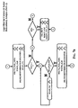
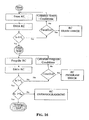
- the flow diagram of Figure 16 illustrates the test flow sequence of reference cell setting.
- the first phase is an erase step followed by a DMA check after each erase pulse whereby the pulse width to be used for the next erase pulse is calculated in function of the "distance" from the target value Ic.
- a predetermined value Erase Timeout
- the second phase as said above is the programming phase of the selected cell, each program pulse being followed by a program verify step that determines the successive pulse in function of the "distance" from the target value Ip until the current measured is less than Ip.
- a check phase consists in checking for eventual over programming, i.e. if the current of any of the cells is less than lop (min allowable current value for that reference) an over programming error is signaled.
- the time necessary to set the reference cells is reduced by almost 90% by avoiding recourse to a DMA technique using external testing implements.
- the setting of the reference cell according to the flow chart of Figure 16 is implemented by exploiting the embedded micro sequencer (MICRO) capable of reading the necessary data either from an embedded ROM or from a cache, e.g. GLOBAL_CACHE.
- MICRO embedded micro sequencer
- the architecture is realized by the following fundamental blocks.
- the architecture includes means to obtain the information regarding the actual cell threshold distance from the predefined target value in a digital form and uses it to adapt the duration of the program pulse and the programming gate voltage for an eventual successive program pulse.
- the architecture provides outstanding flexibility by allowing the downloading of any programming/erase algorithm in the GLOBAL CACHE and does not require the use of external PMU for performing the necessary current measurements.
- the latter are performed, using either an internal or an external reference current, by a distance (difference) calculation circuit.
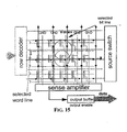
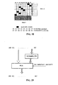
- the target is to have a linear column/row address arrangement. This means that "row0/co10" correspond to row/col address "0", row1/co11 to row/col address "1' and so on, row-n/col-n to address "n".
- fail map is generated on the tester catch memory.
- the analysis of this map is very important to gather information about eventual fabrication process problems.
- These fail maps may evidence a characteristic aspect, said "defect signature", that helps the device engineer to recognize problems and eventually solve them.
- Scrambler memory an external memory, called “Scrambler memory”, present in the tester. This memory links the addresses produced by an internal counter of the tester with the external addresses of the memory to obtain a biunivocal correspondence between successive address values generated by the tester counter and the physical columns of the memory array of the device being tested.
- the content of the scrambler memory is a firmware that is written on specific requests thus an additional constitution cost.
- the firmware changes from a device to another and, for every new device, a new scrambler firmware must be procured.
- the solution is based on the use of a two metal layers matrix (for example realized in Metal1/Metal3) as shown in Figure 18.
- the solution is easy and has a low cost. It only needs single logic circuitry to switch from standard mode to scrambler mode, as shown in Figure 19.
- Vgmin is the maximum supply voltage at which all cells are correctly sensed as a logic "one”
- Vgmax is defined as the minimum voltage at which all cells are correctly sensed as logic "zero”.
- the testing routine defines two voltage ranges in which the two above defined parameters, (vgmin/vgmax), must remain. If this is not satisfied a fail flag will be generated and the part will be rejected.
- pattern All0/All1 is programmed on the whole memory array.
- read operations of the whole matrix are done with a minimum cycle time of about 250ns (almost 2.5 times longer than the typical access time of the slowest flash memory devices) because the testing machine must compare the read data with those written in the same location in a "tester reference memory” to validate each read (pass/fail).
- the in-build architecture of this invention provides an efficient solution.
- the time saved is directly proportional to the size of the memory array under test.
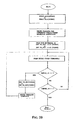
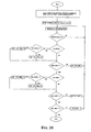
- the flowchart of Figure 20 starts from a programmed/erased device to search vgmax/vgmin values.
- test program through the TUI issues a command sequence to begin embedded vgmax/vgmin search, following with an internal or an external approach.
- the supply voltage is set to 7.5V (for vgmax) or to 1.4V (for vgmin).
- the program commands a read every 500ns, checking values present on DQPAD_15 and DQPAD_14.
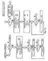
- the flow chart of Figure 21 shows the internal algorithm that is executed by micro to carry out the binary search.
- the flow starts with the loading of the reference current using fdma blocks, and with selecting vgmax or vgmin search in dependence of the sequence command sent to TUI from the test program.
- the starting address location will be set always to 00...00.
- VGMAX a certain voltage value is loaded on the DAC to start the binary search. This value is chosen in the voltage range 7.5V-1.4V.
- the next step is to check the "DATO_OK" flag: if the flag value is equal to '1' the algorithm proceeds to read next location.
- the new value of gate voltage is obtained using DAC circuitry and the counter "COUNTER TENT".
- the algorithm sets the signal "STOP" to '1' and places on DQPAD_15, a '1'.
- a flag FAIL is set on the DQPAD_15 and the execution of the algorithm ends.
- the system of this invention permits to do an automatic search, on a memory flash programmed with a pattern all0/all1, of the gate voltage value at which a logic one or a zero are correctly sensed.
- the architecture of this invention is outstandingly flexible because the voltage supplied to the cells for the read operations may be generated either by an internal DAC or by an external supply.
- An internal DAC is able to change accurately the applied voltage by 125mv steps, while the micro controller can manage a linear search of the pass/fail points during read operation of the memory.
- the programming of these patterns allows an easy detection of shorts between adjacent cells or shorts between selection transistors in the decoding structures.
- data to be programmed on successive locations are generated automatically inside the device as well as the correspondent addresses.
- the system overcomes the burden of writing consecutive user mode program commands for each location and significantly contribute to reduce the testing time.
- the saving of time is directly proportional to the size of the memory array under test.
- the simplicity of the routine greatly helps the test program development and its debugging, while not incrementing the number of gates (silicon area) of the measuring device.
- the system permits automatic programming of any "single-word" starting from whatever word address and whatever data entered as data input, using an embedded algorithm.
- timing is of about 200/300ns cycle time.
- the test starts with a command cycle for embedded programming, sent to the TUI, followed by a write cycle to load the data that the user wants to program in the array (ffff, aaaa, 0000, ff00, etc).
- the algorithm starts on the raising edge of the last write cycle.
- the embedded algorithm will program a CK, a CKN or an ALL0/ALL1 pattern.
- a programming pulse is sent to the addressed memory cells and, at the end of an internal read phase, verifies if the datum is correctly programmed.
- the micro-controller checks whether a ck, ckn pattern, or an all0/all1/diag pattern is requested to be programmed and then waits for the flag value "CK_PROG". It should be remarked the fact that to program a ckn pattern instead of ck, it is sufficient to load the complement of the ck pattern at the last write cycle.
- the value of the "CK_PROG" flag may or may not be set by using two different command sequences depending on the pattern to be programmed whether Ck/Ckn or All0/All1.
- This flag changes its value at each consecutive programming pulse thus realizing a real CK pattern inside the array.
- the algorithm also recognizes if the last column address has arrived and changes twice the value of flag "INV_PGML" to continue the correct sequence of a checkerboard matrix (see FIG.23).
- the system described above permits to do an embedded programming operation of any pattern on the cell matrix, by loading data to be written during the last write cycle.
- This approach reduces testing time during programming operations and the saving may even be enhanced by increasing the word programming parallelism (that is passing to x32 or even to x64 bits).
- Analog node voltage measurement is indispensable to provide device voltage level information.
- the same information and relative test methodology may of course be used for current measurement.
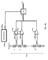
- the in-built analog voltage (or current) measurement system provides digitized information that may be easily gathered by whatever EWS testing machine is used, through normal I/O srtuctures and then processed as a common digital pattern, not requiring any particular analog interface or PMU.
- the reference voltage can be provided internally by a step voltage regulator driven by control signals sent by the micro-controller in execution of a certain algorithm.
- the precision is defined by that or the reference and by the number of the comparators, that is the number intervals in which the voltage range of measurement to cover is divided.
- an in-built voltage measurement structure as described above is faster and does not require a codification.
- the in-built approach of the present inventors permits accurate current and voltage measurements during the testing routine of whatever device while at the same time reducing testing time in terms of measurement time as well of the time for developing-and-debugging of the test software by the testing machine.
Landscapes
- For Increasing The Reliability Of Semiconductor Memories (AREA)
- Read Only Memory (AREA)
Claims (3)
- Dispositif mémoire comprenant un réseau de mémoires flash standard ; un microcontrôleur pour gérer les fonctions des mémoires flash standard, pour un test du dispositif au niveau tranche et en tant que produit fini, pour une analyse de redondance, pour une programmation de mémoires adressables par le contenu (CAM) de reroutage, constitué de deux groupes de cellules flash, et pour la validation du dispositif ; une interface de commande en mode de test (TUI) pour couplage avec un équipement de test externe ; un bloc de circuit (REPAIR-DATA_GEN) incluant un premier registre (REDUNDANCY_REGISTER) dans lequel un vecteur de redondance à programmer dans les CAM de reroutage et des trajets sélectionnés pour les informations de programmation sont mémorisés pendant l'exécution d'un algorithme de programmation de CAM ; le dispositif mémoire comprenant une structure matérielle incorporée pour réaliser des sous-programmes de tests prédéfinis, une analyse de redondance, une programmation des CAM de reroutage et une validation du dispositif de façon interne sans échanger de données avec l'équipement de test externe, comprenant les blocs fonctionnels suivants :une première mémoire cache (LOCAL ADDRESS CACHE) comprenant des seconds registres pour mémoriser jusqu'à un nombre maximum N d'adresses de colonnes dans lesquelles des cellules en défaut sont détectées, égal au nombre de ressources de redondance de colonnes disponibles pour chaque secteur du réseau mémoire standard ;un compteur d'adresse (DEVICE ADDRESS COUNTER) ;un premier circuit (EXPECTED DATA GENERATION) pour produire une donnée attendue quand on lit un certain emplacement mémoire préprogrammé avec la donnée attendue ;un circuit de comparaison (DATA COMPARISON) pour comparer la donnée attendue produite à la donnée lue à partir dudit emplacement mémoire ;un nombre N de troisièmes registres (LOCAL DATA CACHE) égal au nombre de ressources de redondance de colonnes disponibles pour chaque secteur du réseau mémoire standard, chaque registre ayant un nombre M de bits en coïncidence avec le parallélisme lu du réseau mémoire standard, et dans lequel le circuit de comparaison (DATA COMPARISON) lit des informations relatives aux bits sur lesquels un défaut est apparu ;un compteur de module M (BIT POSITION COUNTER) pour analyser bit par bit les N troisièmes registres (LOCAL DATA CACHE) ;un compteur/décompteur (RESOURCE COUNTER) pour pointer vers l'un des registres des N troisièmes registres (LOCAL DATA CACHE), vers l'un des seconds registres de la première mémoire cache (LOCAL ADDRESS CACHE), et vers un emplacement d'une seconde mémoire cache (GLOBAL CACHE) et incluant une bascule pour préserver une valeur de pointeur ;la seconde mémoire cache (GLOBAL CACHE) étant destinée à mémoriser sous forme comprimée des informations relatives à des cellules du réseau en défaut détectées dans un certain secteur auquel on a accédé, en lecture et en écriture, par l'intermédiaire d'un premier bus de données (GLB_CACHE_DATA) et commandé par un second bus (EXT_RD_WR_INTERFACE) provenant de l'interface de commande en mode de test (TUI) et par l'intermédiaire d'un troisième bus (GLB_CACHE-CTRL-BUS) provenant du microcontrôleur (MICRO);un générateur d'adresse de cache (CACHE ADDRESS GENERATOR) pour produire une adresse courante de la seconde mémoire cache (GLOBAL CACHE) à partir d'une adresse courante du compteur d'adresse (DEVICE ADDRESS COUNTER) et du contenu du compteur/décompteur (RESOURCE COUNTER) ;une pluralité de pilotes de bus, commandés par des signaux de commande (WRITE_FAIL_INFO, WRITE_RESOURCE_INFO, WRITE_GLB) gérés par le microcontrôleur (MICRO) pour accéder au premier bus de données (GLB_CACHE_DATA) et de là à la seconde mémoire cache (GLOBAL_CACHE) pour y écrire les informations suivantes :a) le contenu (RESOURCE_INFO) du compteur/décompteur (RESOURCE_COUNTER) ;b) les informations de position des bits en défaut détectés sous forme comprimée (POSITION_INFO) obtenues à partir d'une analyse des N troisièmes registres (LOCAL DATA CACHE) par l'intermédiaire du compteur de module M (BIT POSITION COUNTER) ;c) l'adresse de colonne (ADDRESS_INFO) des colonnes ayant des cellules en défaut détectées ;d) les informations écrites dans la seconde mémoire cache (GLOBAL_CACHE) par l'intermédiaire de l'interface de commande en mode de test (TUI) pour exécuter des routines de tests spécifiques.
- Dispositif mémoire selon la revendication 1, dans lequel l'adresse (SECTOR_ADD) présentement dans le compteur d'adresse (DEVICE ADDRESS COUNTER) est fournie à un premier générateur de pointeur (SECTOR POINTER GENERATOR) et le contenu (RESOURCE_ADD) du compteur/décompteur (RESOURCE COUNTER) est fourni à un second générateur de pointeur (RESOURCE OFFSET GENERATOR), et les données fournies par les premier et second générateurs de pointeur sont combinées par un additionneur binaire couplé à une première entrée (A) d'un multiplexeur (MUX), vers une seconde entrée (B) dont une adresse d'emplacement de mémoire cache est applicable à partir de l'extérieur par l'intermédiaire de l'interface de commande en mode test (TUI) pour la sélection du mode d'accès piloté par un signal de commande externe (USE_EXT_ADDRESS/USE_MSEQ_ADDRESS) par l'interface (TUI).
- Dispositif mémoire selon la revendication 2, dans lequel la seconde mémoire cache (GLOBAL_CACHE) peut être adressée par l'intermédiaire d'un compteur de programme (PROGRAM_COUNTER) utilisé pour adresser une mémoire morte du microcontrôleur, une donnée de pointeur (MICRO ADDRESS) étant fournie à une troisième entrée (C) du multiplexeur (MUX).
Priority Applications (3)
| Application Number | Priority Date | Filing Date | Title |
|---|---|---|---|
| EP03425126A EP1453062B1 (fr) | 2003-02-27 | 2003-02-27 | Méthode de test intégré dans une mémoire Flash |
| DE60306488T DE60306488D1 (de) | 2003-02-27 | 2003-02-27 | Eingebautes Testverfahren in einem Flash Speicher |
| US10/789,443 US7050343B2 (en) | 2003-02-27 | 2004-02-27 | Built-in testing methodology in flash memory |
Applications Claiming Priority (1)
| Application Number | Priority Date | Filing Date | Title |
|---|---|---|---|
| EP03425126A EP1453062B1 (fr) | 2003-02-27 | 2003-02-27 | Méthode de test intégré dans une mémoire Flash |
Publications (2)
| Publication Number | Publication Date |
|---|---|
| EP1453062A1 EP1453062A1 (fr) | 2004-09-01 |
| EP1453062B1 true EP1453062B1 (fr) | 2006-06-28 |
Family
ID=32749052
Family Applications (1)
| Application Number | Title | Priority Date | Filing Date |
|---|---|---|---|
| EP03425126A Expired - Lifetime EP1453062B1 (fr) | 2003-02-27 | 2003-02-27 | Méthode de test intégré dans une mémoire Flash |
Country Status (3)
| Country | Link |
|---|---|
| US (1) | US7050343B2 (fr) |
| EP (1) | EP1453062B1 (fr) |
| DE (1) | DE60306488D1 (fr) |
Cited By (1)
| Publication number | Priority date | Publication date | Assignee | Title |
|---|---|---|---|---|
| US8572361B2 (en) | 2005-07-28 | 2013-10-29 | Micron Technology, Inc. | Configuration of a multilevel flash memory device |
Families Citing this family (39)
| Publication number | Priority date | Publication date | Assignee | Title |
|---|---|---|---|---|
| US8770050B2 (en) * | 2006-03-17 | 2014-07-08 | Jason Vaughn Clark | Method of measuring micro- and nano-scale properties |
| US7206230B2 (en) * | 2005-04-01 | 2007-04-17 | Sandisk Corporation | Use of data latches in cache operations of non-volatile memories |
| US7433247B2 (en) * | 2005-09-26 | 2008-10-07 | Macronix International Co., Ltd. | Method and circuit for reading fuse cells in a nonvolatile memory during power-up |
| EP1881505A1 (fr) * | 2006-07-20 | 2008-01-23 | STMicroelectronics S.r.l. | Mémoire avec microprocesseur intégré pour la détection et la réparation autonome d'erreurs |
| US7356442B1 (en) * | 2006-10-05 | 2008-04-08 | International Business Machines Corporation | End of life prediction of flash memory |
| US7549098B2 (en) * | 2006-12-19 | 2009-06-16 | International Business Machines Corporation | Redundancy programming for a memory device |
| US7954028B2 (en) * | 2006-12-19 | 2011-05-31 | International Business Machines Corporation | Structure for redundancy programming of a memory device |
| KR100855974B1 (ko) * | 2007-01-26 | 2008-09-02 | 삼성전자주식회사 | 웨이퍼 테스트용 패드를 구비하는 반도체 집적 회로 및반도체 집적 회로를 포함하는 웨이퍼의 테스트 방법 |
| US7512509B2 (en) | 2007-04-26 | 2009-03-31 | International Business Machines Corporation | M1 testable addressable array for device parameter characterization |
| US8131387B2 (en) * | 2007-08-09 | 2012-03-06 | Teradyne, Inc. | Integrated high-efficiency microwave sourcing control process |
| US8125835B2 (en) | 2008-09-22 | 2012-02-28 | Cypress Semiconductor Corporation | Memory architecture having two independently controlled voltage pumps |
| JP2011134410A (ja) * | 2009-12-25 | 2011-07-07 | Toshiba Corp | 不揮発性半導体記憶装置及びその試験方法 |
| US8320185B2 (en) * | 2010-03-31 | 2012-11-27 | Micron Technology, Inc. | Lifetime markers for memory devices |
| WO2013048500A1 (fr) | 2011-09-30 | 2013-04-04 | Intel Corporation | Appareil et procédé pour mettre en œuvre une hiérarchie de mémoire multiniveau sur des canaux de mémoire communs |
| US9378142B2 (en) * | 2011-09-30 | 2016-06-28 | Intel Corporation | Apparatus and method for implementing a multi-level memory hierarchy having different operating modes |
| EP2761466B1 (fr) | 2011-09-30 | 2020-08-05 | Intel Corporation | Appareil et procédé pour mette en uvre une hiérarchie de mémoire multiniveau |
| EP3364304B1 (fr) | 2011-09-30 | 2022-06-15 | INTEL Corporation | Canal de mémoire prenant en charge l'accès à la mémoire proche et lointaine |
| TWI453586B (zh) * | 2011-12-02 | 2014-09-21 | Giga Byte Tech Co Ltd | 顯示卡及其資訊儲存方法 |
| ITMI20120595A1 (it) * | 2012-04-12 | 2013-10-13 | St Microelectronics Srl | Gestione della cancellazione di pagine operative di un dispositivo di memoria flash tramite pagine di servizio |
| US8996934B2 (en) | 2012-09-29 | 2015-03-31 | Intel Corporation | Transaction-level testing of memory I/O and memory device |
| US9003246B2 (en) | 2012-09-29 | 2015-04-07 | Intel Corporation | Functional memory array testing with a transaction-level test engine |
| US8886991B2 (en) * | 2012-10-26 | 2014-11-11 | Lsi Corporation | Sector failure prediction method and related system |
| US9009540B2 (en) | 2012-12-05 | 2015-04-14 | Intel Corporation | Memory subsystem command bus stress testing |
| US9009531B2 (en) * | 2012-12-05 | 2015-04-14 | Intel Corporation | Memory subsystem data bus stress testing |
| US9477548B2 (en) * | 2014-08-01 | 2016-10-25 | Freescale Semiconductor, Inc. | Error repair location cache |
| TWI563581B (en) * | 2015-01-26 | 2016-12-21 | Winbond Electronics Corp | Flash memory wafer probing method and machine |
| US9830998B2 (en) | 2015-05-19 | 2017-11-28 | Sandisk Technologies Llc | Stress patterns to detect shorts in three dimensional non-volatile memory |
| TWI566251B (zh) * | 2015-06-25 | 2017-01-11 | 華邦電子股份有限公司 | 快閃記憶體晶圓測試方法以及機台 |
| CN105206305B (zh) * | 2015-09-22 | 2018-08-21 | 上海华虹宏力半导体制造有限公司 | 通过测试程序增加flash器件窗口的方法 |
| US10559374B2 (en) | 2017-02-20 | 2020-02-11 | Piecemakers Technology, Inc. | Circuit topology of memory chips with embedded function test pattern generation module connected to normal access port physical layer |
| US10387239B2 (en) * | 2017-04-10 | 2019-08-20 | Western Digital Technologies, Inc. | Detecting memory failures in the runtime environment |
| US10467439B2 (en) * | 2017-07-05 | 2019-11-05 | Dell Products, L.P. | Detecting tampering of memory contents in an information handling system |
| US10347317B2 (en) * | 2017-10-05 | 2019-07-09 | Gyrfalcon Technology Inc. | Method of self-testing and reusing of reference cells in a memory architecture |
| US11146289B2 (en) | 2019-03-29 | 2021-10-12 | Intel Corporation | Techniques to use intrinsic information for a bit-flipping error correction control decoder |
| CN111949426B (zh) * | 2019-05-16 | 2024-09-17 | 兆易创新科技集团股份有限公司 | 一种固件程序错误的检测方法、装置及存储设备 |
| US11063607B2 (en) * | 2019-05-24 | 2021-07-13 | Intel Corporation | Compressing error vectors for decoding logic to store compressed in a decoder memory used by the decoding logic |
| US11868693B2 (en) * | 2021-04-21 | 2024-01-09 | Siemens Industry Software Inc. | Verification performance profiling with selective data reduction |
| TWI845062B (zh) * | 2022-12-13 | 2024-06-11 | 慧榮科技股份有限公司 | 對快閃記憶體模組進行測試的方法、與相關的快閃記憶體控制器及記憶裝置 |
| TWI882772B (zh) * | 2024-04-18 | 2025-05-01 | 華邦電子股份有限公司 | 記憶體裝置及其控制方法 |
Family Cites Families (8)
| Publication number | Priority date | Publication date | Assignee | Title |
|---|---|---|---|---|
| GB1158010A (en) * | 1966-12-21 | 1969-07-09 | Ibm | Data Storage Apparatus |
| FR2655177A1 (fr) * | 1989-11-24 | 1991-05-31 | Sgs Thomson Microelectronics | Circuit de redondance avec memorisation de position de plot de sortie. |
| US5732207A (en) * | 1995-02-28 | 1998-03-24 | Intel Corporation | Microprocessor having single poly-silicon EPROM memory for programmably controlling optional features |
| US5633877A (en) * | 1995-05-31 | 1997-05-27 | International Business Machines Corporation | Programmable built-in self test method and controller for arrays |
| US6253289B1 (en) * | 1998-05-29 | 2001-06-26 | Compaq Computer Corporation | Maximizing sequential read streams while minimizing the impact on cache and other applications |
| EP1206775B1 (fr) * | 1999-08-23 | 2004-11-10 | Micron Technology, Inc. | Detection et reparation des fuites declenchees exterieurement |
| JP4165990B2 (ja) * | 1999-12-20 | 2008-10-15 | Tdk株式会社 | メモリコントローラ及びメモリコントローラを備えるフラッシュメモリシステム、並びに、フラッシュメモリへのデータの書き込み方法 |
| JP4191355B2 (ja) * | 2000-02-10 | 2008-12-03 | 株式会社ルネサステクノロジ | 半導体集積回路装置 |
-
2003
- 2003-02-27 EP EP03425126A patent/EP1453062B1/fr not_active Expired - Lifetime
- 2003-02-27 DE DE60306488T patent/DE60306488D1/de not_active Expired - Lifetime
-
2004
- 2004-02-27 US US10/789,443 patent/US7050343B2/en not_active Expired - Fee Related
Cited By (1)
| Publication number | Priority date | Publication date | Assignee | Title |
|---|---|---|---|---|
| US8572361B2 (en) | 2005-07-28 | 2013-10-29 | Micron Technology, Inc. | Configuration of a multilevel flash memory device |
Also Published As
| Publication number | Publication date |
|---|---|
| EP1453062A1 (fr) | 2004-09-01 |
| US20040218440A1 (en) | 2004-11-04 |
| DE60306488D1 (de) | 2006-08-10 |
| US7050343B2 (en) | 2006-05-23 |
Similar Documents
| Publication | Publication Date | Title |
|---|---|---|
| US7050343B2 (en) | Built-in testing methodology in flash memory | |
| US7284167B2 (en) | Automated tests for built-in self test | |
| KR100328615B1 (ko) | 메모리 시험장치 | |
| US6396742B1 (en) | Testing of multilevel semiconductor memory | |
| USRE37611E1 (en) | Non-volatile memory system having internal data verification test mode | |
| JP4790110B2 (ja) | 回路内メモリ・アレイ・ビット・セル・スレシホルド電圧分布測定 | |
| US7062689B2 (en) | Method and apparatus for memory self testing | |
| US7646655B2 (en) | Memory device with fail search and redundancy | |
| US8201037B2 (en) | Semiconductor integrated circuit and method for controlling semiconductor integrated circuit | |
| US20040123181A1 (en) | Self-repair of memory arrays using preallocated redundancy (PAR) architecture | |
| US20030037295A1 (en) | Non-volatile memory device with self test | |
| WO1994024674A1 (fr) | Testeur de memoire a semiconducteurs | |
| CN101611456A (zh) | 具有用于测试快闪存储器的串行接口的嵌入式架构 | |
| CN103187102B (zh) | 半导体存储器测试方法和半导体存储器 | |
| JP2006162285A (ja) | 半導体集積回路のテスト装置および方法 | |
| US11495313B1 (en) | Fail-safe IC production testing | |
| US7672803B1 (en) | Input of test conditions and output generation for built-in self test | |
| CN120564810A (zh) | Dram的修复方法、上位机、存储介质及计算机程序产品 | |
| US7415646B1 (en) | Page—EXE erase algorithm for flash memory | |
| US20070036007A1 (en) | Sticky bit buffer | |
| US7518918B2 (en) | Method and apparatus for repairing embedded memory in an integrated circuit | |
| US20220139493A1 (en) | Memory device and operating method thereof | |
| JPH0823016A (ja) | 半導体メモリのテスト方法 | |
| CN114649049B (zh) | Cam单元检查模块及其检查方法 | |
| US7929363B1 (en) | Memory test and setup method |
Legal Events
| Date | Code | Title | Description |
|---|---|---|---|
| PUAI | Public reference made under article 153(3) epc to a published international application that has entered the european phase |
Free format text: ORIGINAL CODE: 0009012 |
|
| AK | Designated contracting states |
Kind code of ref document: A1 Designated state(s): AT BE BG CH CY CZ DE DK EE ES FI FR GB GR HU IE IT LI LU MC NL PT SE SI SK TR |
|
| AX | Request for extension of the european patent |
Extension state: AL LT LV MK RO |
|
| 17P | Request for examination filed |
Effective date: 20050205 |
|
| AKX | Designation fees paid |
Designated state(s): DE FR GB IT |
|
| GRAP | Despatch of communication of intention to grant a patent |
Free format text: ORIGINAL CODE: EPIDOSNIGR1 |
|
| RIN1 | Information on inventor provided before grant (corrected) |
Inventor name: TOMAIUOLO, FRANCESCO Inventor name: KUMAR, PROMOD Inventor name: NICOSIA, PIERPAOLO Inventor name: DE AMBROGGI, LUCA GIUSEPPE Inventor name: PIPITONE, FRANCESCO |
|
| GRAS | Grant fee paid |
Free format text: ORIGINAL CODE: EPIDOSNIGR3 |
|
| GRAA | (expected) grant |
Free format text: ORIGINAL CODE: 0009210 |
|
| AK | Designated contracting states |
Kind code of ref document: B1 Designated state(s): DE FR GB IT |
|
| PG25 | Lapsed in a contracting state [announced via postgrant information from national office to epo] |
Ref country code: IT Free format text: LAPSE BECAUSE OF FAILURE TO SUBMIT A TRANSLATION OF THE DESCRIPTION OR TO PAY THE FEE WITHIN THE PRESCRIBED TIME-LIMIT;WARNING: LAPSES OF ITALIAN PATENTS WITH EFFECTIVE DATE BEFORE 2007 MAY HAVE OCCURRED AT ANY TIME BEFORE 2007. THE CORRECT EFFECTIVE DATE MAY BE DIFFERENT FROM THE ONE RECORDED. Effective date: 20060628 |
|
| REG | Reference to a national code |
Ref country code: GB Ref legal event code: FG4D |
|
| REF | Corresponds to: |
Ref document number: 60306488 Country of ref document: DE Date of ref document: 20060810 Kind code of ref document: P |
|
| PG25 | Lapsed in a contracting state [announced via postgrant information from national office to epo] |
Ref country code: DE Free format text: LAPSE BECAUSE OF FAILURE TO SUBMIT A TRANSLATION OF THE DESCRIPTION OR TO PAY THE FEE WITHIN THE PRESCRIBED TIME-LIMIT Effective date: 20060929 |
|
| ET | Fr: translation filed | ||
| PLBE | No opposition filed within time limit |
Free format text: ORIGINAL CODE: 0009261 |
|
| STAA | Information on the status of an ep patent application or granted ep patent |
Free format text: STATUS: NO OPPOSITION FILED WITHIN TIME LIMIT |
|
| 26N | No opposition filed |
Effective date: 20070329 |
|
| PGFP | Annual fee paid to national office [announced via postgrant information from national office to epo] |
Ref country code: IT Payment date: 20080212 Year of fee payment: 6 |
|
| PGFP | Annual fee paid to national office [announced via postgrant information from national office to epo] |
Ref country code: GB Payment date: 20090128 Year of fee payment: 7 |
|
| PGFP | Annual fee paid to national office [announced via postgrant information from national office to epo] |
Ref country code: FR Payment date: 20090226 Year of fee payment: 7 |
|
| GBPC | Gb: european patent ceased through non-payment of renewal fee |
Effective date: 20100227 |
|
| REG | Reference to a national code |
Ref country code: FR Ref legal event code: ST Effective date: 20101029 |
|
| PG25 | Lapsed in a contracting state [announced via postgrant information from national office to epo] |
Ref country code: FR Free format text: LAPSE BECAUSE OF NON-PAYMENT OF DUE FEES Effective date: 20100301 |
|
| PG25 | Lapsed in a contracting state [announced via postgrant information from national office to epo] |
Ref country code: GB Free format text: LAPSE BECAUSE OF NON-PAYMENT OF DUE FEES Effective date: 20100227 Ref country code: IT Free format text: LAPSE BECAUSE OF NON-PAYMENT OF DUE FEES Effective date: 20090227 |