EP1453112B1 - Lichtemittierende Vorrichtung und dessen Herstellungsverfahren - Google Patents
Lichtemittierende Vorrichtung und dessen Herstellungsverfahren Download PDFInfo
- Publication number
- EP1453112B1 EP1453112B1 EP04011150.2A EP04011150A EP1453112B1 EP 1453112 B1 EP1453112 B1 EP 1453112B1 EP 04011150 A EP04011150 A EP 04011150A EP 1453112 B1 EP1453112 B1 EP 1453112B1
- Authority
- EP
- European Patent Office
- Prior art keywords
- layer
- active layer
- light emitting
- type
- forming
- Prior art date
- Legal status (The legal status is an assumption and is not a legal conclusion. Google has not performed a legal analysis and makes no representation as to the accuracy of the status listed.)
- Expired - Lifetime
Links
- 238000004519 manufacturing process Methods 0.000 title claims description 25
- 238000005253 cladding Methods 0.000 claims description 75
- 229910002704 AlGaN Inorganic materials 0.000 claims description 60
- 239000004065 semiconductor Substances 0.000 claims description 56
- 150000004767 nitrides Chemical class 0.000 claims description 27
- 229910052738 indium Inorganic materials 0.000 claims description 17
- APFVFJFRJDLVQX-UHFFFAOYSA-N indium atom Chemical compound [In] APFVFJFRJDLVQX-UHFFFAOYSA-N 0.000 claims description 17
- 238000000034 method Methods 0.000 claims description 16
- 239000012535 impurity Substances 0.000 claims description 13
- 150000001875 compounds Chemical class 0.000 claims description 10
- 239000013078 crystal Substances 0.000 description 34
- 239000000758 substrate Substances 0.000 description 23
- XCZXGTMEAKBVPV-UHFFFAOYSA-N trimethylgallium Chemical compound C[Ga](C)C XCZXGTMEAKBVPV-UHFFFAOYSA-N 0.000 description 22
- 230000008030 elimination Effects 0.000 description 17
- 238000003379 elimination reaction Methods 0.000 description 17
- QGZKDVFQNNGYKY-UHFFFAOYSA-N Ammonia Chemical compound N QGZKDVFQNNGYKY-UHFFFAOYSA-N 0.000 description 16
- 239000000470 constituent Substances 0.000 description 15
- 239000007789 gas Substances 0.000 description 12
- 230000015572 biosynthetic process Effects 0.000 description 11
- 238000009792 diffusion process Methods 0.000 description 11
- 238000001947 vapour-phase growth Methods 0.000 description 10
- 229910021529 ammonia Inorganic materials 0.000 description 8
- 230000004888 barrier function Effects 0.000 description 8
- 239000012159 carrier gas Substances 0.000 description 8
- 238000010586 diagram Methods 0.000 description 8
- 239000000463 material Substances 0.000 description 8
- 230000000903 blocking effect Effects 0.000 description 7
- 238000005229 chemical vapour deposition Methods 0.000 description 6
- 230000006866 deterioration Effects 0.000 description 6
- 239000002019 doping agent Substances 0.000 description 6
- 230000000694 effects Effects 0.000 description 6
- JLTRXTDYQLMHGR-UHFFFAOYSA-N trimethylaluminium Chemical compound C[Al](C)C JLTRXTDYQLMHGR-UHFFFAOYSA-N 0.000 description 6
- 229910052594 sapphire Inorganic materials 0.000 description 5
- 239000010980 sapphire Substances 0.000 description 5
- 230000007547 defect Effects 0.000 description 4
- 229910016920 AlzGa1−z Inorganic materials 0.000 description 3
- 229910052751 metal Inorganic materials 0.000 description 3
- 239000002184 metal Substances 0.000 description 3
- IJGRMHOSHXDMSA-UHFFFAOYSA-N Atomic nitrogen Chemical compound N#N IJGRMHOSHXDMSA-UHFFFAOYSA-N 0.000 description 2
- MHYQBXJRURFKIN-UHFFFAOYSA-N C1(C=CC=C1)[Mg] Chemical compound C1(C=CC=C1)[Mg] MHYQBXJRURFKIN-UHFFFAOYSA-N 0.000 description 2
- BLRPTPMANUNPDV-UHFFFAOYSA-N Silane Chemical compound [SiH4] BLRPTPMANUNPDV-UHFFFAOYSA-N 0.000 description 2
- VYPSYNLAJGMNEJ-UHFFFAOYSA-N Silicium dioxide Chemical compound O=[Si]=O VYPSYNLAJGMNEJ-UHFFFAOYSA-N 0.000 description 2
- 238000004891 communication Methods 0.000 description 2
- HQWPLXHWEZZGKY-UHFFFAOYSA-N diethylzinc Chemical compound CC[Zn]CC HQWPLXHWEZZGKY-UHFFFAOYSA-N 0.000 description 2
- 238000005530 etching Methods 0.000 description 2
- 230000008020 evaporation Effects 0.000 description 2
- 238000001704 evaporation Methods 0.000 description 2
- 238000010438 heat treatment Methods 0.000 description 2
- 239000004973 liquid crystal related substance Substances 0.000 description 2
- 230000003287 optical effect Effects 0.000 description 2
- RGGPNXQUMRMPRA-UHFFFAOYSA-N triethylgallium Chemical compound CC[Ga](CC)CC RGGPNXQUMRMPRA-UHFFFAOYSA-N 0.000 description 2
- IBEFSUTVZWZJEL-UHFFFAOYSA-N trimethylindium Chemical compound C[In](C)C IBEFSUTVZWZJEL-UHFFFAOYSA-N 0.000 description 2
- 238000002441 X-ray diffraction Methods 0.000 description 1
- 229910052681 coesite Inorganic materials 0.000 description 1
- 238000005336 cracking Methods 0.000 description 1
- 229910052906 cristobalite Inorganic materials 0.000 description 1
- 238000001093 holography Methods 0.000 description 1
- 230000006872 improvement Effects 0.000 description 1
- 239000012212 insulator Substances 0.000 description 1
- 238000010884 ion-beam technique Methods 0.000 description 1
- 238000005259 measurement Methods 0.000 description 1
- 229910052757 nitrogen Inorganic materials 0.000 description 1
- 239000013307 optical fiber Substances 0.000 description 1
- 230000009467 reduction Effects 0.000 description 1
- 239000000377 silicon dioxide Substances 0.000 description 1
- 238000009751 slip forming Methods 0.000 description 1
- 238000001228 spectrum Methods 0.000 description 1
- 229910052682 stishovite Inorganic materials 0.000 description 1
- 230000007704 transition Effects 0.000 description 1
- 229910052905 tridymite Inorganic materials 0.000 description 1
Images


Classifications
-
- H—ELECTRICITY
- H01—ELECTRIC ELEMENTS
- H01S—DEVICES USING THE PROCESS OF LIGHT AMPLIFICATION BY STIMULATED EMISSION OF RADIATION [LASER] TO AMPLIFY OR GENERATE LIGHT; DEVICES USING STIMULATED EMISSION OF ELECTROMAGNETIC RADIATION IN WAVE RANGES OTHER THAN OPTICAL
- H01S5/00—Semiconductor lasers
- H01S5/30—Structure or shape of the active region; Materials used for the active region
- H01S5/32—Structure or shape of the active region; Materials used for the active region comprising PN junctions, e.g. hetero- or double- heterostructures
- H01S5/321—Structure or shape of the active region; Materials used for the active region comprising PN junctions, e.g. hetero- or double- heterostructures having intermediate bandgap layers
-
- H—ELECTRICITY
- H10—SEMICONDUCTOR DEVICES; ELECTRIC SOLID-STATE DEVICES NOT OTHERWISE PROVIDED FOR
- H10H—INORGANIC LIGHT-EMITTING SEMICONDUCTOR DEVICES HAVING POTENTIAL BARRIERS
- H10H20/00—Individual inorganic light-emitting semiconductor devices having potential barriers, e.g. light-emitting diodes [LED]
- H10H20/80—Constructional details
- H10H20/81—Bodies
- H10H20/822—Materials of the light-emitting regions
- H10H20/824—Materials of the light-emitting regions comprising only Group III-V materials, e.g. GaP
- H10H20/825—Materials of the light-emitting regions comprising only Group III-V materials, e.g. GaP containing nitrogen, e.g. GaN
-
- H—ELECTRICITY
- H01—ELECTRIC ELEMENTS
- H01S—DEVICES USING THE PROCESS OF LIGHT AMPLIFICATION BY STIMULATED EMISSION OF RADIATION [LASER] TO AMPLIFY OR GENERATE LIGHT; DEVICES USING STIMULATED EMISSION OF ELECTROMAGNETIC RADIATION IN WAVE RANGES OTHER THAN OPTICAL
- H01S5/00—Semiconductor lasers
- H01S5/20—Structure or shape of the semiconductor body to guide the optical wave ; Confining structures perpendicular to the optical axis, e.g. index or gain guiding, stripe geometry, broad area lasers, gain tailoring, transverse or lateral reflectors, special cladding structures, MQW barrier reflection layers
- H01S5/22—Structure or shape of the semiconductor body to guide the optical wave ; Confining structures perpendicular to the optical axis, e.g. index or gain guiding, stripe geometry, broad area lasers, gain tailoring, transverse or lateral reflectors, special cladding structures, MQW barrier reflection layers having a ridge or stripe structure
- H01S5/2202—Structure or shape of the semiconductor body to guide the optical wave ; Confining structures perpendicular to the optical axis, e.g. index or gain guiding, stripe geometry, broad area lasers, gain tailoring, transverse or lateral reflectors, special cladding structures, MQW barrier reflection layers having a ridge or stripe structure by making a groove in the upper laser structure
-
- H—ELECTRICITY
- H10—SEMICONDUCTOR DEVICES; ELECTRIC SOLID-STATE DEVICES NOT OTHERWISE PROVIDED FOR
- H10H—INORGANIC LIGHT-EMITTING SEMICONDUCTOR DEVICES HAVING POTENTIAL BARRIERS
- H10H20/00—Individual inorganic light-emitting semiconductor devices having potential barriers, e.g. light-emitting diodes [LED]
- H10H20/01—Manufacture or treatment
- H10H20/011—Manufacture or treatment of bodies, e.g. forming semiconductor layers
- H10H20/013—Manufacture or treatment of bodies, e.g. forming semiconductor layers having light-emitting regions comprising only Group III-V materials
- H10H20/0133—Manufacture or treatment of bodies, e.g. forming semiconductor layers having light-emitting regions comprising only Group III-V materials with a substrate not being Group III-V materials
- H10H20/01335—Manufacture or treatment of bodies, e.g. forming semiconductor layers having light-emitting regions comprising only Group III-V materials with a substrate not being Group III-V materials the light-emitting regions comprising nitride materials
-
- H—ELECTRICITY
- H10—SEMICONDUCTOR DEVICES; ELECTRIC SOLID-STATE DEVICES NOT OTHERWISE PROVIDED FOR
- H10H—INORGANIC LIGHT-EMITTING SEMICONDUCTOR DEVICES HAVING POTENTIAL BARRIERS
- H10H20/00—Individual inorganic light-emitting semiconductor devices having potential barriers, e.g. light-emitting diodes [LED]
- H10H20/80—Constructional details
- H10H20/81—Bodies
-
- H—ELECTRICITY
- H01—ELECTRIC ELEMENTS
- H01S—DEVICES USING THE PROCESS OF LIGHT AMPLIFICATION BY STIMULATED EMISSION OF RADIATION [LASER] TO AMPLIFY OR GENERATE LIGHT; DEVICES USING STIMULATED EMISSION OF ELECTROMAGNETIC RADIATION IN WAVE RANGES OTHER THAN OPTICAL
- H01S2301/00—Functional characteristics
- H01S2301/17—Semiconductor lasers comprising special layers
- H01S2301/173—The laser chip comprising special buffer layers, e.g. dislocation prevention or reduction
-
- H—ELECTRICITY
- H01—ELECTRIC ELEMENTS
- H01S—DEVICES USING THE PROCESS OF LIGHT AMPLIFICATION BY STIMULATED EMISSION OF RADIATION [LASER] TO AMPLIFY OR GENERATE LIGHT; DEVICES USING STIMULATED EMISSION OF ELECTROMAGNETIC RADIATION IN WAVE RANGES OTHER THAN OPTICAL
- H01S2304/00—Special growth methods for semiconductor lasers
- H01S2304/04—MOCVD or MOVPE
-
- H—ELECTRICITY
- H01—ELECTRIC ELEMENTS
- H01S—DEVICES USING THE PROCESS OF LIGHT AMPLIFICATION BY STIMULATED EMISSION OF RADIATION [LASER] TO AMPLIFY OR GENERATE LIGHT; DEVICES USING STIMULATED EMISSION OF ELECTROMAGNETIC RADIATION IN WAVE RANGES OTHER THAN OPTICAL
- H01S5/00—Semiconductor lasers
- H01S5/02—Structural details or components not essential to laser action
- H01S5/0206—Substrates, e.g. growth, shape, material, removal or bonding
- H01S5/0213—Sapphire, quartz or diamond based substrates
-
- H—ELECTRICITY
- H01—ELECTRIC ELEMENTS
- H01S—DEVICES USING THE PROCESS OF LIGHT AMPLIFICATION BY STIMULATED EMISSION OF RADIATION [LASER] TO AMPLIFY OR GENERATE LIGHT; DEVICES USING STIMULATED EMISSION OF ELECTROMAGNETIC RADIATION IN WAVE RANGES OTHER THAN OPTICAL
- H01S5/00—Semiconductor lasers
- H01S5/20—Structure or shape of the semiconductor body to guide the optical wave ; Confining structures perpendicular to the optical axis, e.g. index or gain guiding, stripe geometry, broad area lasers, gain tailoring, transverse or lateral reflectors, special cladding structures, MQW barrier reflection layers
- H01S5/22—Structure or shape of the semiconductor body to guide the optical wave ; Confining structures perpendicular to the optical axis, e.g. index or gain guiding, stripe geometry, broad area lasers, gain tailoring, transverse or lateral reflectors, special cladding structures, MQW barrier reflection layers having a ridge or stripe structure
- H01S5/2205—Structure or shape of the semiconductor body to guide the optical wave ; Confining structures perpendicular to the optical axis, e.g. index or gain guiding, stripe geometry, broad area lasers, gain tailoring, transverse or lateral reflectors, special cladding structures, MQW barrier reflection layers having a ridge or stripe structure comprising special burying or current confinement layers
- H01S5/2206—Structure or shape of the semiconductor body to guide the optical wave ; Confining structures perpendicular to the optical axis, e.g. index or gain guiding, stripe geometry, broad area lasers, gain tailoring, transverse or lateral reflectors, special cladding structures, MQW barrier reflection layers having a ridge or stripe structure comprising special burying or current confinement layers based on III-V materials
- H01S5/221—Structure or shape of the semiconductor body to guide the optical wave ; Confining structures perpendicular to the optical axis, e.g. index or gain guiding, stripe geometry, broad area lasers, gain tailoring, transverse or lateral reflectors, special cladding structures, MQW barrier reflection layers having a ridge or stripe structure comprising special burying or current confinement layers based on III-V materials containing aluminium
-
- H—ELECTRICITY
- H01—ELECTRIC ELEMENTS
- H01S—DEVICES USING THE PROCESS OF LIGHT AMPLIFICATION BY STIMULATED EMISSION OF RADIATION [LASER] TO AMPLIFY OR GENERATE LIGHT; DEVICES USING STIMULATED EMISSION OF ELECTROMAGNETIC RADIATION IN WAVE RANGES OTHER THAN OPTICAL
- H01S5/00—Semiconductor lasers
- H01S5/20—Structure or shape of the semiconductor body to guide the optical wave ; Confining structures perpendicular to the optical axis, e.g. index or gain guiding, stripe geometry, broad area lasers, gain tailoring, transverse or lateral reflectors, special cladding structures, MQW barrier reflection layers
- H01S5/22—Structure or shape of the semiconductor body to guide the optical wave ; Confining structures perpendicular to the optical axis, e.g. index or gain guiding, stripe geometry, broad area lasers, gain tailoring, transverse or lateral reflectors, special cladding structures, MQW barrier reflection layers having a ridge or stripe structure
- H01S5/223—Buried stripe structure
- H01S5/2231—Buried stripe structure with inner confining structure only between the active layer and the upper electrode
-
- H—ELECTRICITY
- H01—ELECTRIC ELEMENTS
- H01S—DEVICES USING THE PROCESS OF LIGHT AMPLIFICATION BY STIMULATED EMISSION OF RADIATION [LASER] TO AMPLIFY OR GENERATE LIGHT; DEVICES USING STIMULATED EMISSION OF ELECTROMAGNETIC RADIATION IN WAVE RANGES OTHER THAN OPTICAL
- H01S5/00—Semiconductor lasers
- H01S5/30—Structure or shape of the active region; Materials used for the active region
- H01S5/32—Structure or shape of the active region; Materials used for the active region comprising PN junctions, e.g. hetero- or double- heterostructures
- H01S5/323—Structure or shape of the active region; Materials used for the active region comprising PN junctions, e.g. hetero- or double- heterostructures in AIIIBV compounds, e.g. AlGaAs-laser, InP-based laser
- H01S5/32308—Structure or shape of the active region; Materials used for the active region comprising PN junctions, e.g. hetero- or double- heterostructures in AIIIBV compounds, e.g. AlGaAs-laser, InP-based laser emitting light at a wavelength less than 900 nm
- H01S5/32341—Structure or shape of the active region; Materials used for the active region comprising PN junctions, e.g. hetero- or double- heterostructures in AIIIBV compounds, e.g. AlGaAs-laser, InP-based laser emitting light at a wavelength less than 900 nm blue laser based on GaN or GaP
Definitions
- the present invention relates to a light emitting device and a manufacturing method thereof.
- Light emitting devices such as light emitting diodes and semiconductor laser devices which are formed of III-V group nitride system semiconductors such as GaN, AlGaN, InGaN and InAlGaN are receiving a great deal of attention because they are capable of, by direct transition, light emission in the yellow to ultraviolet region, especially in the blue region, with large luminous intensity.
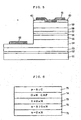
- Fig.8 is a schematic cross-sectional view shoving a conventional light emitting diode composed of III-V group nitride system semiconductors.
- a GaN buffer layer 102 formed in order on a sapphire substrate 101 are a GaN buffer layer 102, an n-type GaN contact layer 103 also serving as an n-type cladding layer, an InGaN active layer 104, a p-type AlGaN cladding layer 105, and a p-type GaN contact layer 106 .
- a p electrode 107 is formed on the p-type GaN contact layer 106 and an n electrode 108 is formed on the n-type GaN contact layer 103.
- This light emitting diode is grown by metal organic chemical vapor deposition (MOCVD) at the growth temperatures shown in Table 1, for example.
- MOCVD metal organic chemical vapor deposition
- Table 1 Name of layer Growth temperature (°C) Buffer layer 102 600 N-type contact layer 103 1150 Active layer 104 860 P-type cladding layer 105 1150 P-type contact layer 106 1150
- the p-type AlGaN cladding layer 105 is formed on the InGaN active layer 104 at a growth temperature higher than that for the InGaN active layer 104 to achieve good crystallinity.
- the growth of the p-type AlGaN cladding layer 105 at such a high temperature causes elimination of constituent elements such as In from the InGaN active layer 104.
- the crystallinity of the InGaN active layer 104 is thus deteriorated when crystal-growing the p-type AlGaN cladding layer 105. This causes difficulty in achieving larger luminous intensity with the light emitting diode.
- JP H7-249795 discloses a light emitting device comprising a buffer layer, an under layer, a first cladding layer, an active layer, a second cladding layer and a contact layer.
- An object of the present invention is to provide a light emitting device having high luminous intensity and its manufacturing method.
- a light emitting device includes, a light emitting device according to claim 1.
- cap layer on the active layer suppresses elimination of constituent elements such as indium from the active layer. This provides increased luminous intensity.
- the first cladding layer is composed of a nitride system semiconductor of the first conductivity type
- the active layer is composed of a nitride system semiconductor containing indium
- the cap layer is composed of AlGaN
- the second cladding layer is composed of a nitride system semiconductor of the second conductivity type.
- the first cladding layer may be composed of a III-V group nitride system semiconductor of the first conductivity type, the active layer of a III-V group nitride system semiconductor containing indium, and the second cladding layer of a III-V group nitride system semiconductor of the second conductivity type. It is preferable to form the cap layer on the entire surface of the active layer in close contact.
- the active layer may be composed of an InGaN layer. This provides remarkable effect since indium is susceptible to elimination.
- the cap layer is formed of an AlGaN layer.
- the Al composition ratio u of the cap layer is approximately 0.1 or smaller.
- the cap layer suppresses elimination of constituent elements such as indium from the active layer. This provides significantly larger luminous intensity.
- the cap layer preferably has a larger bandgap than the active layer. This prevents the cap layer from serving as a light emitting region.
- the cap layer has a bandgap intermediate between those of the active layer and the second cladding layer. This allows reduction of the operating voltage.
- the cap layer has impurity concentration lower than that of the second cladding layer. This reduces the possibility of undesirable impurity diffusion from the cap layer side into the active layer, thus suppressing deterioration of luminous intensity due to undesirable impurity diffusion.
- the cap layer is an undoped layer. This allows almost no undesirable impurity diffusion from the cap layer side into the active layer. This sufficiently suppresses luminous intensity deterioration due to undesirable impurity diffusion.
- the cap layer has a thickness of approximately not less than 20 nm (200 ⁇ ) and approximately not more than 40 nm (400 ⁇ ). This provides significantly increased luminous intensity.
- the first cladding layer may be formed on a substrate composed of a semiconductor or an insulator with a buffer layer composed of Al x Ga 1-x N interposed therebetween, and the Al composition ratio x of the buffer layer is larger than 0 and not larger than 1. This improves the manufacturing yield.
- the Al composition ratio x of the buffer layer is 0.4 or larger, and smaller than 1. This further improves the manufacturing yield. It is still more preferable that the Al composition ratio x of the buffer layer is not less than 0.4, and not more than 0.6. This still further improves the manufacturing yield.
- the light emitting device further includes an underlayer composed of Al y Ga 1-y N between the buffer layer and the first cladding layer, wherein the Al composition ratio y of the underlayer is preferably 0 or large, and smaller than 1. This improves the manufacturing yield.
- a method of manufacturing a light emitting device according to another aspect of the present invention includes a method of manufacturing a light emitting device according to claim 9.
- formation of the cap layer on the active layer at a growth temperature approximately equal to or lower than the growth temperature for the active layer suppresses elimination of constituent elements such as indium from the active layer. This provides larger luminous intensity.
- the manufacturing method of the present invention further includes the step of forming a cladding layer composed of a compound semiconductor on the cap layer at a growth temperature higher than the growth temperature allowing crystal growth of the active layer, e.g. by a vapor phase growth method.
- the active layer is composed of a nitride system semiconductor containing indium and the cap layer of AlGaN.
- the cladding layer may be formed of a nitride system semiconductor of one conductivity type.
- the active layer may be composed of a III-V group nitride system semiconductor containing indium.
- the cladding layer may be formed of a III-V group nitride system semiconductor of one conductivity type.
- the active layer may be formed of an InGaN layer. In this case, a remarkable effect is obtained since indium is susceptible to elimination.
- the cap layer is composed of Al u Ga 1-u N. It is preferrable that the cladding layer is composed of Al z Ga 1-z N of one conductivity type, and that the Al composition ratio u of the cap layer is smaller than the Al composition ratio z of the cladding layer.
- the Al composition ratio u of the cap layer is approximately 0.1 or smaller. In this case elimination of constituent elements such as indium from the active layer is suppressed, thus providing significantly larger luminous intensity.
- the cap layer is an undoped layer. In this case, there is almost no possibility of diffusion of undesirable impurities from the cap layer side to the active layer side. This sufficiently suppresses deterioration of luminous intensity due to undesirable impurity diffusion.
- the cap layer has a thickness of approximately not smaller than 20 nm (200 ⁇ ) and approximately not larger than 40 nm (400 ⁇ ). This enables remarkable improvement of the luminous intensity.
- cap layer it is preferable to form the cap layer at a growth temperature approximately equal to that for the active layer. This allows the cap layer to be continuously formed without a time interval after formation of the active layer, which considerably prevents elimination of constituent elements from the active layer.
- the growth temperature for the cap layer is preferably set to a temperature which allows crystal growth of the active layer.
- the active layer is preferably formed at a growth temperature not lower than 700°C and not higher than 950°C.
- the cap layer is preferably formed at a growth temperature not lower than 700°C and not higher than 950°C. The formation of the cap layer on the active layer at a low growth temperature suppresses elimination of constituent elements such as indium from the active layer.
- the active layer has a quantum well structure including an InGaN quantum well layer and a GaN quantum barrier layer and the GaN quantum barrier layer is formed by a vapor phase growth method at a growth temperature not lower than 700°C and not higher than 950°. In this case, elimination of constituent elements such as indium from the InGaN quantum well layer is suppressed, thus enabling larger luminous intensity.
- An InGaN having an In composition ratio lower than that of the quantum well layer may be used as the quantum barrier layer.
- a method of manufacturing a light emitting device includes the steps of forming a buffer layer composed of AlGaN by a vapor phase growth method, forming an underlayer composed of GaN or AlGaN by a vapor phase growth method, forming a first cladding layer composed of a compound semiconductor of a first conductivity type by a vapor phase growth method, forming an active layer composed of a compound semiconductor containing indium by a vapor phase growth method on the first cladding layer, forming a cap layer composed of AlGaN on the active layer by a vapor phase growth method at a growth temperature approximately equal to or lower than a temperature allowing vapor phase growth of the active layer, and forming a second cladding layer composed of a compound semiconductor of a second conductivity type on the cap layer by a vapor phase growth method at a temperature higher than the temperature allowing vapor phase growth of the active layer.
- the first cladding layer is composed of a nitride system semiconductor of the first conductivity type, the active layer of a nitride system semiconductor, containing indium, the cap layer of AlGaN, and the second cladding layer of a nitride system semiconductor of the second conductivity type.
- the first cladding layer may be formed of a III-V group nitride system semiconductor of the first conductivity type, the active layer of a III-V group nitride system semiconductor, containing indium, and the second cladding layer of a III-V group nitride system semiconductor of the second conductivity type.
- a buffer layer composed of non-single-crystal AlGaN and a single-crystal underlayer composed of undoped GaN or AlGaN in this order on a substrate and then perform crystal growth for the first cladding layer, the active layer, the cap layer and the second cladding layer.
- the buffer layer is formed of AlGaN.
- the underlayer is formed of GaN or AlGaN.
- a light emitting diode composed of III-V group nitride system semiconductors according to a first example not forming part of the present invention will now be described in detail referring to Fig.1 .
- a 4- ⁇ m-thick Si-doped n-type GaN contact layer 4 also serving as an n-type cladding layer
- a 0.2-um-thick Zn- and Si-doped In q Ga 1-q N (q 0.05) active layer 5.
- a p electrode 9 composed of Au is formed on the upper surface of the p-type GaN contact layer 8 and an n electrode 10 composed of Al is formed on the n electrode formation region where the n-type GaN contact layer 4 is exposed.
- the individual layers are formed by metal organic chemical vapor deposition (MOCVD).
- MOCVD metal organic chemical vapor deposition
- the substrate 1 is placed in a metal organic chemical vapor deposition apparatus. Then, with the substrate 1 held at a non-single crystal growth temperature, e.g., a growth temperature (a substrate temperature) of 600°C, the non-single-crystal undoped AlGaN buffer layer 2 is grown on the substrate 1 by using H 2 and N 2 as carrier gas and ammonia, trimethylgallium (TMG) and trimethylaluminum (TMA) as material gas.
- a non-single crystal growth temperature e.g., a growth temperature (a substrate temperature) of 600°C
- the non-single-crystal undoped AlGaN buffer layer 2 is grown on the substrate 1 by using H 2 and N 2 as carrier gas and ammonia, trimethylgallium (TMG) and trimethylaluminum (TMA) as material gas.
- TMG trimethylgallium
- TMA trimethylaluminum
- the single-crystal undoped GaN underlayer 3 is grown on the buffer layer 2 by using H 2 and N 2 as carrier gas and ammonia and trimethylgallium (TMG) as material gas.
- the single-crystal Si-doped n-type GaN contact layer 4 is grown on the underlayer 3 by using H 2 and N 2 as carrier gas, ammonia and trimethylgallium (TMG) as material gas, and SiH 4 as dopant gas.
- H 2 and N 2 carrier gas
- TMG trimethylgallium
- the single-crystal Si- and Zn-doped InGaN active layer 5 is grown on the n-type contact layer 4 by using H 2 and N 2 as carrier gas, ammonia, trimethylgallium (TEG) and trimethylindium (TMI) as material gas, and SiH 4 and diethylzinc (DEZ) as dopant gas.
- H 2 and N 2 carrier gas
- ammonia trimethylgallium (TEG) and trimethylindium (TMI) as material gas
- TMG trimethylgallium
- TMI trimethylindium
- DEZ diethylzinc
- the single-crystal undoped GaN cap layer 6 is grown on the InGaN active layer 5 continuously following the growth of the active layer 5 by using H 2 and N 2 as carrier gas, and ammonia and trimethylgallium (TMG) as material gas.
- TMG trimethylgallium
- TMG triethylgallium
- TMG trimethylgallium
- the single-crystal Mg-doped p-type AlGaN cladding layer 7 is grown on the GaN cap layer 6 by using H 2 and N 2 as carrier gas, ammonia, trimethylgallium (TMG) and trimethylaluminum (TMA) as material gas, and Cp 2 Mg (cyclopentadienylmagnesium) as dopant gas.
- the single-crystal Mg-doped p-type GaN contact layer 8 is grown on the p-type cladding layer 7 by using H 2 and N 2 as carrier gas, ammonia and trimethylgallium (TMG) as material gas, and Cp 2 Mg (cyclopentadienylmagnesium) as dopant gas.
- H 2 and N 2 carrier gas
- ammonia and trimethylgallium (TMG) material gas
- Cp 2 Mg cyclopentadienylmagnesium
- the substrate 1 is taken out from the apparatus and the part from the p-type contact layer 8 to the midway in the n-type contact layer 4 is removed by reactive ion beam etching (RIE) to form the n electrode formation region in which the n-type contact layer 4 is exposed.
- RIE reactive ion beam etching
- a heat treatment is performed at 750-800°C for 30-60 minutes in an atmosphere of nitrogen to activate the dopants in the p-type contact layer 8 and the p-type cladding layer 7 to obtain high carrier concentration and to correct crystal deterioration in the n-type contact layer 4 caused by the etching.
- the p electrode 9 composed of Au is formed by evaporation, or the like, on the p-type contact layer 8 and the n electrode 10 composed of Al is formed by evaporation or the like on the n electrode formation region of the n-type contact layer 4.
- a heat treatment at 500°C is then applied to cause the p electrode 9 and the n electrode 10 to come into ohmic contact with the p-type contact layer 8 and the n-type contact layer 4, respectively, to form the light emitting diode shown in Fig.1 .
- This light emitting diode having the undoped GaN cap layer 6 in close contact with the InGaN active layer 5, prevents elimination of constituent elements such as In from the InGaN active layer 5 in or after formation of the active layer 5. This reduces the number of crystal defects in the active layer 5, suppressing deterioration of the crystallinity.
- the GaN cap layer 6 of this example is a so-called undoped layer formed without intentional use of dopant, undesirable impurity diffusion into the InGaN active layer 5 is sufficiently suppressed.
- the effect of suppressing impurity diffusion into the active layer 5 produced because the number of crystal defects in the active layer 5 is reduced by suppressing elimination of constituent elements from the active layer 5 and the effect of suppressing impurity diffusion into the active layer 5 produced because the cap layer 6 is an undoped layer remarkably suppress undesirable impurity diffusion into the active layer 5.
- the light emitting diode of this example achieves small variations in the light emission wavelength and considerably increased luminous intensity.
- the undoped GaN cap layer 6 is grown right on the entire surface of the InGaN active layer 5 at a temperature not higher than the growth temperature for the InGaN active layer 5. This not only prevents elimination of constituent elements of the InGaN active layer 5 when forming the cap layer 6 but also prevents elimination of constituent elements from the InGaN active layer 5 after formation of the cap layer 6. Accordingly, the manufacturing method of this example is desirable.
- continuously growing the InGaN active layer 5 and the GaN cap layer 6 at approximately equal growth temperatures sufficiently suppresses elimination of constituent elements from the InGaN active layer 5 and mass productivity is improved.
- the luminous intensity was 340 (arbitrary unit) with a 200- ⁇ -thick GaN cap layer 6.
- the luminous intensity was 36 (arbitrary unit) This is larger than that of a structure having no cap layer 6, but is about one-tenth that of the 200-A-thick cap layer 6.
- the luminous intensity was 1.4 times that of the 200- ⁇ -thick one, and with a 400- ⁇ -thick GaN cap layer 6, it was 0.8 times that of the 200- ⁇ -thick one.
- the GaN cap layer 6 has a thickness between 200-400 ⁇ , or that it is preferable that the GaN cap layer 6 has a thickness large enough to cause almost no quantum effect.
- the non-single-crystal AlGaN buffer layer 2 is formed on the substrate 1 and then the undoped GaN single-crystal underlayer 3 is formed under single crystal growth conditions.
- non-single-crystal buffer layer 2 When a GaN layer is used as the non-single-crystal buffer layer 2, it is likely to suffer from pits in the surface, which may lead to through defects. It is therefore undesirable to use a GaN layer as the buffer layer 2 from the point of view of the manufacturing yield.
- a non-single crystal buffer layer 2 used in combination with the undoped single-crystal underlayer 3 use of an AIN layer is preferable in the point of view of the manufacturing yield, and the use of an AlGaN layer is the most desirable.
- the results in Table 2 show that it is desirable that the AlGaN layer has an A1 composition ratio of 0.4 or greater, and smaller than 1, and more desirably, not smaller than 0.4 nor larger than 0.6.
- an AlGaN layer may be used in place of the GaN layer, but an AlN layer is not preferable because it is likely to suffer from cracking on the surface.
- This first embodiment differs from the first example in that it uses a 200- ⁇ -thick undoped Al u Ga 1-u N layer as the cap layer 6 in place of the undoped GaN layer.
- the value of u is approximately 0.1 and 0.2.
- This Al u Ga 1-u N layer is formed by MOCVD at the same temperature as the growth temperature for the active layer 5, at 860°C in this embodiment.
- H 2 and N 2 are used as carrier gas and ammonia, trimethylgallium (TMG) and trimethylaluminum (TMA) are used as material gas.
- TMG trimethylgallium
- TMA trimethylaluminum
- the light emitting diode of this first embodiment also provides remarkably larger luminous intensity than a light emitting diode having no cap layer 6.
- an undoped Al u Ga 1-u N cap layer 6 with an Al composition ratio u of about 0.1 in the first embodiment provided a luminous intensity smaller than half thereof, 190 (arbitrary unit).
- the luminous intensity was one-third that for the A1 composition ratio u of 0.1.
- an Al u Ga 1-u N cap layer 6 with a small Al composition ratio u as 0.1.
- the Al composition ratio of the p-type cladding layer 7 is 0.2 as described in the first example.
- the bandgap of the cap layer 6 is smaller than that of the p-type cladding layer 7. From this, it is understood that it is preferable that the cap layer 6 has a bandgap between that of the active layer 5 and that of the p-type cladding layer 7.
- This example differs from the first example in that it uses no GaN underlayer 3, whose manufacturing method is the same as that in the first example except that it excludes the process step for forming the GaN underlayer 3.
- the light emitting diode of this example provides lower yield than the light emitting diode of the first example, it achieves larger luminous intensity than a light emitting diode having no cap layer 6.
- an n-type AlGaN cladding layer may be provided between the n-type contact layer 4 and the active layer 5.
- An n-type AlGaN cladding layer and an n-type InGaN layer may be provided between the n-type contact layer 4 and the active layer 5.
- the aforementioned light emitting diodes use an active layer with a non-quantum-well structure as the active layer 5, rather than a quantum-well structure.
- an active layer with a single-quantum-well structure or a multi-quantum-well structure may be used.
- the active layer 5 may have a single-quantum-well structure formed of an In s Ga 1-s N (1>s>0) quantum well layer, or a multi-quantum-well structure formed of an InsGa 1-s N (1>s>0) quantum well layer and an In r Ga 1-r N (1>s>r ⁇ 0) quantum barrier layer.
- the GaN quantum barrier layer When using a multi-quantum-well structure formed of an In s Ga 1-s N (1>s>0) quantum well layer and a GaN quantum barrier layer, it is preferable to form the GaN quantum barrier layer at a growth temperature not lower than 700°C nor higher than 950°C, and it is also preferable to grow the quantum well layer and the quantum barrier layer at approximately equal growth temperatures.
- the afore mentioned light emitting diodes use an Si- and Zn-doped active layer 5, an undoped active layer may be used.
- This semiconductor laser device is a self-aligned semiconductor laser devices.
- an undoped AlGaN buffer layer 12 with a thickness of about 100-200 ⁇ an undoped GaN underlayer 13 with a thickness of 0.4 ⁇ m, an n-type GaN contact layer 14 with a thickness of 4 ⁇ m, and an n-type AlGaN cladding layer 15 with a thickness of 0.1-0.5 ⁇ m.
- an InGaN active layer 16 an undoped GaN cap layer 17 with a thickness of 200-400 ⁇
- a p-type AlGaN cladding layer 18 with a thickness of 0.1-0.5 ⁇ m Formed in order on the n-type AlGaN cladding layer 15 are an InGaN active layer 16, an undoped GaN cap layer 17 with a thickness of 200-400 ⁇ , and a p-type AlGaN cladding layer 18 with a thickness of 0.1-0.5 ⁇ m.
- An n-type GaN or n-type AlGaN current blocking layer 19 with a thickness of 0.2-0.3 ⁇ m having a stripe-like opening in the center part is formed on the p-type AlGaN cladding layer 18.
- a p-type GaN contact layer 20 having a thickness of 0.1-0.5 ⁇ m is formed on the top surface and in the stripe-like opening of the n-type current blocking layer 19.
- a p electrode 21 is formed on the p-type GaN contact layer 20 and an n electrode 22 is formed on the n-type GaN contact layer 14.
- a non-quantum-well structure layer may be used, or a single-quantum-well structure layer or a multi-quantum-well layer may be used.
- the thickness is set to about 0.1 to 0.3 ⁇ m.
- the thickness of the quantum well layer is set to 10-50 ⁇ , and in the case of a multi-quantum-well structure layer, the thickness of the quantum well layer is set to 10-50 ⁇ and the thickness of the quantum barrier layer is set to about 10-100 ⁇ .
- This semiconductor laser device is manufactured by performing crystal growth once by using chemical vapor deposition, such as MOCVD.
- the undoped AlGaN buffer layer 12 is formed at a growth temperature of 600°C
- the undoped GaN underlayer 13 the n-type GaN contact layer 14 and the n-type AlGaN cladding layer 15 are formed at a growth temperature of 1150°C
- the InGaN active layer 16 and the GaN cap layer 17 are formed at a growth temperature of 700-950°C.
- the p-type AlGaN cladding layer 18, the n-type current blocking layer 19 and the p-type GaN contact layer 20 are formed at a growth temperature of 1150°C.
- the semiconductor laser device of this example also provides larger luminous intensity than a semiconductor laser device having no cap layer 17.
- This semiconductor laser device is a ridge-buried type semiconductor laser device.
- an undoped AlGaN buffer layer 32 with a thickness of 100-200 ⁇ an undoped GaN underlayer 33 with a thickness of 0.4 ⁇ m, an n-type GaN contact layer 34 with a thickness of 4 ⁇ m, and an n-type AlGaN cladding layer 35 with a thickness of 0.1-0.5 ⁇ m.
- an InGaN active layer 36 Formed in order on the n-type AlGaN cladding layer 35 are an InGaN active layer 36, an undoped GaN cap layer 37 with a thickness of 200-400 ⁇ , and a p-type AlGaN cladding layer 38 with a thickness of 0.1-0.5 ⁇ m.
- the InGaN active layer 36 has the same structure and thickness as the InGaN active layer 16 in the third example.
- the p-type AlGaN cladding layer 38 has a flat region and a ridge region formed in the center of the flat region.
- a p-type GaN cap layer 39 having a thickness of 0.1 ⁇ m is formed on the ridge region of the p-type AlGaN cladding layer 38.
- An n-type GaN or n-type AlGaN current blocking layer 40 having a thickness of 0.2-0.3 ⁇ m is formed on the upper surface of the flat region and the side surfaces of the ridge region of the p-type AlGaN cladding layer 38 and on the side surfaces of the p-type cap layer 39.
- a p-type GaN contact layer 41 having a thickness of 0.1-0.5 ⁇ m is formed on the p-type cap layer 39 and the n-type current blocking layer 40.
- a p electrode 42 is formed on the p-type GaN contact layer 41 and an n electrode 43 is formed on the n-type GaN contact layer 34.
- This semiconductor laser device is manufactured by performing crystal growth three times by using chemical vapor deposition such as MOCVD.
- the undoped AlGaN buffer layer 32 is formed at a growth temperature of 600°C
- the undoped GaN underlayer 33, the n-type GaN contact layer 34 and the n-type AlGaN cladding layer 35 are formed at a growth temperature of 1150°C
- the InGaN active layer 36 and the undoped GaN cap layer 37 are formed at a growth temperature of 700-950°C
- the n-type AlGaN cladding layer 38, the p-type cap layer 39, the n-type current blocking layer 40 and the p-type GaN contact layer 41 are formed at a growth temperature of 1150°C.
- the semiconductor laser device of this example also provides larger luminous intensity than a semiconductor laser device having no cap layer 37.
- a sapphire insulating substrate 51 formed in order on a sapphire insulating substrate 51 are an undoped AlGaN buffer layer 52 having a thickness of 100-200 ⁇ , an undoped GaN underlayer 53 having a thickness of 0.4 ⁇ m, an n-type GaN contact layer 54 having a thickness of 4 ⁇ m, and an n-type AlGaN cladding layer 55 having a thickness of 0.1-0.5 ⁇ m.
- n-type AlGaN cladding layer 55 Formed in order on the n-type AlGaN cladding layer 55 are an InGaN active layer 56, an undoped GaN cap layer 57 having a thickness of 200-400 ⁇ , a p-type AlGaN cladding layer 58 having a thickness of 0.1-0.5 ⁇ m, and a p-type GaN contact layer 59 having a thickness of 0.1-0.5 ⁇ m.
- the InGaN active layer 56 has the same structure and thickness as the InGaN active layer 16 in the third example.
- An SiO 2 , SiN, or n-type GaN current blocking layer 60 having a stripe-like opening in the center is formed on the p-type GaN contact layer 59.
- a p electrode 61 is formed on the p-type GaN contact layer 59 and an n electrode 62 is formed on the n-type GaN contact layer 54.
- the semiconductor laser device of this example is formed by performing crystal growth once by using chemical vapor deposition such as MOCVD.
- the undoped AlGaN buffer layer 52 is formed at a growth temperature of 600°C
- the undoped GaN underlayer 53, the n-type GaN contact layer 54 and the n-type AlGaN cladding layer 55 are formed at a growth temperature of 1150°C
- the InGaN active layer 56 and the undoped GaN cap layer 57 are formed at a growth temperature of 700-950°C
- the p-type AlGaN cladding layer 58 and the p-type GaN contact layer 59 are formed at a growth temperature of 1150°C.
- the semiconductor laser device of this example too, provides larger luminous intensity than a semiconductor laser device having no cap layer 57.
- the present invention can be similarly applied to light emitting devices having semiconductor layers on a conductive substrate such as an SiC substrate and electrodes on the top surface of the uppermost layer of the semiconductor layers and on the lower surface of the substrate.
- an active layer, a cap layer and a p-type cladding layer are formed in this order on an n-type cladding layer in the structures explained above, an active layer, a cap layer and an n-type cladding layer may be formed in this order on a p-type cladding layer. That is to say, the individual layers in the aforementioned light emitting devices may have the opposite conductivity types.
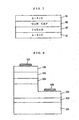
- Fig.6 shows a sixth example not forming part of the invention with an n-type AlGaN layer 72 and an InGaN layer 73 are formed in order on an n-type GaN layer 71 and a p-type SiC layer 75 is formed above the InGaN layer 73 with an undoped GaN cap layer 74 therebetween.
- the InGaN layer 73 and the GaN cap layer 74 are formed at a growth temperature of 700-950°C and the p-type SiC layer 75 is formed at a growth temperature of 1300-1500°C.
- formation of the undoped GaN cap layer 74 on the InGaN layer 73 suppresses elimination of constituent elements such as In from the InGaN layer 73.
- Fig.7 shows a seventh example not forming part of the invention with an InGaN layer 82 is formed on an n-type SiC layer 81 and a p-type SiC layer 84 is formed above the InGaN layer 82 with an undoped GaN cap layer 83 therebetween.
- the InGaN layer 82 and the undoped GaN cap layer 83 are formed at a growth temperature of 700-950°C and the p-type SiC layer 84 is formed at a growth temperature of 1300-1500°C.
- formation of the undoped GaN cap layer 83 on the InGaN layer 82 suppresses elimination of constituent elements such as In from the InGaN layer 82.
- the light emitting diodes shown in figs. 1 and 2 can be applied to light sources for use in optical fiber communication systems, light sources for use in photocouplers, monochromatic or polychromatic pilot lamps, light sources for use in display devices such as digital displays, level meters and displays, light sources for use in facsimile devices, printer heads, signal lamps, lamps for use in automobiles such as high-beam lamps, liquid-crystal televisions, back-light sources for use in liquid-crystal displays, amusement systems, and so on.
- the semiconductor laser devices shown in figs. 3 to 5 can be applied to laser surgical knives, light sources for use in optical communication systems, light sources for use in optical pick-up devices in disk systems for DVD (Digital Video Disk) and the like, light sources for use in color laser beam printers, light sources for use in laser processing devices, light sources for laser holographies, light sources for laser displays, light sources for amusement systems, and so on.
Landscapes
- Physics & Mathematics (AREA)
- Condensed Matter Physics & Semiconductors (AREA)
- General Physics & Mathematics (AREA)
- Electromagnetism (AREA)
- Optics & Photonics (AREA)
- Geometry (AREA)
- Led Devices (AREA)
- Semiconductor Lasers (AREA)
Claims (16)
- Licht emittierende Vorrichtung, umfassend in der folgenden Reihenfolge:eine Pufferschicht;eine Unterschicht aus GaN oder AlGaN;eine erste Überzugsschicht aus einem Verbundhalbleiter eines ersten Leitfähigkeitstyps auf Nitridbasis;eine aktive Schicht, die aus einem Indium enthaltenden Verbundhalbleiter auf Nitridbasis besteht; undeine zweite Überzugsschicht aus einem Verbundhalbleiter eines zweiten Leitfähigkeitstyps auf Nitridbasis,
dadurch gekennzeichnet, dass die Pufferschicht aus AlGaN besteht und eine Deckschicht aus AlGaN auf der aktiven Schicht bereitgestellt ist. - Licht emittierende Vorrichtung nach Anspruch 1, wobei die Unterschicht eine undotierte Schicht ist.
- Licht emittierende Vorrichtung nach Anspruch 1, die weiters eine Kontaktschicht aus GaN des ersten Leitfähigkeitstyps umfasst, die in Ohmschem Kontakt mit einer Elektrode ist und zwischen der Unterschicht und der ersten Überzugsschicht angeordnet ist.
- Licht emittierende Vorrichtung nach Anspruch 1, wobei die aktive Schicht eine Quantenquellstruktur aufweist, die eine Quantenquellschicht umfasst.
- Licht emittierende Vorrichtung nach Anspruch 1, wobei die Deckschicht eine Bandlücke aufweist, die größer als die der aktiven Schicht ist und zwischen jener der aktiven Schicht und der zweiten Überzugsschicht liegt.
- Licht emittierende Vorrichtung nach Anspruch 1, wobei die Deckschicht eine Verunreinigungskonzentration aufweist, die geringer ist als die der zweiten Überzugsschicht.
- Licht emittierende Vorrichtung nach Anspruch 1, wobei die Pufferschicht nicht einkristallin ist.
- Licht emittierende Vorrichtung nach Anspruch 1, wobei die Unterschicht einkristallin ist.
- Verfahren zur Herstellung einer Licht emittierenden Vorrichtung, das die nachstehenden Schritte in der folgenden Reihenfolge umfasst:Ausbilden einer Pufferschicht,Ausbilden einer Unterschicht aus GaN oder AlGaN;Ausbilden einer ersten Überzugsschicht aus einem Verbundhalbleiter eines ersten Leitfähigkeitstyps auf Nitridbasis;Ausbilden einer aktiven Schicht, die aus einem Indium enthaltenden Verbundhalbleiter auf Nitridbasis besteht; undAusbilden einer zweiten Überzugsschicht aus einem Verbundhalbleiter eines zweiten Leitfähigkeitstyps auf Nitridbasis bei einer höheren Wachstumstemperatur als der der aktiven Schicht,dadurch gekennzeichnet, dass die Pufferschicht aus AlGaN besteht und eine Deckschicht aus AlGaN auf der aktiven Schicht ausgebildet wird.
- Verfahren nach Anspruch 9, das weiters den Schritt des Ausbildens einer Kontaktschicht aus GaN des ersten Leitfähigkeitstyps, die in Ohmschen Kontakt mit einer Elektrode kommt, auf der Unterschicht umfasst.
- Verfahren nach Anspruch 10, wobei der Schritt des Ausbildens der Kontaktschicht des ersten Leitfähigkeitstyps, die in Ohmschen Kontakt mit einer Elektrode kommt, das Ausbilden der Kontaktschicht des ersten Leitfähigkeitstyps bei einer Wachstumstemperatur von nicht weniger als 1000 °C und nicht mehr als 1200 °C umfasst.
- Verfahren nach Anspruch 9, wobei der Schritt des Ausbildens der aktiven Schicht das Ausbilden einer Quantenquellstruktur umfasst, die eine Quantenquellschicht umfasst.
- Verfahren nach Anspruch 9, wobei der Schritt des Ausbildens der aktiven Schicht das Ausbilden der aktiven Schicht bei einer Wachstumstemperatur von nicht weniger als 700 °C und nicht mehr als 950 °C umfasst.
- Verfahren nach Anspruch 9, wobei der Schritt des Ausbildens der zweiten Überzugsschicht das Ausbilden der zweiten Überzugsschicht bei einer Wachstumstemperatur von nicht weniger als 1000 °C und nicht mehr als 1200 °C umfasst.
- Verfahren nach Anspruch 9, wobei der Schritt des Ausbildens der Deckschicht das Ausbilden der Deckschicht bei einer Wachstumstemperatur gleich der oder niedriger als die der aktiven Schicht umfasst.
- Verfahren nach Anspruch 9, wobei der Schritt des Ausbildens der Deckschicht das Ausbilden der Deckschicht bei einer Wachstumstemperatur von nicht weniger als 700 °C und nicht mehr als 950 °C umfasst.
Priority Applications (1)
| Application Number | Priority Date | Filing Date | Title |
|---|---|---|---|
| EP11174758.0A EP2383846B1 (de) | 1996-04-26 | 1997-04-07 | Lichtemissionsvorrichtung und Herstellungsverfahren dafür |
Applications Claiming Priority (5)
| Application Number | Priority Date | Filing Date | Title |
|---|---|---|---|
| JP10783396 | 1996-04-26 | ||
| JP10783396 | 1996-04-26 | ||
| JP05522197A JP3448450B2 (ja) | 1996-04-26 | 1997-03-10 | 発光素子およびその製造方法 |
| JP5522197 | 1997-03-10 | ||
| EP97302374A EP0803916B1 (de) | 1996-04-26 | 1997-04-07 | Herstellungsverfahren einer Lichtemittierende Vorrichtung |
Related Parent Applications (1)
| Application Number | Title | Priority Date | Filing Date |
|---|---|---|---|
| EP97302374A Division EP0803916B1 (de) | 1996-04-26 | 1997-04-07 | Herstellungsverfahren einer Lichtemittierende Vorrichtung |
Related Child Applications (2)
| Application Number | Title | Priority Date | Filing Date |
|---|---|---|---|
| EP11174758.0A Division-Into EP2383846B1 (de) | 1996-04-26 | 1997-04-07 | Lichtemissionsvorrichtung und Herstellungsverfahren dafür |
| EP11174758.0A Division EP2383846B1 (de) | 1996-04-26 | 1997-04-07 | Lichtemissionsvorrichtung und Herstellungsverfahren dafür |
Publications (2)
| Publication Number | Publication Date |
|---|---|
| EP1453112A1 EP1453112A1 (de) | 2004-09-01 |
| EP1453112B1 true EP1453112B1 (de) | 2015-07-08 |
Family
ID=26396092
Family Applications (3)
| Application Number | Title | Priority Date | Filing Date |
|---|---|---|---|
| EP11174758.0A Expired - Lifetime EP2383846B1 (de) | 1996-04-26 | 1997-04-07 | Lichtemissionsvorrichtung und Herstellungsverfahren dafür |
| EP97302374A Expired - Lifetime EP0803916B1 (de) | 1996-04-26 | 1997-04-07 | Herstellungsverfahren einer Lichtemittierende Vorrichtung |
| EP04011150.2A Expired - Lifetime EP1453112B1 (de) | 1996-04-26 | 1997-04-07 | Lichtemittierende Vorrichtung und dessen Herstellungsverfahren |
Family Applications Before (2)
| Application Number | Title | Priority Date | Filing Date |
|---|---|---|---|
| EP11174758.0A Expired - Lifetime EP2383846B1 (de) | 1996-04-26 | 1997-04-07 | Lichtemissionsvorrichtung und Herstellungsverfahren dafür |
| EP97302374A Expired - Lifetime EP0803916B1 (de) | 1996-04-26 | 1997-04-07 | Herstellungsverfahren einer Lichtemittierende Vorrichtung |
Country Status (6)
| Country | Link |
|---|---|
| US (3) | US5990496A (de) |
| EP (3) | EP2383846B1 (de) |
| JP (1) | JP3448450B2 (de) |
| KR (1) | KR100500331B1 (de) |
| CN (2) | CN100353573C (de) |
| DE (1) | DE69735078T2 (de) |
Families Citing this family (65)
| Publication number | Priority date | Publication date | Assignee | Title |
|---|---|---|---|---|
| JP3448450B2 (ja) * | 1996-04-26 | 2003-09-22 | 三洋電機株式会社 | 発光素子およびその製造方法 |
| US5987048A (en) * | 1996-07-26 | 1999-11-16 | Kabushiki Kaisha Toshiba | Gallium nitride-based compound semiconductor laser and method of manufacturing the same |
| WO1999038218A1 (fr) * | 1998-01-21 | 1999-07-29 | Rohm Co., Ltd. | Element luminescent a semiconducteur et procede de fabrication |
| TW413972B (en) * | 1998-04-22 | 2000-12-01 | Matsushita Electric Industrial Co Ltd | Semiconductor laser device |
| JP4214585B2 (ja) * | 1998-04-24 | 2009-01-28 | 富士ゼロックス株式会社 | 半導体デバイス、半導体デバイスの製造方法及び製造装置 |
| JP2000031533A (ja) | 1998-07-14 | 2000-01-28 | Toshiba Corp | 半導体発光素子 |
| US6459100B1 (en) * | 1998-09-16 | 2002-10-01 | Cree, Inc. | Vertical geometry ingan LED |
| JP3804335B2 (ja) * | 1998-11-26 | 2006-08-02 | ソニー株式会社 | 半導体レーザ |
| US6316332B1 (en) | 1998-11-30 | 2001-11-13 | Lo Yu-Hwa | Method for joining wafers at a low temperature and low stress |
| KR100486699B1 (ko) * | 1999-02-12 | 2005-05-03 | 삼성전자주식회사 | p형 GaN 단결정 성장 방법 |
| DE60043536D1 (de) | 1999-03-04 | 2010-01-28 | Nichia Corp | Nitridhalbleiterlaserelement |
| WO2000054342A1 (en) * | 1999-03-10 | 2000-09-14 | Nova Crystals, Inc. | HIGH BRIGHTNESS NITRIDE-BASED LEDs |
| JP3459588B2 (ja) * | 1999-03-24 | 2003-10-20 | 三洋電機株式会社 | 半導体レーザ素子の製造方法 |
| JP3786544B2 (ja) * | 1999-06-10 | 2006-06-14 | パイオニア株式会社 | 窒化物半導体素子の製造方法及びかかる方法により製造された素子 |
| JP4032636B2 (ja) * | 1999-12-13 | 2008-01-16 | 日亜化学工業株式会社 | 発光素子 |
| JP2001244551A (ja) * | 2000-02-28 | 2001-09-07 | Sony Corp | パルセーションレーザ |
| US6731663B1 (en) * | 2000-03-28 | 2004-05-04 | The Furukawa Electric Co., Ltd. | Ridge waveguide type semiconductor laser device |
| KR100506077B1 (ko) * | 2000-04-15 | 2005-08-04 | 삼성전기주식회사 | 유기금속기상화학증착법에 의한 고품위 ⅲ-족 질화물 박막성장 방법 |
| JP5145617B2 (ja) * | 2000-07-03 | 2013-02-20 | 日亜化学工業株式会社 | n型窒化物半導体積層体およびそれを用いる半導体素子 |
| US6586762B2 (en) | 2000-07-07 | 2003-07-01 | Nichia Corporation | Nitride semiconductor device with improved lifetime and high output power |
| KR100550158B1 (ko) * | 2000-09-21 | 2006-02-08 | 샤프 가부시키가이샤 | 질화물 반도체 발광소자 및 그것을 포함한 광학장치 |
| US6653662B2 (en) | 2000-11-01 | 2003-11-25 | Matsushita Electric Industrial Co., Ltd. | Semiconductor light-emitting device, method for fabricating the same, and method for driving the same |
| JP4963763B2 (ja) * | 2000-12-21 | 2012-06-27 | 日本碍子株式会社 | 半導体素子 |
| JP3864735B2 (ja) | 2000-12-28 | 2007-01-10 | ソニー株式会社 | 半導体発光素子およびその製造方法 |
| US6800876B2 (en) | 2001-01-16 | 2004-10-05 | Cree, Inc. | Group III nitride LED with undoped cladding layer (5000.137) |
| USRE46589E1 (en) | 2001-01-16 | 2017-10-24 | Cree, Inc. | Group III nitride LED with undoped cladding layer and multiple quantum well |
| CA2444273C (en) | 2001-04-12 | 2012-05-22 | Nichia Corporation | Gallium nitride semiconductor device |
| JP3819730B2 (ja) * | 2001-05-11 | 2006-09-13 | 三洋電機株式会社 | 窒化物系半導体素子および窒化物半導体の形成方法 |
| US6958497B2 (en) | 2001-05-30 | 2005-10-25 | Cree, Inc. | Group III nitride based light emitting diode structures with a quantum well and superlattice, group III nitride based quantum well structures and group III nitride based superlattice structures |
| US6977953B2 (en) * | 2001-07-27 | 2005-12-20 | Sanyo Electric Co., Ltd. | Nitride-based semiconductor light-emitting device and method of fabricating the same |
| JP2003140100A (ja) * | 2001-11-01 | 2003-05-14 | Oki Electric Ind Co Ltd | 導波路型光素子、これを用いた集積化光導波路素子、及びその製造方法 |
| KR100597532B1 (ko) | 2001-11-05 | 2006-07-10 | 니치아 카가쿠 고교 가부시키가이샤 | 반도체 소자 |
| US6683327B2 (en) * | 2001-11-13 | 2004-01-27 | Lumileds Lighting U.S., Llc | Nucleation layer for improved light extraction from light emitting devices |
| US6665329B1 (en) * | 2002-06-06 | 2003-12-16 | Sandia Corporation | Broadband visible light source based on AllnGaN light emitting diodes |
| US6900067B2 (en) * | 2002-12-11 | 2005-05-31 | Lumileds Lighting U.S., Llc | Growth of III-nitride films on mismatched substrates without conventional low temperature nucleation layers |
| US6952024B2 (en) * | 2003-02-13 | 2005-10-04 | Cree, Inc. | Group III nitride LED with silicon carbide cladding layer |
| JP3767863B2 (ja) * | 2003-12-18 | 2006-04-19 | ローム株式会社 | 半導体発光素子およびその製法 |
| WO2005086088A1 (en) | 2004-03-04 | 2005-09-15 | Semiconductor Energy Laboratory Co., Ltd. | Id chip and ic card |
| US9524869B2 (en) | 2004-03-11 | 2016-12-20 | Epistar Corporation | Nitride-based semiconductor light-emitting device |
| JP2005268581A (ja) * | 2004-03-19 | 2005-09-29 | Matsushita Electric Ind Co Ltd | 窒化ガリウム系化合物半導体発光素子 |
| US7777241B2 (en) * | 2004-04-15 | 2010-08-17 | The Trustees Of Boston University | Optical devices featuring textured semiconductor layers |
| US8035113B2 (en) * | 2004-04-15 | 2011-10-11 | The Trustees Of Boston University | Optical devices featuring textured semiconductor layers |
| KR101365604B1 (ko) * | 2004-05-10 | 2014-02-20 | 더 리전트 오브 더 유니버시티 오브 캘리포니아 | 유기금속 화학기상증착법을 이용한 비극성 질화인듐갈륨 박막들, 이중 구조들 및 소자들의 제조 |
| US7504274B2 (en) | 2004-05-10 | 2009-03-17 | The Regents Of The University Of California | Fabrication of nonpolar indium gallium nitride thin films, heterostructures and devices by metalorganic chemical vapor deposition |
| KR100611491B1 (ko) | 2004-08-26 | 2006-08-10 | 엘지이노텍 주식회사 | 질화물 반도체 발광소자 및 그 제조방법 |
| US20070069225A1 (en) * | 2005-09-27 | 2007-03-29 | Lumileds Lighting U.S., Llc | III-V light emitting device |
| JP5068020B2 (ja) * | 2006-02-20 | 2012-11-07 | シャープ株式会社 | 窒化物半導体発光素子の製造方法 |
| JP5047508B2 (ja) | 2006-02-27 | 2012-10-10 | シャープ株式会社 | 窒化物半導体発光素子の製造方法 |
| JP2009152552A (ja) * | 2007-12-18 | 2009-07-09 | Seoul Opto Devices Co Ltd | 多重量子井戸構造の活性領域を有する発光ダイオード |
| US8592800B2 (en) * | 2008-03-07 | 2013-11-26 | Trustees Of Boston University | Optical devices featuring nonpolar textured semiconductor layers |
| JP2010123920A (ja) * | 2008-10-20 | 2010-06-03 | Sumitomo Electric Ind Ltd | 窒化物系半導体発光素子を作製する方法、及びエピタキシャルウエハを作製する方法 |
| US8536615B1 (en) | 2009-12-16 | 2013-09-17 | Cree, Inc. | Semiconductor device structures with modulated and delta doping and related methods |
| US8604461B2 (en) | 2009-12-16 | 2013-12-10 | Cree, Inc. | Semiconductor device structures with modulated doping and related methods |
| CN102034912B (zh) * | 2009-12-29 | 2015-03-25 | 比亚迪股份有限公司 | 发光二极管外延片、其制作方法及芯片的制作方法 |
| US8575592B2 (en) * | 2010-02-03 | 2013-11-05 | Cree, Inc. | Group III nitride based light emitting diode structures with multiple quantum well structures having varying well thicknesses |
| JP5372045B2 (ja) | 2011-02-25 | 2013-12-18 | 株式会社東芝 | 半導体発光素子 |
| US9781783B2 (en) | 2011-04-15 | 2017-10-03 | Semiconductor Energy Laboratory Co., Ltd. | Light-emitting device, display device, light-emitting system, and display system |
| US11966810B2 (en) | 2012-02-06 | 2024-04-23 | Cognex Corporation | System and method for expansion of field of view in a vision system |
| US8646690B2 (en) | 2012-02-06 | 2014-02-11 | Cognex Corporation | System and method for expansion of field of view in a vision system |
| US9892298B2 (en) | 2012-02-06 | 2018-02-13 | Cognex Corporation | System and method for expansion of field of view in a vision system |
| JP5651758B2 (ja) * | 2013-10-08 | 2015-01-14 | 株式会社東芝 | 半導体発光素子 |
| KR102223037B1 (ko) | 2014-10-01 | 2021-03-05 | 삼성전자주식회사 | 반도체 발광소자 제조방법 |
| CN109417274B (zh) * | 2016-06-30 | 2021-12-07 | 新唐科技日本株式会社 | 半导体激光装置、半导体激光模块及熔接用激光光源系统 |
| JP7137556B2 (ja) * | 2017-03-16 | 2022-09-14 | ヌヴォトンテクノロジージャパン株式会社 | 半導体レーザ装置、半導体レーザモジュール、溶接用レーザ光源システム、及び、半導体レーザ装置の製造方法 |
| CN108538978A (zh) * | 2018-04-13 | 2018-09-14 | 厦门乾照光电股份有限公司 | 一种可提高发光效率的led外延结构及其生长方法 |
Family Cites Families (56)
| Publication number | Priority date | Publication date | Assignee | Title |
|---|---|---|---|---|
| JPH088390B2 (ja) | 1984-11-30 | 1996-01-29 | 三洋電機株式会社 | 半導体レーザ |
| JP3160914B2 (ja) | 1990-12-26 | 2001-04-25 | 豊田合成株式会社 | 窒化ガリウム系化合物半導体レーザダイオード |
| US5290393A (en) * | 1991-01-31 | 1994-03-01 | Nichia Kagaku Kogyo K.K. | Crystal growth method for gallium nitride-based compound semiconductor |
| JPH088217B2 (ja) * | 1991-01-31 | 1996-01-29 | 日亜化学工業株式会社 | 窒化ガリウム系化合物半導体の結晶成長方法 |
| JP2791448B2 (ja) | 1991-04-19 | 1998-08-27 | 日亜化学工業 株式会社 | 発光ダイオード |
| US5495155A (en) | 1991-06-28 | 1996-02-27 | United Technologies Corporation | Device in a power delivery circuit |
| JPH05291686A (ja) * | 1992-04-14 | 1993-11-05 | Matsushita Electric Ind Co Ltd | 半導体レーザ |
| JP3243768B2 (ja) | 1992-07-06 | 2002-01-07 | 日本電信電話株式会社 | 半導体発光素子 |
| JP2875437B2 (ja) | 1992-07-30 | 1999-03-31 | シャープ株式会社 | 半導体発光素子およびその製造方法 |
| JP2999638B2 (ja) * | 1992-10-28 | 2000-01-17 | 日本電信電話株式会社 | 仮想体験システム |
| US5578839A (en) * | 1992-11-20 | 1996-11-26 | Nichia Chemical Industries, Ltd. | Light-emitting gallium nitride-based compound semiconductor device |
| JPH06164055A (ja) * | 1992-11-25 | 1994-06-10 | Asahi Chem Ind Co Ltd | 量子井戸型半導体レーザ |
| JP3091593B2 (ja) | 1993-01-14 | 2000-09-25 | 日亜化学工業株式会社 | 窒化物半導体発光デバイス用積層体 |
| JP3761589B2 (ja) * | 1993-03-26 | 2006-03-29 | 豊田合成株式会社 | 窒化ガリウム系化合物半導体発光素子 |
| DE69433926T2 (de) * | 1993-04-28 | 2005-07-21 | Nichia Corp., Anan | Halbleitervorrichtung aus einer galliumnitridartigen III-V-Halbleiterverbindung |
| JPH0774431A (ja) * | 1993-06-23 | 1995-03-17 | Furukawa Electric Co Ltd:The | 半導体光素子 |
| US5583878A (en) * | 1993-06-23 | 1996-12-10 | The Furukawa Electric Co., Ltd. | Semiconductor optical device |
| JP2785254B2 (ja) | 1993-06-28 | 1998-08-13 | 日亜化学工業株式会社 | 窒化ガリウム系化合物半導体発光素子 |
| JPH0750410A (ja) * | 1993-08-06 | 1995-02-21 | Hitachi Ltd | 半導体結晶積層体及びその形成方法並びに半導体装置 |
| JPH07106698A (ja) * | 1993-09-29 | 1995-04-21 | Sony Corp | 半導体発光素子 |
| JPH07267796A (ja) | 1994-03-31 | 1995-10-17 | Mitsubishi Cable Ind Ltd | GaN単結晶の製造方法 |
| DE69431333T2 (de) | 1993-10-08 | 2003-07-31 | Mitsubishi Cable Industries, Ltd. | GaN-Einkristall |
| JP3297220B2 (ja) | 1993-10-29 | 2002-07-02 | 株式会社東芝 | 半導体装置の製造方法および半導体装置 |
| JP2932468B2 (ja) | 1993-12-10 | 1999-08-09 | 日亜化学工業株式会社 | 窒化ガリウム系化合物半導体発光素子 |
| US5393993A (en) * | 1993-12-13 | 1995-02-28 | Cree Research, Inc. | Buffer structure between silicon carbide and gallium nitride and resulting semiconductor devices |
| JPH07235723A (ja) | 1994-02-23 | 1995-09-05 | Hitachi Ltd | 半導体レーザ素子 |
| JP3509260B2 (ja) | 1994-03-08 | 2004-03-22 | 住友化学工業株式会社 | 3−5族化合物半導体と発光素子 |
| US5656832A (en) * | 1994-03-09 | 1997-08-12 | Kabushiki Kaisha Toshiba | Semiconductor heterojunction device with ALN buffer layer of 3nm-10nm average film thickness |
| JP3325380B2 (ja) * | 1994-03-09 | 2002-09-17 | 株式会社東芝 | 半導体発光素子およびその製造方法 |
| JPH0818159A (ja) * | 1994-04-25 | 1996-01-19 | Hitachi Ltd | 半導体レーザ素子及びその作製方法 |
| JP2956489B2 (ja) * | 1994-06-24 | 1999-10-04 | 日亜化学工業株式会社 | 窒化ガリウム系化合物半導体の結晶成長方法 |
| US5592501A (en) * | 1994-09-20 | 1997-01-07 | Cree Research, Inc. | Low-strain laser structures with group III nitride active layers |
| US5777350A (en) | 1994-12-02 | 1998-07-07 | Nichia Chemical Industries, Ltd. | Nitride semiconductor light-emitting device |
| US5679965A (en) * | 1995-03-29 | 1997-10-21 | North Carolina State University | Integrated heterostructures of Group III-V nitride semiconductor materials including epitaxial ohmic contact, non-nitride buffer layer and methods of fabricating same |
| JP3728332B2 (ja) * | 1995-04-24 | 2005-12-21 | シャープ株式会社 | 化合物半導体発光素子 |
| JPH0997921A (ja) | 1995-07-21 | 1997-04-08 | Sumitomo Chem Co Ltd | 3−5族化合物半導体の製造方法 |
| JPH0955221A (ja) | 1995-08-10 | 1997-02-25 | Tanaka Kikinzoku Kogyo Kk | 燃料電池用プレート、燃料電池ユニット及び積層型燃料電池 |
| JPH0964419A (ja) | 1995-08-28 | 1997-03-07 | Sumitomo Chem Co Ltd | 3−5族化合物半導体及び発光素子 |
| EP0762516B1 (de) * | 1995-08-28 | 1999-04-21 | Mitsubishi Cable Industries, Ltd. | Lichtemittierende Vorrichtung auf Basis einer Nitridverbindung der Gruppe III |
| JP3658112B2 (ja) | 1995-11-06 | 2005-06-08 | 日亜化学工業株式会社 | 窒化物半導体レーザダイオード |
| JP3235440B2 (ja) | 1995-11-24 | 2001-12-04 | 日亜化学工業株式会社 | 窒化物半導体レーザ素子とその製造方法 |
| JP2900990B2 (ja) | 1995-11-24 | 1999-06-02 | 日亜化学工業株式会社 | 窒化物半導体発光素子 |
| CN100350641C (zh) | 1995-11-06 | 2007-11-21 | 日亚化学工业株式会社 | 氮化物半导体器件 |
| JPH09186363A (ja) | 1995-12-27 | 1997-07-15 | Toshiba Corp | 半導体発光素子及びその製造方法 |
| JPH09199798A (ja) | 1996-01-18 | 1997-07-31 | Nichia Chem Ind Ltd | 窒化物半導体レーザ素子 |
| EP0817283A1 (de) | 1996-01-19 | 1998-01-07 | Matsushita Electric Industrial Co., Ltd. | Lichtemittierende vorrichtung aus einer gallium-nitrid-halbleiterverbindung und verfahren zum herstellen einer gallium-nitrid-halbleiterverbindung |
| JPH09232680A (ja) | 1996-02-22 | 1997-09-05 | Matsushita Electric Ind Co Ltd | 半導体発光素子及びその製造方法 |
| US5903017A (en) | 1996-02-26 | 1999-05-11 | Kabushiki Kaisha Toshiba | Compound semiconductor device formed of nitrogen-containing gallium compound such as GaN, AlGaN or InGaN |
| JP3441329B2 (ja) | 1996-02-26 | 2003-09-02 | 株式会社東芝 | 窒化ガリウム系半導体素子 |
| JP3754120B2 (ja) | 1996-02-27 | 2006-03-08 | 株式会社東芝 | 半導体発光装置 |
| JP3399216B2 (ja) | 1996-03-14 | 2003-04-21 | ソニー株式会社 | 半導体発光素子 |
| US6072818A (en) | 1996-03-28 | 2000-06-06 | Fuji Photo Film Co., Ltd. | Semiconductor light emission device |
| JPH09266352A (ja) | 1996-03-28 | 1997-10-07 | Fuji Photo Film Co Ltd | 半導体発光素子 |
| JP3441883B2 (ja) | 1996-04-17 | 2003-09-02 | 日亜化学工業株式会社 | 窒化物半導体レーザ素子 |
| JP3448450B2 (ja) * | 1996-04-26 | 2003-09-22 | 三洋電機株式会社 | 発光素子およびその製造方法 |
| JP3778609B2 (ja) | 1996-04-26 | 2006-05-24 | 三洋電機株式会社 | 半導体素子の製造方法 |
-
1997
- 1997-03-10 JP JP05522197A patent/JP3448450B2/ja not_active Expired - Lifetime
- 1997-04-07 EP EP11174758.0A patent/EP2383846B1/de not_active Expired - Lifetime
- 1997-04-07 DE DE69735078T patent/DE69735078T2/de not_active Expired - Lifetime
- 1997-04-07 EP EP97302374A patent/EP0803916B1/de not_active Expired - Lifetime
- 1997-04-07 EP EP04011150.2A patent/EP1453112B1/de not_active Expired - Lifetime
- 1997-04-25 CN CNB2004100434632A patent/CN100353573C/zh not_active Expired - Lifetime
- 1997-04-25 KR KR1019970015615A patent/KR100500331B1/ko not_active Expired - Lifetime
- 1997-04-25 CN CNB971108064A patent/CN1220278C/zh not_active Expired - Lifetime
- 1997-04-25 US US08/847,471 patent/US5990496A/en not_active Expired - Lifetime
-
1999
- 1999-10-27 US US09/427,694 patent/US6162656A/en not_active Ceased
-
2002
- 2002-12-18 US US10/321,516 patent/USRE42074E1/en not_active Expired - Lifetime
Also Published As
| Publication number | Publication date |
|---|---|
| JPH1012923A (ja) | 1998-01-16 |
| EP1453112A1 (de) | 2004-09-01 |
| EP2383846A2 (de) | 2011-11-02 |
| JP3448450B2 (ja) | 2003-09-22 |
| DE69735078T2 (de) | 2006-08-24 |
| US6162656A (en) | 2000-12-19 |
| CN1540775A (zh) | 2004-10-27 |
| DE69735078D1 (de) | 2006-04-06 |
| EP0803916A3 (de) | 2000-03-08 |
| US5990496A (en) | 1999-11-23 |
| CN100353573C (zh) | 2007-12-05 |
| KR100500331B1 (ko) | 2005-09-30 |
| EP2383846B1 (de) | 2020-02-19 |
| CN1220278C (zh) | 2005-09-21 |
| EP0803916A2 (de) | 1997-10-29 |
| KR970072575A (ko) | 1997-11-07 |
| CN1169036A (zh) | 1997-12-31 |
| USRE42074E1 (en) | 2011-01-25 |
| EP2383846A3 (de) | 2014-10-29 |
| EP0803916B1 (de) | 2006-01-11 |
Similar Documents
| Publication | Publication Date | Title |
|---|---|---|
| EP1453112B1 (de) | Lichtemittierende Vorrichtung und dessen Herstellungsverfahren | |
| US6829273B2 (en) | Nitride semiconductor layer structure and a nitride semiconductor laser incorporating a portion of same | |
| US7176479B2 (en) | Nitride compound semiconductor element | |
| EP1014455B1 (de) | Halbleitervorrichtung aus einer nitridverbindung | |
| US6690700B2 (en) | Nitride semiconductor device | |
| JP3778609B2 (ja) | 半導体素子の製造方法 | |
| EP0977279A2 (de) | AlGaInN LED und Diodenlaser | |
| EP2164115A1 (de) | Nitridhalbleiter-leuchtelement und verfahren zur herstellung eines nitridhalbleiters | |
| EP1196971B1 (de) | Nitrid-halbleiterschichtenstruktur und deren anwendung in halbleiterlasern | |
| JP5647289B2 (ja) | 発光素子の製造方法 | |
| JPH09148678A (ja) | 窒化物半導体発光素子 | |
| JP3740744B2 (ja) | 半導体の成長方法 | |
| US6191437B1 (en) | Semiconductor light emitting device and method of manufacturing the same | |
| JP2000349398A (ja) | 窒化物半導体発光素子及びその製造方法 | |
| JP3458625B2 (ja) | 半導体の成長方法 | |
| JP3371830B2 (ja) | 窒化物半導体発光素子 | |
| JP2002134787A5 (de) | ||
| JPH0955560A (ja) | 化合物半導体発光素子およびその製造方法 | |
| JP2001028473A (ja) | n型窒化物半導体の成長方法 | |
| JP3456980B2 (ja) | 化合物半導体層の形成方法 | |
| JP2000174336A (ja) | GaN系半導体発光素子およびその製造方法 |
Legal Events
| Date | Code | Title | Description |
|---|---|---|---|
| PUAI | Public reference made under article 153(3) epc to a published international application that has entered the european phase |
Free format text: ORIGINAL CODE: 0009012 |
|
| 17P | Request for examination filed |
Effective date: 20040601 |
|
| AC | Divisional application: reference to earlier application |
Ref document number: 0803916 Country of ref document: EP Kind code of ref document: P |
|
| AK | Designated contracting states |
Kind code of ref document: A1 Designated state(s): DE FR NL |
|
| AKX | Designation fees paid |
Designated state(s): DE FR NL |
|
| 17Q | First examination report despatched |
Effective date: 20110104 |
|
| RAC | Divisional application: reference to earlier application (corrected) |
Ref document number: 0803916 Country of ref document: EP Kind code of ref document: P |
|
| RIN1 | Information on inventor provided before grant (corrected) |
Inventor name: UEDA, YASUHIRO Inventor name: MATSUSHITA, YASUHIKO Inventor name: KUNISATO, TATSUYA Inventor name: KANO, TAKASHI Inventor name: YAGI, KATSUMI |
|
| RAP1 | Party data changed (applicant data changed or rights of an application transferred) |
Owner name: FUTURE LIGHT LIMITED LIABILITY COMPANY |
|
| GRAP | Despatch of communication of intention to grant a patent |
Free format text: ORIGINAL CODE: EPIDOSNIGR1 |
|
| INTG | Intention to grant announced |
Effective date: 20150130 |
|
| RIC1 | Information provided on ipc code assigned before grant |
Ipc: H01L 33/32 20100101ALI20150119BHEP Ipc: H01L 33/00 20100101AFI20150119BHEP Ipc: H01L 33/02 20100101ALI20150119BHEP Ipc: H01S 5/323 20060101ALI20150119BHEP |
|
| GRAS | Grant fee paid |
Free format text: ORIGINAL CODE: EPIDOSNIGR3 |
|
| GRAA | (expected) grant |
Free format text: ORIGINAL CODE: 0009210 |
|
| AC | Divisional application: reference to earlier application |
Ref document number: 0803916 Country of ref document: EP Kind code of ref document: P |
|
| AK | Designated contracting states |
Kind code of ref document: B1 Designated state(s): DE FR NL |
|
| REG | Reference to a national code |
Ref country code: DE Ref legal event code: R081 Ref document number: 69740793 Country of ref document: DE Owner name: SANYO ELECTRIC CO., LTD., JP Free format text: FORMER OWNER: SANYO ELECTRIC CO., LTD., MORIGUCHI-SHI, OSAKA, JP |
|
| REG | Reference to a national code |
Ref country code: DE Ref legal event code: R096 Ref document number: 69740793 Country of ref document: DE |
|
| REG | Reference to a national code |
Ref country code: NL Ref legal event code: FP |
|
| REG | Reference to a national code |
Ref country code: DE Ref legal event code: R097 Ref document number: 69740793 Country of ref document: DE |
|
| REG | Reference to a national code |
Ref country code: FR Ref legal event code: PLFP Year of fee payment: 20 |
|
| PLBE | No opposition filed within time limit |
Free format text: ORIGINAL CODE: 0009261 |
|
| STAA | Information on the status of an ep patent application or granted ep patent |
Free format text: STATUS: NO OPPOSITION FILED WITHIN TIME LIMIT |
|
| 26N | No opposition filed |
Effective date: 20160411 |
|
| PGFP | Annual fee paid to national office [announced via postgrant information from national office to epo] |
Ref country code: NL Payment date: 20160420 Year of fee payment: 20 |
|
| PGFP | Annual fee paid to national office [announced via postgrant information from national office to epo] |
Ref country code: DE Payment date: 20160421 Year of fee payment: 20 |
|
| PGFP | Annual fee paid to national office [announced via postgrant information from national office to epo] |
Ref country code: FR Payment date: 20160421 Year of fee payment: 20 |
|
| REG | Reference to a national code |
Ref country code: NL Ref legal event code: PD Owner name: SANYO ELECTRIC CO., LTD.; JP Free format text: DETAILS ASSIGNMENT: CHANGE OF OWNER(S), ASSIGNMENT; FORMER OWNER NAME: FUTURE LIGHT LIMITED LIABILITY COMPANY Effective date: 20161108 |
|
| REG | Reference to a national code |
Ref country code: DE Ref legal event code: R082 Ref document number: 69740793 Country of ref document: DE Representative=s name: LEINWEBER & ZIMMERMANN, DE Ref country code: DE Ref legal event code: R081 Ref document number: 69740793 Country of ref document: DE Owner name: SANYO ELECTRIC CO., LTD., JP Free format text: FORMER OWNER: FUTURE LIGHT LIMITED LIABILITY COMPANY, SANTA CLARA, CALIF., US |
|
| REG | Reference to a national code |
Ref country code: DE Ref legal event code: R071 Ref document number: 69740793 Country of ref document: DE |
|
| REG | Reference to a national code |
Ref country code: NL Ref legal event code: MK Effective date: 20170406 Ref country code: NL Ref legal event code: PD Owner name: EPISTAR CORPORATION; TW Free format text: DETAILS ASSIGNMENT: CHANGE OF OWNER(S), ASSIGNMENT; FORMER OWNER NAME: SANYO ELECTRIC CO., LTD. Effective date: 20170405 |
|
| REG | Reference to a national code |
Ref country code: FR Ref legal event code: TP Owner name: SANYO ELECTRIC CO., LTD., JP Effective date: 20170317 |