EP1453155B1 - Verfahren zur Herstellung von Schleifringbürsten und auf diese Weise hergestellte Schleifringbürste - Google Patents
Verfahren zur Herstellung von Schleifringbürsten und auf diese Weise hergestellte Schleifringbürste Download PDFInfo
- Publication number
- EP1453155B1 EP1453155B1 EP03026305A EP03026305A EP1453155B1 EP 1453155 B1 EP1453155 B1 EP 1453155B1 EP 03026305 A EP03026305 A EP 03026305A EP 03026305 A EP03026305 A EP 03026305A EP 1453155 B1 EP1453155 B1 EP 1453155B1
- Authority
- EP
- European Patent Office
- Prior art keywords
- circuit board
- slip ring
- brush
- printed circuit
- brush element
- Prior art date
- Legal status (The legal status is an assumption and is not a legal conclusion. Google has not performed a legal analysis and makes no representation as to the accuracy of the status listed.)
- Expired - Lifetime
Links
Images


Classifications
-
- H—ELECTRICITY
- H01—ELECTRIC ELEMENTS
- H01R—ELECTRICALLY-CONDUCTIVE CONNECTIONS; STRUCTURAL ASSOCIATIONS OF A PLURALITY OF MUTUALLY-INSULATED ELECTRICAL CONNECTING ELEMENTS; COUPLING DEVICES; CURRENT COLLECTORS
- H01R39/00—Rotary current collectors, distributors or interrupters
- H01R39/02—Details for dynamo electric machines
- H01R39/18—Contacts for co-operation with commutator or slip-ring, e.g. contact brush
- H01R39/24—Laminated contacts; Wire contacts, e.g. metallic brush, carbon fibres
-
- H—ELECTRICITY
- H01—ELECTRIC ELEMENTS
- H01R—ELECTRICALLY-CONDUCTIVE CONNECTIONS; STRUCTURAL ASSOCIATIONS OF A PLURALITY OF MUTUALLY-INSULATED ELECTRICAL CONNECTING ELEMENTS; COUPLING DEVICES; CURRENT COLLECTORS
- H01R12/00—Structural associations of a plurality of mutually-insulated electrical connecting elements, specially adapted for printed circuits, e.g. printed circuit boards [PCB], flat or ribbon cables, or like generally planar structures, e.g. terminal strips, terminal blocks; Coupling devices specially adapted for printed circuits, flat or ribbon cables, or like generally planar structures; Terminals specially adapted for contact with, or insertion into, printed circuits, flat or ribbon cables, or like generally planar structures
- H01R12/50—Fixed connections
- H01R12/51—Fixed connections for rigid printed circuits or like structures
- H01R12/55—Fixed connections for rigid printed circuits or like structures characterised by the terminals
- H01R12/57—Fixed connections for rigid printed circuits or like structures characterised by the terminals surface mounting terminals
-
- H—ELECTRICITY
- H01—ELECTRIC ELEMENTS
- H01R—ELECTRICALLY-CONDUCTIVE CONNECTIONS; STRUCTURAL ASSOCIATIONS OF A PLURALITY OF MUTUALLY-INSULATED ELECTRICAL CONNECTING ELEMENTS; COUPLING DEVICES; CURRENT COLLECTORS
- H01R39/00—Rotary current collectors, distributors or interrupters
- H01R39/02—Details for dynamo electric machines
- H01R39/38—Brush holders
- H01R39/383—Brush holders characterised by the electrical connection to the brush holder
-
- H—ELECTRICITY
- H01—ELECTRIC ELEMENTS
- H01R—ELECTRICALLY-CONDUCTIVE CONNECTIONS; STRUCTURAL ASSOCIATIONS OF A PLURALITY OF MUTUALLY-INSULATED ELECTRICAL CONNECTING ELEMENTS; COUPLING DEVICES; CURRENT COLLECTORS
- H01R43/00—Apparatus or processes specially adapted for manufacturing, assembling, maintaining, or repairing of line connectors or current collectors or for joining electric conductors
- H01R43/12—Manufacture of brushes
-
- Y—GENERAL TAGGING OF NEW TECHNOLOGICAL DEVELOPMENTS; GENERAL TAGGING OF CROSS-SECTIONAL TECHNOLOGIES SPANNING OVER SEVERAL SECTIONS OF THE IPC; TECHNICAL SUBJECTS COVERED BY FORMER USPC CROSS-REFERENCE ART COLLECTIONS [XRACs] AND DIGESTS
- Y10—TECHNICAL SUBJECTS COVERED BY FORMER USPC
- Y10T—TECHNICAL SUBJECTS COVERED BY FORMER US CLASSIFICATION
- Y10T29/00—Metal working
- Y10T29/49—Method of mechanical manufacture
- Y10T29/49002—Electrical device making
- Y10T29/49117—Conductor or circuit manufacturing
- Y10T29/49119—Brush
Definitions
- the invention relates to a method for producing slip ring brushes according to claim 1.
- the invention comprises according to claim 6, a slip ring brush itself.
- Slip ring assemblies often include a slip ring brush and slip rings, with the slip ring brush slidingly in contact with rotating slip rings during operation.
- slip ring units are used in many technical fields to transmit electrical signals or electrical power from a stationary to a rotating electrical unit. It is important that, for example, by resilient brush elements a good and lasting contact between the slip ring brush and the slip rings is given, even if, for example, the entire slip ring unit is exposed to vibrations.
- US Pat. No. 4,583,797 describes a slip ring which also has substantially U-shaped brush wires. Again, the U-shaped brush wires through a brush block, which may be formed as a printed circuit board with printed conductors inserted therethrough. The brush wires are soldered to the circuit board so that the solder joint is located on the surface of the circuit board facing the rotor.
- This design has the disadvantage that the assembly of the corresponding slip ring brush is expensive.
- slip ring brushes produced in this way have a non-optimal quality in terms of their spring properties.
- the invention is therefore an object of the invention to provide a method for producing a slip ring brush, which requires minimal installation effort, and by which high quality slip ring brushes with small space required to produce.
- a novel slip ring brush is provided by the invention, by which the life or the reliability of slip ring units is significantly increased. This is achieved by the slip ring brush according to claim 6.
- the invention is based on the idea that at least one brush element is soldered onto a first surface of a printed circuit board, wherein the soldering process is performed such that solder, coming from the second surface of the printed circuit board, passes through bores of the printed circuit board to the brush element.
- the tracks of the circuit board with the brush element are electrically and mechanically connected.
- bore is to be understood as meaning an opening or a hole, which does not necessarily have to have a circular cross-section, but may also have a polygonal cross-section or any other curve geometries as circumference boundary.
- pads are arranged on the second surface of the printed circuit board, to which the ends of a cable, with the advantage of a ribbon cable, can be electrically contacted.
- FIG. 1 shows a plan view of a first surface A of a printed circuit board 1.
- the printed circuit board 1 consists of epoxy resin, which is filled with glass fibers, and has a comparatively low thermal conductivity. Alternatively, other materials may be used for the circuit board 1, such as materials based on polyamide or ceramic components.
- FIG. 2 shows a plan view of the second surface B of the printed circuit board 1.
- the holes 1.2, 1.21, 1.22 and other conductors 1.1, 1.12 also pads 1.3, 1.31, 1.31a, 1.32, 1.32a shown.
- Parallel to the drawing plane of Figures 1 and 2 is a virtual geometric plane, namely the central longitudinal section C, which is shown in the side views of the circuit board 1 in Figures 3 and 5. Accordingly, the central longitudinal section C is located centrally between the two surfaces A and B.
- the conductor tracks 1.1, 1.11, 1.12 and the pads 1.3, 1.31, 1.31a, 1.32, 1.32a are arranged point-symmetrically with respect to the center of area P both on the surface A and on the surface B.
- this symmetry consideration applies to the center of area P for the holes 1.2, 1.21, 1.22 and the outer contour of the circuit board first
- the slip ring brush according to the invention comprises brush elements which in the example shown are designed as wire brackets 2, 21.
- the wire hanger 2, 21, which are all constructed identical, have three legs 2.1, 21.1; 2.2, 21.2; 2.3, 21.3 and have a substantially U-shaped or ⁇ -shaped, so that the wire bracket 2, 21 each have an opening 21.4.
- the wire brackets 2, 21 and their legs 2.1, 21.1; 2.2, 21.2; 2.3, 21.3 have an inside I and an outside O.
- the inside I is that geometric region of the legs 2.1, 21.1; 2.2, 21.2; 2.3, 21.3, which points to the center or center of gravity of the wire bracket 2, 21.
- the outside O from the center of the U- or ⁇ -shaped wire bracket 2, 21 away to the outside.
- the outer side O is therefore on the outer circumference of the wire bracket 2, 21.
- the wire hanger 2, 21 are made in the presented embodiment of a 20 mm long wire with a diameter of 0.2 mm by a bending process. Due to the requirements for a miniaturized as possible construction of slip ring units, the wire hanger 2, 21 a correspondingly small diameter.
- the so thin wire bracket 2, 21 have a very high volume-related surface (about 20 mm 2 / mm 3 ), whereby they assume the ambient temperature within a very short time in their entire volume.
- the wire hanger 2, 21 consist in the example shown of a noble metal alloy. This precious metal alloy contains as its main constituent the noble metal palladium with proportions of copper and silver. Alternatively, for example, as a noble metal alloy and a mixture of gold, copper and silver may be used, in which case gold can be used as the main component. In any case, the components of the alloy advantageously have a zero potential positive electrochemical potential with respect to hydrogen.
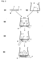
- step S3 on the surface A of the circuit board 1, the outer side O of the leg 21.1 of the wire bracket 21 is placed such that the outer side O of the leg 21.1 comes to rest at the outlet of the holes 1.21, 1.22.
- the wire bracket 21 is oriented so that, based on the central cross-section C of the circuit board 1, the opening 21.4 is located on the same side as the surface A, on which the leg 21.1 is placed.
- the respective elements are arranged in the following order: surface A, legs 21.1, opening 21.4, so that the leg 21.1 lies between the circuit board 1 and the opening 21.4.
- the leg 21.1 is placed on the surface A of the circuit board 1, that this centered on the respective outlet of the bores 1.21, 1.22 comes to rest.
- the legs 21.1 are in any case placed at the outlet of the holes 1.21, 1.22 on the circuit board 1.
- the term at the outlet of the holes 1.21, 1.22 thus includes a surface area within which an attached leg 21.1 can still be soldered by means of solder 3, which passes through the holes 1.21, 1.22 functionally.
- the printed circuit board 1 now also fulfills the function of a brush block of a slip ring brush.
- a wave soldering method can also be used, in which the legs 2.1, 21.1 of the wire clamps 2, 21 are glued to the surface A of the printed circuit board 1 before the actual soldering, wherein the wire clamps 2, 21 are again aligned so that the Opening 21.4 relative to the central longitudinal section C of the circuit board 1 is located on the same side, as the surface A and the relevant for the contacting holes 1.2, 1.21, 1.22 are covered by the legs 2.1, 21.1 of the wire bracket 2, 21, or Leg 2.1, 21.1 at the outlet of the holes 1.2, 1.21, 1.22 lie.
- the circuit board 1 is moved through a soldering machine via a transport system at a uniform speed and subjected to a wave soldering process.
- these pads 1.3, 1.31, 1.31a, 1.32, 1.32a from accepting solder, or when certain holes 1.2, 1.21, 1.22 on the printed circuit board 1 are not to be filled with solder, these pads 1.3, 1.31, 1.31 a, 1.32, 1.32a or the respective bores 1.2, 1.21, 1.22 mask off with a heat-resistant adhesive strip before the wave soldering.
- All legs 2.1, 21.1, 2.2, 21.2, 2.3, 21.3 of the wire hanger 2, 21 are thus after step S4 on one side of the circuit board 2, 21 namely on the side of the surface A.
- This arrangement has the advantage that thus the surface B of the circuit board 1 for the soldering of a cable, in the example shown a ribbon cable 5, no legs 2.1, 21.1, 2.2, 21.2, 2.3, 21.3 of the wire bracket 2, 21 are arranged, which act as geometric obstacles or interference contours for the Anlötrind processes would.
- the ribbon cable 5 has according to Figure 5 six individual wires 5.1 to 5.6 with associated insulation, while each individual wire 5.1 to 5.6 surrounded for the purpose of its identification, each with a different colored plastic insulation.
- the use of a ribbon cable 5 has, inter alia, the advantage that the sequence of the individual wires 5.1 to 5.6 is predetermined by their respective lateral connection of the plastic insulation, so that interchanging the individual wires 5.1 to 5.6 when soldering to the respective pads 1.3, 1.31, 1.31a, 1.32, 1.32a can be largely avoided.
- the stripped ends of the individual wires 5.1 to 5.6 of the ribbon cable 5 are thus soldered in step S5 to the pads 1.3, 1.31, 1.32 with a hand soldering.
- the fact that the surface B of the circuit board 1 for soldering has no geometric obstacles, the soldering can be done very quickly and a consistently high quality of the solder joints between the ends of the ribbon cable 5 and the pads 1.3, 1.31, 1.32 can be achieved.
- FIG. 4 shows a plan view of a slip ring brush according to the invention.
- the soldered to the circuit board 1 wire bracket 2, 21 out of the plane. 4 the rotor 4, consisting of six individual axially juxtaposed and mutually electrically isolated slip rings, as provided in the finished assembled slip ring unit, indicated by dashed lines.
- the ribbon cable 5 which is fixed to the surface B of the circuit board 1 is shown, wherein the concealed contours of the printed circuit board 1 of the ribbon cable 5 are shown in dashed lines.
- FIG. 5 shows a side view of the slip ring brush according to the invention, consisting of the printed circuit board 1, which serves as a brush block and the wire bracket 21, which is a brush element.
- a ribbon cable 5 is contacted according to the section Z-Z ( Figure 4).
- the outer individual wires 5.1, 5.2 are bent divergently in the region of the terminal end of the ribbon cable 5 corresponding to the pattern of the pads 1.3, 1.31, 1.32 (FIG. 2).
- the legs 21.2, 21.3 of the wire bracket 21 are shown in FIG 4 on a slip ring of the rotor 4. For proper functioning of the slip ring unit, it is necessary that always at least one of the legs 21.2, 21.3 rests against a slip ring.
- the reject rate in the manufacture of the slip ring brush or the processing time in the production be significantly reduced. Because it must be for this reason when placing a wire bracket 2, 21 only care that the right side, for example, the surface A, the circuit board 1 is selected for placement. On the other hand plays around the point P rotated by 180 ° position of the circuit board 1 no role for the subsequent functioning of the slip ring brush.
Landscapes
- Motor Or Generator Current Collectors (AREA)
- Manufacturing Of Electrical Connectors (AREA)
- Electric Connection Of Electric Components To Printed Circuits (AREA)
- Manufacturing Of Printed Wiring (AREA)
Description
- Die Erfindung betrifft ein Verfahren zur Herstellung von Schleifringbürsten gemäß dem Anspruch 1. Darüber hinaus umfasst die Erfindung, gemäß dem Anspruch 6 eine Schleifringbürste selbst.
- Schleifringeinheiten bestehen häufig unter anderem aus einer Schleifringbürste und Schleifringen, wobei die Schleifringbürste im Betrieb gleitenden Kontakt zu rotierenden Schleifringen hat. Derartige Schleifringeinheiten werden in vielen technischen Gebieten eingesetzt, um elektrische Signale oder elektrische Leistung von einer ortsfesten auf eine sich drehende elektrische Einheit zu übertragen. Dabei ist es wichtig, dass beispielsweise durch federnde Bürstenelemente ein guter und andauernder Kontakt zwischen der Schleifringbürste und den Schleifringen gegeben ist, auch wenn zum Beispiel die gesamte Schleifringeinheit Vibrationen ausgesetzt ist.
- In der Auslegeschrift DE 1 275 672 ist eine Schleifringbürste gezeigt, bei der U-förmige Bürstendrähte an einem Bürstenblock befestigt sind. Die Bürstendrähte werden im Zuge der Montage der Schleifringbürste durch den Bürstenblock hindurch geführt und durch eine Schraubverbindung am Bürstenblock festgeklemmt. Dieses Herstellungsverfahren hat unter anderem den Nachteil, dass es vergleichsweise aufwändig und zeitraubend ist.
- In der Patentschrift US 4 583 797 ist ein Schleifring beschrieben, der ebenfalls im Wesentlichen U-förmige Bürstendrähte aufweist. Auch hier sind die U-förmigen Bürstendrähte durch einen Bürstenblock, der als Leiterplatte mit Leiterbahnen ausgebildet sein kann, hindurch gesteckt. Die Bürstendrähte sind mit der Leiterplatte so verlötet, dass sich die Lötstelle an der dem Rotor zugewandten Oberfläche der Leiterplatte befindet. Diese Bauweise hat den Nachteil, dass die Montage der entsprechenden Schleifringbürste aufwändig ist. Darüber hinaus weisen derartig hergestellte Schleifringbürsten hinsichtlich ihrer Federeigenschaften eine nicht optimale Qualität auf.
- Das Dokument US-A-4143929 zeigt ebenfalls eine Schleifringbürste wie oben beschrieben.
- Der Erfindung liegt daher die Aufgabe zugrunde, ein Verfahren zur Herstellung einer Schleifringbürste zu schaffen, welches einen minimalen Montageaufwand bedingt, und durch welches qualitativ hochwertige Schleifringbürsten mit kleinem erforderlichen Bauraum herstellbar sind.
- Diese Aufgabe wird erfindungsgemäß durch die Merkmale des Anspruches 1 gelöst.
- Darüber hinaus wird durch die Erfindung eine neuartige Schleifringbürste geschaffen, durch welche die Lebensdauer bzw. die Zuverlässigkeit von Schleifringeinheiten signifikant erhöht wird. Dies wird durch die Schleifringbürste gemäß dem Anspruch 6 gelöst.
- Der Erfindung liegt der Gedanke zugrunde, dass zumindest ein Bürstenelement auf eine erste Oberfläche einer Leiterplatte gelötet wird, wobei der Lötvorgang derart vorgenommen wird, dass Lot, von der zweiten Oberfläche der Leiterplatte kommend, durch Bohrungen der Leiterplatte bis zum Bürstenelement hindurchtritt. Durch dieses Verfahren werden die Leiterbahnen der Leiterplatte mit dem Bürstenelement elektrisch und mechanisch verbunden.
- Im Folgendem ist unter dem Begriff Bohrung eine Öffnung bzw. ein Loch zu verstehen, welches nicht unbedingt einen Kreisquerschnitt aufweisen muss, vielmehr können die Bohrungen etwa auch einen Vieleckquerschnitt aufweisen oder beliebige sonstige Kurvengeometrien als Umfangsbegrenzung haben.
- In einer bevorzugten Ausgestaltung der Erfindung werden an der zweiten Oberfläche der Leiterplatte Pads angeordnet, an den die Enden eines Kabels, mit Vorteil eines Flachbandkabels, elektrisch kontaktiert werden können.
- Vorteilhafte Ausbildungen der Erfindung entnimmt man den abhängigen Ansprüchen.
- Weitere Einzelheiten und Vorteile des erfindungsgemäßen Schleifringes und des entsprechenden Verfahrens ergeben sich aus der nachfolgenden Beschreibung eines Ausführungsbeispieles anhand der beiliegenden Figuren.
- Es zeigen die
- Figur 1
- eine Draufsicht auf eine erste Oberfläche einer Leiterplatte, die als Bürstenblock dient,
- Figur 2
- eine Draufsicht auf eine zweite, der ersten gegenüber liegenden, Oberfläche der Leiterplatte,
- Figur 3
- eine schematische Darstellung von Verfahrensschritten zur Herstellung einer erfindungsgemäßen Schleifringbürste,
- Figur 4
- eine Draufsicht der Schleifringbürste mit einem Flachbandkabel,
- Figur 5
- eine Seitenansicht der Schleifringbürste mit an der Leiterplatte befestigten Bürstenelementen und einem Flachbandkabel.
- In der Figur 1 ist eine Draufsicht auf eine erste Oberfläche A einer Leiterplatte 1 dargestellt. Auf dieser Oberfläche A der Leiterplatte 1 befinden sich Leiterbahnen 1.1, 1.11 im gezeigten Beispiel aus Kupfer, die an Bohrungen 1.2, 1.21, 1.22 enden. Diese Bohrungen 1.2, 1.21, 1.22, welche die Leiterplatte 1 vollständig durchdringen, sind metallisiert, so dass sie an ihren Innenwandungen, sowie ringförmig an deren Rändern metallisch, im gezeigten Beispiel mit Zinn, beschichtet sind. Die Leiterplatte 1 besteht aus Epoxydharz, welches mit Glasfasern gefüllt ist, und weist eine vergleichsweise niedrige Wärmeleitfähigkeit auf. Alternativ dazu können auch andere Materialen für die Leiterplatte 1 verwendet werden, wie zum Beispiel Werkstoffe, die auf Polyamid- oder Keramikkomponenten basieren.
- In der Figur 2 ist eine Draufsicht auf die zweite Oberfläche B der Leiterplatte 1 gezeigt. In dieser Ansicht sind neben den Bohrungen 1.2, 1.21, 1.22 und weiteren Leiterbahnen 1.1, 1.12 auch Pads 1.3, 1.31, 1.31a, 1.32, 1.32a dargestellt. Parallel zur Zeichenebene der Figuren 1 und 2 verläuft eine virtuelle geometrische Ebene, nämlich der Mittenlängsschnitt C, welche in den Figuren 3 und 5 in den Seitenansichten der Leiterplatte 1 dargestellt ist. Demnach befindet sich der Mittenlängsschnitt C mittig zwischen den beiden Oberflächen A und B.
- Gemäß den Figuren 1 und 2, sind sowohl auf der Oberfläche A, als auch auf der Oberfläche B, die Leiterbahnen 1.1, 1.11, 1.12 als auch die Pads 1.3, 1.31, 1.31a, 1.32, 1.32a punktsymmetrisch bezüglich des Flächenmittelpunktes P angeordnet. Darüber hinaus gilt diese Symmetriebetrachtung bezüglich des Flächenmittelpunktes P auch für die Bohrungen 1.2, 1.21, 1.22 und die Außenkontur der Leiterplatte 1.
- Gemäß den Figuren 3, 4 und 5 umfasst die erfindungsgemäße Schleifringbürste Bürstenelemente, die im gezeigten Beispiel als Drahtbügel 2, 21 ausgeführt sind. Die Drahtbügel 2, 21, welche allesamt baugleich ausgeführt sind, weisen drei Schenkel 2.1, 21.1; 2.2, 21.2; 2.3, 21.3 auf und haben eine im Wesentliche U-förmige bzw. Ω-förmige Gestalt, so dass die Drahtbügel 2, 21 jeweils eine Öffnung 21.4 haben. Die Drahtbügel 2, 21 bzw. deren Schenkel 2.1, 21.1; 2.2, 21.2; 2.3, 21.3 haben eine Innenseite I und eine Außenseite O. Die Innenseite I ist derjenige geometrische Bereich der Schenkel 2.1, 21.1; 2.2, 21.2; 2.3, 21.3, der zum Mittelpunkt bzw. zum Schwerpunkt des Drahtbügels 2, 21 weist. Dagegen weist die Außenseite O vom Mittelpunkt des U- bzw. Ω-förmigen Drahtbügels 2, 21 weg nach außen. Die Außenseite O ist also am Außenumfang des Drahtbügels 2, 21.
- Die Drahtbügel 2, 21 sind im vorgestellten Ausführungsbeispiel aus einem 20 mm langen Draht mit einem Durchmesser von 0,2 mm durch ein Biegeverfahren hergestellt. Bedingt durch die Anforderungen bezüglich einer möglichst miniaturisierten Bauweise der Schleifringeinheiten weisen die Drahtbügel 2, 21 einen entsprechend geringen Durchmesser auf. Die derartig dünnen Drahtbügel 2, 21 haben eine überaus hohe volumenbezogene Oberfläche (etwa 20 mm2/mm3), wodurch sie binnen kürzester Zeit in ihrem gesamten Volumen die Umgebungstemperatur annehmen. Die Drahtbügel 2, 21 bestehen im gezeigten Beispiel aus einer Edelmetalllegierung. Diese Edelmetalllegierung weist als Hauptbestandteil das Edelmetall Palladium auf mit Anteilen von Kupfer und Silber. Alternativ dazu kann beispielsweise als Edelmetalllegierung auch eine Mischung aus Gold, Kupfer und Silber verwendet werden, wobei hier Gold als Hauptkomponente verwendet werden kann. Die Komponenten der Legierung weisen jedenfalls mit Vorteil ein in Bezug auf Wasserstoff als Nullpotential positives elektrochemisches Potenzial auf.
- Anhand der Verbindung und Kontaktierung des Drahtbügels 21 an die Leiterplatte 1 soll das Verfahren zur Herstellung der erfindungsgemäßen Schleifringbürste erläutert werden.
- Zunächst werden in dem Verfahren entsprechend der Figur 3 in den Schritten S1 und S2 die Leiterplatte 1 und ein Drahtbügel 21 bereitgestellt. Sodann wird im Schritt S3 auf die Oberfläche A der Leiterplatte 1 die Außenseite O des Schenkels 21.1 des Drahtbügels 21 derart aufgesetzt, dass die Außenseite O des Schenkels 21.1 am Austritt der Bohrungen 1.21, 1.22 zu liegen kommt. Dabei ist also der Drahtbügel 21 so ausgerichtet, dass bezogen auf den Mittenquerschnitt C der Leiterplatte 1 sich die Öffnung 21.4 auf der gleichen Seite befindet wie die Oberfläche A, an welcher der Schenkel 21.1 aufgesetzt ist. Mit anderen Worten sind ausgehend vom Mittenquerschnitt C die jeweiligen Elemente in folgender Reihenfolge angeordnet: Oberfläche A, Schenkel 21.1, Öffnung 21.4, so dass der Schenkel 21.1 zwischen der Leiterplatte 1 und der Öffnung 21.4 liegt. Im Idealfall wird der Schenkel 21.1 so auf die Oberfläche A der Leiterplatte 1 aufgesetzt, dass dieser mittig über dem jeweiligen Austritt der Bohrungen 1.21, 1.22 zu liegen kommt. In der Praxis zeigt sich jedoch, dass hier Abweichungen von ± 0,4 mm von der Mitte der Bohrungen 1.21, 1.22 toleriert werden können, ohne dass nennenswerte Qualitätseinbußen der Lötverbindung festgestellt werden. Die Schenkel 21.1 werden jedenfalls am Austritt der Bohrungen 1.21, 1.22 auf die Leiterplatte 1 aufgesetzt. Der Begriff am Austritt der Bohrungen 1.21, 1.22 umfasst also einen Flächenbereich, innerhalb welchem ein aufgesetzter Schenkel 21.1 noch mittels Lot 3, welches durch die Bohrungen 1.21, 1.22 hindurchtritt funktionsgemäß verlötet werden kann.
- Nachdem der Drahtbügel 21 bzw. dessen Schenkel 21.1 nunmehr derartig am Austritt der Bohrungen 1.21, 1.22 auf die Leiterplatte 1 aufgesetzt wurde, wird dieser im gezeigten Beispiel durch ein Handlötverfahren an der Leiterplatte 1 dauerhaft befestigt. Dabei wird das heiße Lot, bzw. das heiße Lötzinn, von der Oberfläche B der Leiterplatte 1 her in die Bohrungen 1.21, 1.22 eingeführt, so dass es infolge der Kapillarwirkung durch die Bohrungen 1.21, 1.22 und durch den Spalt zwischen den Bohrungen 1.21, 1.22 und dem Drahtbügel 21 steigt. Die Wärmequelle für den Lötprozess befindet sich also auf der dem Drahtbügel 21 gegenüberliegenden Seite der Leiterplatte 1, so dass die Leiterplatte 1 eine gegenüber dem Wärmeeintrag abschirmende Wirkung auf den Drahtbügel 21 ausübt.
- Wie bereits beschrieben, nehmen derartig filigrane Drahtbügel 2, 21 sehr rasch die Umgebungstemperatur an. Wenn nun ein Drahtbügel 2, 21 einer Temperatur, wie sie bei einem herkömmlichen Lötprozess auftritt, unmittelbar ausgesetzt würde, würde dieser ohne nennenswerten Zeitverzug vollständig durchwärmt. Eine Durchwärmung auf diesem Temperaturniveau führt aber bei den Werkstoffen, wie sie üblicherweise für die Drahtbügel 2, 21 verwendet werden, zu einer Veränderung im Werkstoffgefüge, was letztlich die elastische Verformbarkeit der Drahtbügel 2, 21 bzw. deren Federkonstante verschlechtert. Durch das erfindungsgemäße Verfahren wird also unter anderem eine temperaturschonende Behandlung der Drahtbügel 2, 21 erreicht, wenn diese an die Leiterplatte 1 gelötet werden.
- Mit dem Verfahren wird nunmehr vermieden, dass die Drahtbügel 2, 21 hohen Temperaturen ausgesetzt werden, so dass durch das Anlöten keine Beeinträchtigungen seiner Federeigenschaften, bzw. seiner Elastizität festzustellen sind, insbesondere in den Bereichen welche im Betrieb eine hohe Elastizität aufweisen müssen, nämlich die Schenkel 2.2, 21.2 und 2.3, 21.3, sowie die Übergangsbereiche von diesen Schenkeln 2.2, 21.2, 2.3, 21.3 in den Schenkel 2.1, 21.1. Mit dem gleichen Verfahren werden danach alle übrigen Drahtbügel 2, an der Leiterplatte 1 befestigt. Auf diese Weise wird durch einen Arbeitsgang, nämlich dem Lötprozess, sowohl eine elektrische Kontaktierung zwischen den Drahtbügeln 2, 21 und den Leiterbahnen 1.1, 1.11, 1.12 hergestellt, als auch eine feste mechanische Verbindung zwischen den Drahtbügeln 2, 21 und der Leiterplatte 1. Weitere Arbeitsgänge zum Befestigen der Drahtbügel 2, 21 auf der Leiterplatte 1 sind nicht zwingend notwendig, so dass mit diesem Verfahren eine überaus wirtschaftliche Herstellung von Schleifringbürsten möglich ist. Die Leiterplatte 1 erfüllt nunmehr auch die Funktion eines Bürstenblockes einer Schleifringbürste.
Alternativ zum Handlötverfahren kann auch ein Schwalllötverfahren angewendet werden, bei dem vor dem eigentlichen Löten die Schenkel 2.1, 21.1 der Drahtbügel 2, 21 auf die Oberfläche A der Leiterplatte 1 aufgeklebt werden, wobei die Drahtbügel 2, 21 wiederum so ausgerichtet werden, dass sich die Öffnung 21.4 bezogen auf den Mittenlängsschnitt C der Leiterplatte 1 auf der gleichen Seite befindet, wie die Oberfläche A und die für die Kontaktierung jeweils relevanten Bohrungen 1.2, 1.21, 1.22 von den Schenkeln 2.1, 21.1 der Drahtbügel 2, 21 abgedeckt werden, bzw. die Schenkel 2.1, 21.1 am Austritt der Bohrungen 1.2, 1.21, 1.22 liegen. Danach wird die Leiterplatte 1 über ein Transportsystem mit gleichmäßiger Geschwindigkeit durch eine Lötmaschine bewegt und einem Schwalllötverfahren ausgesetzt. Um zu verhindern, dass die Pads 1.3, 1.31, 1.31a, 1.32, 1.32a Lot annehmen, oder wenn bestimmte Bohrungen 1.2, 1.21, 1.22 auf der Leiterplatte 1 nicht mit Lot gefüllt werden sollen, kann man diese Pads 1.3, 1.31, 1.31a, 1.32, 1.32a oder die betreffende Bohrungen 1.2, 1.21, 1.22 vor dem Schwalllöten mit hitzebeständigem Klebestreifen abkleben. - Alle Schenkel 2.1, 21.1, 2.2, 21.2, 2.3, 21.3 der Drahtbügel 2, 21 befinden sich also nach dem Schritt S4 auf einer Seite der Leiterplatte 2, 21 nämlich auf der Seite der Oberfläche A. Diese Anordnung hat den Vorteil, dass somit an der Oberfläche B der Leiterplatte 1 für das Anlöten eines Kabels, im gezeigten Beispiel eines Flachbandkabels 5, keine Schenkel 2.1, 21.1, 2.2, 21.2, 2.3, 21.3 des Drahtbügels 2, 21 angeordnet sind, die als geometrische Hindernisse oder Störkonturen für den Anlötprozess wirken würden. Das Flachbandkabel 5 weist gemäß der Figur 5 sechs Einzeldrähte 5.1 bis 5.6 mit zugehöriger Isolierung auf, dabei ist jeder Einzeldraht 5.1 bis 5.6 zum Zwecke seiner Kennzeichnung mit jeweils einer unterschiedlich eingefärbten Kunststoff-Isolierung umgeben. Die Verwendung eines Flachbandkabels 5 hat unter anderem den Vorteil, dass die Reihenfolge der Einzeldrähte 5.1 bis 5.6 durch deren jeweils seitliche Verbindung der Kunststoff-Isolierung vorgegeben ist, so dass ein Vertauschen der Einzeldrähte 5.1 bis 5.6 beim Anlöten an die jeweiligen Pads 1.3, 1.31, 1.31a, 1.32, 1.32a weitgehend vermieden werden kann. Die abisolierten Enden der Einzeldrähte 5.1 bis 5.6 des Flachbandkabels 5 werden also im Schritt S5 an die Pads 1.3, 1.31, 1.32 mit einem Handlötverfahren gelötet. Dadurch, dass die Oberfläche B der Leiterplatte 1 für das Löten keine geometrischen Hindernisse aufweist, kann das Löten sehr rasch erfolgen und eine durchgehend hohe Qualität der Lötstellen zwischen den Enden des Flachbandkabels 5 und den Pads 1.3, 1.31, 1.32 erreicht werden.
- In der Figur 4 ist eine Draufsicht auf eine erfindungsgemäße Schleifringbürste gezeigt. Dabei ragen in der Darstellung die an die Leiterplatte 1 angelöteten Drahtbügel 2, 21 aus der Zeichenebene heraus. In der Figur 4 ist der Rotor 4, bestehend aus sechs einzelnen axial aneinandergereihten und gegeneinander elektrisch isolierten Schleifringen, wie er in der fertig montierten Schleifringeinheit vorgesehen ist, durch gestrichelte Linien angedeutet. Darüber hinaus ist in dieser Figur 4 auch das Flachbandkabel 5, welches an der Oberfläche B der Leiterplatte 1 befestigt ist gezeigt, wobei die von der Leiterplatte 1 verdeckten Konturen des Flachbandkabels 5 gestrichelt dargestellt sind.
- Die Figur 5 zeigt eine Seitenansicht der erfindungsgemäßen Schleifringbürste, bestehend aus der Leiterplatte 1, welche als Bürstenblock dient und dem Drahtbügel 21, der ein Bürstenelement darstellt. An der Schleifringbürste, bzw. an der Leiterplatte 1 ist ein Flachbandkabel 5 gemäß dem Schnitt Z-Z (Figur 4) kontaktiert. Die äußeren Einzeldrähte 5.1, 5.2 sind im Bereich des Anschlussendes des Flachbandkabels 5 entsprechend dem Muster der Pads 1.3, 1.31, 1.32 (Figur 2) divergierend gebogen. Die Schenkel 21.2, 21.3 des Drahtbügels 21 liegen gemäß der Figur 4 an einem Schleifring des Rotors 4 an. Für eine einwandfreie Funktion der Schleifringeinheit ist es notwendig, dass stets zumindest einer der Schenkel 21.2, 21.3 an einem Schleifring anliegt. Eine entscheidende Größe für dieses Verhalten ist die Federkonstante des Drahtbügels 21. Diese Federkonstante wurde aufgrund des thermisch schonenden Herstellungsverfahrens der Schleifringbürste nicht nachteilig beeinflusst. Es werden also durch den schleifenden Kontakt Ströme vom Rotor beispielsweise auf den Drahtbügel 21 übertragen. Über die mit Lot 3 aufgefüllten Bohrungen 1.21, 1.22 wird der Strom zur Leiterbahn 1.11, die sich auf der Oberfläche A der Leiterplatte befindet, geleitet. Durch die Kontaktierung an zwei Bohrungen 1.21, 1.22 wird einerseits sichergestellt, dass eine ausreichende mechanische Festigkeit der Verbindung gegeben ist, und andererseits wird auch eine redundante elektrische Verbindung erreicht, weil die Bohrungen 1.21, 1.22 durch die Leiterbahn 1.11 miteinander verbunden sind. Der zu übertragende Strom gelangt dann über die Leiterbahn 1.12 auf der Oberfläche B der Leiterplatte 1 zum Pad 1.32. An diesem Pad 1.32 ist ein Einzeldraht 5.2 des Flachbandkabels 5 angelötet, so dass der zu übertragene Strom in das Flachbandkabel 5 fließen kann.
- Durch die bezüglich des Punktes P symmetrische Anordnung der Bohrungen 1.2, 1.21, 1.22, Leiterbahnen 1.1, 1.11, 1.12 und Pads 1.3, 1.31, 1.31a, 1.32, 1.32a kann die Ausschussrate bei der Herstellung der Schleifringbürste bzw. die Bearbeitungszeit in der Fertigung erheblich reduziert werden. Denn es muss aus diesem Grund beim Aufsetzten eines Drahtbügels 2, 21 lediglich darauf geachtet werden, dass die richtige Seite, beispielsweise die Oberfläche A, der Leiterplatte 1 für das Aufsetzen gewählt wird. Dagegen spielt eine um den Punkt P um 180° verdrehte Lage der Leiterplatte 1 keine Rolle für die spätere Funktionsfähigkeit der Schleifringbürste.
Claims (10)
- Verfahren zur Herstellung einer Schleifringbürste umfassend· eine Leiterplatte (1), die eine erste Oberfläche (A) und eine der erste Oberfläche (A) gegenüberliegende zweite Oberfläche (B) aufweist,
mit einer Leiterbahn (1.1, 1.11, 1.12) und einer Bohrung (1.2, 1.21, 1.22), welche die Leiterplatte (1) durch die Oberfläche (A) und die Oberfläche (B) hindurch durchdringt, und· einem Bürstenelement (2, 21), welches eine Innenseite (I) und eine Außenseite (O) aufweist, wobeiein elektrischer Kontakt zwischen dem Bürstenelement (2) und der Leiterbahn (1.1, 1.11, 1.12) durch Löten hergestellt wird, dadurch gekennzeichnet dass,
vor dem Löten die Außenseite (O) des Bürstenelementes (2, 21) auf die erste Oberfläche (A) der Leiterplatte (1) aufgesetzt und so ausgerichtet wird, dass das Bürstenelement (2, 21) am Austritt der Bohrung (1.2, 1.21, 1.22) aus der ersten Oberfläche (A) der Leiterplatte (1) zu liegen kommt und weiterhin
das Bürstenelement (2, 21), in der Weise verlötet wird, dass das Lot (3), kommend von der zweiten Oberfläche (B) der Leiterplatte (1) durch die Bohrung (1.2, 1.21, 1.22) der Leiterplatte (1) bis hin zum Bürstenelement (2, 21) an der Oberfläche (A) hindurchtritt. - Verfahren gemäß dem Anspruch 1, dadurch gekennzeichnet, dass die Bohrung (1.2, 1.21, 1.22) vor dem Löten metallisiert wird.
- Verfahren gemäß dem Anspruch 1 oder 2, dadurch gekennzeichnet, dass ein Handlöt- oder ein Schwalllötprozess angewendet wird.
- Verfahren gemäß einem der vorhergehenden Ansprüche, dadurch gekennzeichnet, dass das Bürstenelement (2, 21) aus mehreren Schenkeln (2.1, 21.1, 2.2, 21.2, 2.3, 21.3) besteht.
- Verfahren gemäß einem der vorhergehenden Ansprüche, dadurch gekennzeichnet, dass auf der zweiten Oberfläche (B) der Leiterplatte (1) ein Pad (1.3, 1.31, 1.31a, 1.32, 1.32a) vorgesehen ist, an dem in einem weiteren Verfahrensschritt das Ende eines Kabels (5), insbesondere eines Flachbandkabels, kontaktiert wird (S5).
- Schleifringbürste, bestehend aus· einer Leiterplatte (1), die eine erste Oberfläche (A) und eine der erste Oberfläche (A) gegenüberliegende zweite Oberfläche (B) aufweist,
mit einer Leiterbahn (1.1, 1.11, 1.12) und einer Bohrung (1.2, 1.21, 1.22), welche die Leiterplatte (1) durch die Oberfläche (A) und die Oberfläche (B) hindurch durchdringt, und· einem Bürstenelement (2, 21), welches eine Innenseite (I) und eine Außenseite (O) aufweist, wobeidas Bürstenelement (2) und die Leiterbahn (1.1, 1.11, 1.12) durch eine Lötverbindung in elektrischem Kontakt stehen, dadurch gekennzeichnet dass,
das Bürstenelement (2, 21), in der Weise verlötet ist, dass an der Lötverbindung die Außenseite (O) des Bürstenelementes (2, 21) zur ersten Oberfläche (A) der Leiterplatte (1) weist und dass das Lot (3), von der zweiten Oberfläche (B) der Leiterplatte (1) durch die Bohrung (1.2, 1.21, 1.22) der Leiterplatte (1) bis hin zum Bürstenelement (2, 21) an der Oberfläche (A) hindurchgetreten ist. - Schleifringbürste, gemäß dem Anspruch 6, dadurch gekennzeichnet, dass das Bürstenelement (2, 21) U-förmig ausgestaltet ist und mehrere Schenkel (2.1, 21.1, 2.2, 21.2, 2.3, 21.3) umfasst.
- Schleifringbürste gemäß einem der Ansprüche 6 oder 7, dadurch gekennzeichnet, dass das Bürstenelement (2, 21) aus einer Edelmetalllegierung besteht.
- Schleifringbürste gemäß einem der Ansprüche 6 bis 8, dadurch gekennzeichnet, dass die Bohrung (1.2, 1.21, 1.22) metallisiert ist.
- Schleifringbürste gemäß einem der Ansprüche 6 bis 9, dadurch gekennzeichnet, dass auf der zweiten Oberfläche (B) der Leiterplatte (1) ein Pad (1.3, 1.31, 1.31 a, 1.32, 1.32a) vorgesehen ist, an dem das Ende eines Kabels (5), insbesondere eines Flachbandkabels, kontaktierbar ist.
Applications Claiming Priority (4)
| Application Number | Priority Date | Filing Date | Title |
|---|---|---|---|
| DE10309213 | 2003-02-28 | ||
| DE10309213 | 2003-02-28 | ||
| DE10324699A DE10324699A1 (de) | 2003-02-28 | 2003-05-30 | Verfahren zur Herstellung von Schleifringbürsten und auf diese WEise hergestellte Schleifringbürste |
| DE10324699 | 2003-05-30 |
Publications (3)
| Publication Number | Publication Date |
|---|---|
| EP1453155A2 EP1453155A2 (de) | 2004-09-01 |
| EP1453155A3 EP1453155A3 (de) | 2005-10-26 |
| EP1453155B1 true EP1453155B1 (de) | 2007-03-07 |
Family
ID=32773175
Family Applications (1)
| Application Number | Title | Priority Date | Filing Date |
|---|---|---|---|
| EP03026305A Expired - Lifetime EP1453155B1 (de) | 2003-02-28 | 2003-11-15 | Verfahren zur Herstellung von Schleifringbürsten und auf diese Weise hergestellte Schleifringbürste |
Country Status (4)
| Country | Link |
|---|---|
| US (1) | US6909217B2 (de) |
| EP (1) | EP1453155B1 (de) |
| AT (1) | ATE356451T1 (de) |
| DE (1) | DE50306739D1 (de) |
Families Citing this family (11)
| Publication number | Priority date | Publication date | Assignee | Title |
|---|---|---|---|---|
| US8587648B2 (en) * | 2004-06-01 | 2013-11-19 | SeeScan, Inc. | Self-leveling camera head |
| KR100699723B1 (ko) * | 2005-09-12 | 2007-03-26 | 삼성전기주식회사 | 진동 모터의 브러쉬 |
| DE102006002104A1 (de) | 2006-01-17 | 2007-07-19 | Ltn Servotechnik Gmbh | Schleifringbürste und damit ausgestattete Schleifringeinheit |
| DE102012204829B4 (de) * | 2012-03-12 | 2025-04-30 | Schleifring Gmbh | Schleifringbürsten in Einpresstechnik, Bürstenhalter, Bürstenblock und Schleifringanordnung sowie Verfahren zur Montage der Schleifringbürste |
| DE102012203842B3 (de) | 2012-03-12 | 2013-09-05 | Schleifring Und Apparatebau Gmbh | Schleifringbürste und Halter für Schleifringbürste |
| DE102012204830A1 (de) | 2012-03-26 | 2013-09-26 | Schleifring Und Apparatebau Gmbh | Bürstenblock für eine Schleifringanordnung |
| US10288997B2 (en) * | 2012-12-20 | 2019-05-14 | SeeScan, Inc. | Rotating contact assemblies for self-leveling camera heads |
| EP2903103B1 (de) * | 2014-01-31 | 2019-01-02 | LTN Servotechnik GmbH | Bürsteneinheit mit einer elastischen Bürste |
| CN111834851A (zh) * | 2019-04-17 | 2020-10-27 | 泓记精密股份有限公司 | 电刷丝结构、电刷模块结构及其制造方法 |
| CN112003110B (zh) * | 2020-08-26 | 2021-10-08 | 徐洪杰 | 一种整体式平板电刷生产方法 |
| DE102024000926A1 (de) | 2024-03-21 | 2025-09-25 | Venturetec Rotating Systems Gmbh | Geteilter Schleifringbürstenhalter |
Family Cites Families (9)
| Publication number | Priority date | Publication date | Assignee | Title |
|---|---|---|---|---|
| DE1275672B (de) | 1960-02-08 | 1968-08-22 | North American Aviation Inc | Buerstenhalterung fuer eine Miniaturschleifringanordnung |
| DE2618782C3 (de) * | 1976-04-29 | 1979-04-12 | Messer Griesheim Gmbh, 6000 Frankfurt | Stromabnehmer für Photoskope von Kopiersteuerungsvorrichtungen mit photoelektrischer Abtastung an Brennschneidmaschinen |
| US4583797A (en) * | 1985-06-11 | 1986-04-22 | Engelmore Anthony R | Rotatable electrical connector for coiled telephone cord |
| US4850880A (en) * | 1987-12-01 | 1989-07-25 | Zayat Jr Charles D | Anti-tangle swivel electrical connector |
| JPH11329653A (ja) * | 1998-05-18 | 1999-11-30 | Star Micronics Co Ltd | スリップリングとその製造方法 |
| US6356002B1 (en) * | 1999-02-08 | 2002-03-12 | Northrop Grumman Corporation | Electrical slip ring having a higher circuit density |
| US6517357B1 (en) * | 2000-11-22 | 2003-02-11 | Athan Corporation | Slip ring and brush assembly for use in a video recorder |
| JP3519706B2 (ja) * | 2001-07-18 | 2004-04-19 | 東京パーツ工業株式会社 | ブラシ制振装置とこのブラシ制振装置の製造方法及びこのブラシ制振装置を備えた扁平型振動モータ |
| US20040169434A1 (en) * | 2003-01-02 | 2004-09-02 | Washington Richard G. | Slip ring apparatus |
-
2003
- 2003-11-15 EP EP03026305A patent/EP1453155B1/de not_active Expired - Lifetime
- 2003-11-15 AT AT03026305T patent/ATE356451T1/de not_active IP Right Cessation
- 2003-11-15 DE DE50306739T patent/DE50306739D1/de not_active Expired - Lifetime
-
2004
- 2004-03-01 US US10/791,463 patent/US6909217B2/en not_active Expired - Lifetime
Also Published As
| Publication number | Publication date |
|---|---|
| US6909217B2 (en) | 2005-06-21 |
| EP1453155A3 (de) | 2005-10-26 |
| ATE356451T1 (de) | 2007-03-15 |
| EP1453155A2 (de) | 2004-09-01 |
| US20050012426A1 (en) | 2005-01-20 |
| DE50306739D1 (de) | 2007-04-19 |
Similar Documents
| Publication | Publication Date | Title |
|---|---|---|
| DE69009341T2 (de) | Stecker. | |
| DE69800226T2 (de) | Drehbarer Verbinder mit Rillen/Kugeln | |
| EP1393605A2 (de) | Leiterplatte mit mindestens einem elektronischen bauteil | |
| EP1453155A2 (de) | Verfahren zur Herstellung von Schleifringbürsten und auf diese Weise hergestellte Schleifringbürste | |
| DE10046489C1 (de) | Lötbares elektrisches Anschlußelement mit Lotdepot und dessen Verwendung | |
| DE3010876A1 (de) | Verfahren zur herstellung einer leiterplatte | |
| DE69529741T2 (de) | Elektrischer anschluss für oberflächenmontage auf substraten | |
| DE60128537T2 (de) | Zusammenbau zur verbindung von mindestens zwei gedruckten schaltungen | |
| EP1393604B1 (de) | Leiterplatte mit einer darauf aufgebrachten kontakthülse | |
| DE3005773C2 (de) | Akustisches Oberflächenwellen-Bauelement | |
| EP1166285A1 (de) | Mehrfachkabel | |
| DE2528119A1 (de) | Elektrisch leitendes band | |
| EP0811995A1 (de) | Magnetspule sowie Verfahren zu deren Herstellung | |
| DE10324699A1 (de) | Verfahren zur Herstellung von Schleifringbürsten und auf diese WEise hergestellte Schleifringbürste | |
| EP2237378A1 (de) | Kontakvorrichtung | |
| EP1240968A1 (de) | Verfahren zur Herstellung einer elektrischen Verbindung mittels Induktionslöten | |
| WO2022174966A1 (de) | Elektrische verbindungsvorrichtung | |
| DE8135880U1 (de) | Vorrichtung zum verbinden der ankerwicklung von kommutatormaschinen | |
| EP1069810B1 (de) | Leiterplatte mit mindestens einem elektronischen Bauteil und Verfahren zur Herstellung einer Verbindung zwischen Leiterplatte und Bauteil | |
| DE102020202025A1 (de) | Verbindungselement zur elektrischen Verbindung von Leiterplatten, Verbindungssystem und Verwendung eines Verbindungselements | |
| DE3911027C2 (de) | ||
| DE10143907A1 (de) | Elektrische Verbindung mittels Induktionslöten | |
| DE2509763B2 (de) | ||
| EP0357977A2 (de) | Lötvorrichtung mit mindestens einer durch elekrische Widerstandswärme erhitzbaren Bügelelektrode | |
| DE3518245A1 (de) | Elektrisches koaxialkabel mit integriertem heizelement |
Legal Events
| Date | Code | Title | Description |
|---|---|---|---|
| PUAI | Public reference made under article 153(3) epc to a published international application that has entered the european phase |
Free format text: ORIGINAL CODE: 0009012 |
|
| AK | Designated contracting states |
Kind code of ref document: A2 Designated state(s): AT BE BG CH CY CZ DE DK EE ES FI FR GB GR HU IE IT LI LU MC NL PT RO SE SI SK TR |
|
| AX | Request for extension of the european patent |
Extension state: AL LT LV MK |
|
| PUAL | Search report despatched |
Free format text: ORIGINAL CODE: 0009013 |
|
| AK | Designated contracting states |
Kind code of ref document: A3 Designated state(s): AT BE BG CH CY CZ DE DK EE ES FI FR GB GR HU IE IT LI LU MC NL PT RO SE SI SK TR |
|
| AX | Request for extension of the european patent |
Extension state: AL LT LV MK |
|
| 17P | Request for examination filed |
Effective date: 20060426 |
|
| AKX | Designation fees paid |
Designated state(s): AT BE BG CH CY CZ DE DK EE ES FI FR GB GR HU IE IT LI LU MC NL PT RO SE SI SK TR |
|
| 17Q | First examination report despatched |
Effective date: 20060727 |
|
| GRAP | Despatch of communication of intention to grant a patent |
Free format text: ORIGINAL CODE: EPIDOSNIGR1 |
|
| GRAS | Grant fee paid |
Free format text: ORIGINAL CODE: EPIDOSNIGR3 |
|
| GRAA | (expected) grant |
Free format text: ORIGINAL CODE: 0009210 |
|
| AK | Designated contracting states |
Kind code of ref document: B1 Designated state(s): AT BE BG CH CY CZ DE DK EE ES FI FR GB GR HU IE IT LI LU MC NL PT RO SE SI SK TR |
|
| PG25 | Lapsed in a contracting state [announced via postgrant information from national office to epo] |
Ref country code: FI Free format text: LAPSE BECAUSE OF FAILURE TO SUBMIT A TRANSLATION OF THE DESCRIPTION OR TO PAY THE FEE WITHIN THE PRESCRIBED TIME-LIMIT Effective date: 20070307 Ref country code: IE Free format text: LAPSE BECAUSE OF FAILURE TO SUBMIT A TRANSLATION OF THE DESCRIPTION OR TO PAY THE FEE WITHIN THE PRESCRIBED TIME-LIMIT Effective date: 20070307 Ref country code: NL Free format text: LAPSE BECAUSE OF FAILURE TO SUBMIT A TRANSLATION OF THE DESCRIPTION OR TO PAY THE FEE WITHIN THE PRESCRIBED TIME-LIMIT Effective date: 20070307 Ref country code: SI Free format text: LAPSE BECAUSE OF FAILURE TO SUBMIT A TRANSLATION OF THE DESCRIPTION OR TO PAY THE FEE WITHIN THE PRESCRIBED TIME-LIMIT Effective date: 20070307 |
|
| REG | Reference to a national code |
Ref country code: GB Ref legal event code: FG4D Free format text: NOT ENGLISH |
|
| GBT | Gb: translation of ep patent filed (gb section 77(6)(a)/1977) |
Effective date: 20070307 |
|
| REG | Reference to a national code |
Ref country code: CH Ref legal event code: EP |
|
| REF | Corresponds to: |
Ref document number: 50306739 Country of ref document: DE Date of ref document: 20070419 Kind code of ref document: P |
|
| REG | Reference to a national code |
Ref country code: IE Ref legal event code: FG4D Free format text: LANGUAGE OF EP DOCUMENT: GERMAN |
|
| PG25 | Lapsed in a contracting state [announced via postgrant information from national office to epo] |
Ref country code: SE Free format text: LAPSE BECAUSE OF FAILURE TO SUBMIT A TRANSLATION OF THE DESCRIPTION OR TO PAY THE FEE WITHIN THE PRESCRIBED TIME-LIMIT Effective date: 20070607 |
|
| PG25 | Lapsed in a contracting state [announced via postgrant information from national office to epo] |
Ref country code: ES Free format text: LAPSE BECAUSE OF FAILURE TO SUBMIT A TRANSLATION OF THE DESCRIPTION OR TO PAY THE FEE WITHIN THE PRESCRIBED TIME-LIMIT Effective date: 20070618 |
|
| ET | Fr: translation filed | ||
| PG25 | Lapsed in a contracting state [announced via postgrant information from national office to epo] |
Ref country code: PT Free format text: LAPSE BECAUSE OF FAILURE TO SUBMIT A TRANSLATION OF THE DESCRIPTION OR TO PAY THE FEE WITHIN THE PRESCRIBED TIME-LIMIT Effective date: 20070807 |
|
| NLV1 | Nl: lapsed or annulled due to failure to fulfill the requirements of art. 29p and 29m of the patents act | ||
| REG | Reference to a national code |
Ref country code: IE Ref legal event code: FD4D |
|
| PG25 | Lapsed in a contracting state [announced via postgrant information from national office to epo] |
Ref country code: SK Free format text: LAPSE BECAUSE OF FAILURE TO SUBMIT A TRANSLATION OF THE DESCRIPTION OR TO PAY THE FEE WITHIN THE PRESCRIBED TIME-LIMIT Effective date: 20070307 |
|
| PLBI | Opposition filed |
Free format text: ORIGINAL CODE: 0009260 |
|
| PG25 | Lapsed in a contracting state [announced via postgrant information from national office to epo] |
Ref country code: RO Free format text: LAPSE BECAUSE OF FAILURE TO SUBMIT A TRANSLATION OF THE DESCRIPTION OR TO PAY THE FEE WITHIN THE PRESCRIBED TIME-LIMIT Effective date: 20070307 |
|
| 26 | Opposition filed |
Opponent name: SCHLEIFRING UND APPARATEBAU GMBH Effective date: 20071205 |
|
| PG25 | Lapsed in a contracting state [announced via postgrant information from national office to epo] |
Ref country code: DK Free format text: LAPSE BECAUSE OF FAILURE TO SUBMIT A TRANSLATION OF THE DESCRIPTION OR TO PAY THE FEE WITHIN THE PRESCRIBED TIME-LIMIT Effective date: 20070307 |
|
| PLAX | Notice of opposition and request to file observation + time limit sent |
Free format text: ORIGINAL CODE: EPIDOSNOBS2 |
|
| PLBB | Reply of patent proprietor to notice(s) of opposition received |
Free format text: ORIGINAL CODE: EPIDOSNOBS3 |
|
| PG25 | Lapsed in a contracting state [announced via postgrant information from national office to epo] |
Ref country code: GR Free format text: LAPSE BECAUSE OF FAILURE TO SUBMIT A TRANSLATION OF THE DESCRIPTION OR TO PAY THE FEE WITHIN THE PRESCRIBED TIME-LIMIT Effective date: 20070608 |
|
| BERE | Be: lapsed |
Owner name: LTN SERVOTECHNIK G.M.B.H. Effective date: 20071130 |
|
| PG25 | Lapsed in a contracting state [announced via postgrant information from national office to epo] |
Ref country code: MC Free format text: LAPSE BECAUSE OF NON-PAYMENT OF DUE FEES Effective date: 20071130 |
|
| PG25 | Lapsed in a contracting state [announced via postgrant information from national office to epo] |
Ref country code: CH Free format text: LAPSE BECAUSE OF NON-PAYMENT OF DUE FEES Effective date: 20071130 Ref country code: LI Free format text: LAPSE BECAUSE OF NON-PAYMENT OF DUE FEES Effective date: 20071130 |
|
| REG | Reference to a national code |
Ref country code: CH Ref legal event code: PL |
|
| PG25 | Lapsed in a contracting state [announced via postgrant information from national office to epo] |
Ref country code: BE Free format text: LAPSE BECAUSE OF NON-PAYMENT OF DUE FEES Effective date: 20071130 |
|
| PLAB | Opposition data, opponent's data or that of the opponent's representative modified |
Free format text: ORIGINAL CODE: 0009299OPPO |
|
| PG25 | Lapsed in a contracting state [announced via postgrant information from national office to epo] |
Ref country code: EE Free format text: LAPSE BECAUSE OF FAILURE TO SUBMIT A TRANSLATION OF THE DESCRIPTION OR TO PAY THE FEE WITHIN THE PRESCRIBED TIME-LIMIT Effective date: 20070307 |
|
| PG25 | Lapsed in a contracting state [announced via postgrant information from national office to epo] |
Ref country code: AT Free format text: LAPSE BECAUSE OF NON-PAYMENT OF DUE FEES Effective date: 20071115 |
|
| PG25 | Lapsed in a contracting state [announced via postgrant information from national office to epo] |
Ref country code: CY Free format text: LAPSE BECAUSE OF FAILURE TO SUBMIT A TRANSLATION OF THE DESCRIPTION OR TO PAY THE FEE WITHIN THE PRESCRIBED TIME-LIMIT Effective date: 20070307 |
|
| PG25 | Lapsed in a contracting state [announced via postgrant information from national office to epo] |
Ref country code: LU Free format text: LAPSE BECAUSE OF NON-PAYMENT OF DUE FEES Effective date: 20071115 Ref country code: BG Free format text: LAPSE BECAUSE OF FAILURE TO SUBMIT A TRANSLATION OF THE DESCRIPTION OR TO PAY THE FEE WITHIN THE PRESCRIBED TIME-LIMIT Effective date: 20070607 |
|
| PG25 | Lapsed in a contracting state [announced via postgrant information from national office to epo] |
Ref country code: HU Free format text: LAPSE BECAUSE OF FAILURE TO SUBMIT A TRANSLATION OF THE DESCRIPTION OR TO PAY THE FEE WITHIN THE PRESCRIBED TIME-LIMIT Effective date: 20070908 Ref country code: TR Free format text: LAPSE BECAUSE OF FAILURE TO SUBMIT A TRANSLATION OF THE DESCRIPTION OR TO PAY THE FEE WITHIN THE PRESCRIBED TIME-LIMIT Effective date: 20070307 |
|
| PLCK | Communication despatched that opposition was rejected |
Free format text: ORIGINAL CODE: EPIDOSNREJ1 |
|
| APBM | Appeal reference recorded |
Free format text: ORIGINAL CODE: EPIDOSNREFNO |
|
| APBP | Date of receipt of notice of appeal recorded |
Free format text: ORIGINAL CODE: EPIDOSNNOA2O |
|
| APAH | Appeal reference modified |
Free format text: ORIGINAL CODE: EPIDOSCREFNO |
|
| APBQ | Date of receipt of statement of grounds of appeal recorded |
Free format text: ORIGINAL CODE: EPIDOSNNOA3O |
|
| APBU | Appeal procedure closed |
Free format text: ORIGINAL CODE: EPIDOSNNOA9O |
|
| REG | Reference to a national code |
Ref country code: DE Ref legal event code: R100 Ref document number: 50306739 Country of ref document: DE |
|
| REG | Reference to a national code |
Ref country code: FR Ref legal event code: PLFP Year of fee payment: 13 |
|
| PLBN | Opposition rejected |
Free format text: ORIGINAL CODE: 0009273 |
|
| STAA | Information on the status of an ep patent application or granted ep patent |
Free format text: STATUS: OPPOSITION REJECTED |
|
| 27O | Opposition rejected |
Effective date: 20151106 |
|
| REG | Reference to a national code |
Ref country code: FR Ref legal event code: PLFP Year of fee payment: 14 |
|
| REG | Reference to a national code |
Ref country code: FR Ref legal event code: PLFP Year of fee payment: 15 |
|
| PGFP | Annual fee paid to national office [announced via postgrant information from national office to epo] |
Ref country code: CZ Payment date: 20191024 Year of fee payment: 17 |
|
| PGFP | Annual fee paid to national office [announced via postgrant information from national office to epo] |
Ref country code: FR Payment date: 20191120 Year of fee payment: 17 Ref country code: IT Payment date: 20191128 Year of fee payment: 17 |
|
| PGFP | Annual fee paid to national office [announced via postgrant information from national office to epo] |
Ref country code: GB Payment date: 20191120 Year of fee payment: 17 |
|
| GBPC | Gb: european patent ceased through non-payment of renewal fee |
Effective date: 20201115 |
|
| PG25 | Lapsed in a contracting state [announced via postgrant information from national office to epo] |
Ref country code: CZ Free format text: LAPSE BECAUSE OF NON-PAYMENT OF DUE FEES Effective date: 20201115 |
|
| PG25 | Lapsed in a contracting state [announced via postgrant information from national office to epo] |
Ref country code: FR Free format text: LAPSE BECAUSE OF NON-PAYMENT OF DUE FEES Effective date: 20201130 Ref country code: IT Free format text: LAPSE BECAUSE OF NON-PAYMENT OF DUE FEES Effective date: 20201115 |
|
| PG25 | Lapsed in a contracting state [announced via postgrant information from national office to epo] |
Ref country code: GB Free format text: LAPSE BECAUSE OF NON-PAYMENT OF DUE FEES Effective date: 20201115 |
|
| PGFP | Annual fee paid to national office [announced via postgrant information from national office to epo] |
Ref country code: DE Payment date: 20220620 Year of fee payment: 20 |
|
| REG | Reference to a national code |
Ref country code: DE Ref legal event code: R071 Ref document number: 50306739 Country of ref document: DE |