EP1455270A2 - Vorrichtung und Verfahren zur Basiskonvertierung in endliche Körper und einen Multiplizierer - Google Patents
Vorrichtung und Verfahren zur Basiskonvertierung in endliche Körper und einen Multiplizierer Download PDFInfo
- Publication number
- EP1455270A2 EP1455270A2 EP03257026A EP03257026A EP1455270A2 EP 1455270 A2 EP1455270 A2 EP 1455270A2 EP 03257026 A EP03257026 A EP 03257026A EP 03257026 A EP03257026 A EP 03257026A EP 1455270 A2 EP1455270 A2 EP 1455270A2
- Authority
- EP
- European Patent Office
- Prior art keywords
- basis
- dual
- register
- standard
- bit
- Prior art date
- Legal status (The legal status is an assumption and is not a legal conclusion. Google has not performed a legal analysis and makes no representation as to the accuracy of the status listed.)
- Granted
Links
Images



Classifications
-
- G—PHYSICS
- G06—COMPUTING OR CALCULATING; COUNTING
- G06F—ELECTRIC DIGITAL DATA PROCESSING
- G06F7/00—Methods or arrangements for processing data by operating upon the order or content of the data handled
- G06F7/38—Methods or arrangements for performing computations using exclusively denominational number representation, e.g. using binary, ternary, decimal representation
- G06F7/48—Methods or arrangements for performing computations using exclusively denominational number representation, e.g. using binary, ternary, decimal representation using non-contact-making devices, e.g. tube, solid state device; using unspecified devices
- G06F7/52—Multiplying; Dividing
-
- G—PHYSICS
- G06—COMPUTING OR CALCULATING; COUNTING
- G06F—ELECTRIC DIGITAL DATA PROCESSING
- G06F7/00—Methods or arrangements for processing data by operating upon the order or content of the data handled
- G06F7/60—Methods or arrangements for performing computations using a digital non-denominational number representation, i.e. number representation without radix; Computing devices using combinations of denominational and non-denominational quantity representations, e.g. using difunction pulse trains, STEELE computers, phase computers
- G06F7/72—Methods or arrangements for performing computations using a digital non-denominational number representation, i.e. number representation without radix; Computing devices using combinations of denominational and non-denominational quantity representations, e.g. using difunction pulse trains, STEELE computers, phase computers using residue arithmetic
- G06F7/724—Finite field arithmetic
Definitions
- the present invention relates to basis conversion in a finite field GF(2 n ), and more particularly, to an apparatus and method for basis conversion between a standard representation on a standard basis and a dual representation on a dual basis.
- a finite field GF(2 n ) is a number system including 2 n elements. Based on the fact that each element of a finite field can be represented with n bits, practical applications of the finite field can be accomplished. Practical applications, such as error correction codes and implementation of an elliptic curve cryptosystem in hardware, frequently use calculation in GF(2 n ). An apparatus for coding/decoding Reed-Solomon codes needs to perform calculation in GF(2 n ), and an encryption/decryption apparatus of an elliptic curve cryptosystem needs to perform calculation in GF(2 n ) where "n" is a large value.
- a finite field GF(2) is a number system, which has addition and multiplication rules defined by Formula (1) and has only binary numbers 0 and 1 as its elements.
- the addition is an XOR (exclusive OR) operation
- the multiplication is an AND operation
- the finite field GF(2 n ) (where n>1) is a number system including 2 n elements. In this number system, addition and multiplication correspond to arithmetic modulo with respect to an irreducible n-degree polynomial having coefficients in GF(2).
- the irreducible n-degree polynomial is referred to as a defining polynomial.
- a root of the defining polynomial is represented with ⁇
- an element of the finite field has a standard representation defined by Formula (2).
- Multiplication of two elements of GF(2 n ) is performed by polynomial multiplication of ⁇ followed by a modulo operation with the help of the defining polynomial.
- Addition of two elements of GF(2 n ) is performed by polynomial addition of ⁇ .
- each of the two bases ⁇ 0 , ⁇ 1 , ⁇ 2 , ..., ⁇ n-1 ⁇ and ⁇ 0 , ⁇ 1 , ⁇ 2 , ..., ⁇ n-1 ⁇ satisfying Formula (3) is a dual basis of the other with respect to Tr( ⁇ ).
- finite field multipliers are a "dual basis multiplier” introduced by E. R. Berlekamp ["Bit-Serial Reed-Solomon Encoders" IEEE Trans. Inform. Theory, vol. IT-28, pp. 869-874, Nov. 1982], a "normal basis multiplier” [C.C. Wang, T.K. Truong, H.M. Shao, L.J. Deutsch, J.K. Omura and I.S. Reed, "VLSI Architecture for Computing Multiplications and Inverses in GF(2 m )", IEEE Trans.
- a dual basis multiplier can be implemented using a linear feedback shift register and is known as requiring a least chip area if basis conversion is excluded. Finite field arithmetic using a normal basis is very efficient for division, square calculation, and exponential calculation, but reduction of a chip area for high degrees is desired.
- a standard basis multiplier does not require basis conversion and is easier in terms of extension to a higher-degree finite field and design compared to dual and normal basis multipliers [I.S. Hsu, T.K. Truong, L.J. Deutsch and I.S. Reed, "A Comparison of VLSI Architecture of Finite Field Multipliers Using Dual, Normal, or Standard Bases", IEEE Trans. on Computers, vol. 37, no. 6, pp. 735-739, June 1988].
- WTLS Wireless Transport Layer Security
- IPSec IP Security
- PKI Public Key Exchange
- WPKI Wireless Public Key Infrastructure
- SSL Secure Sockets Layer
- RSA Ravir Shamir Adleman
- the present invention provides a basis conversion matrix and method for use in a dual basis multiplier, and also provides the dual basis multiplier.
- a polynomial X n +X k(s) +X k(s-1) +...+X k(1) +1 is a defining polynomial of GF(2 n )
- a and B are elements of GF(2 n )
- a basis ⁇ 0 , ⁇ 1 , ⁇ 2 , ..., ⁇ n-1 ⁇ is a dual basis of a standard basis ⁇ 1, ⁇ , ⁇ 2 , ⁇ 3 , ..., ⁇ n-1 ⁇ .
- a matrix D sd is for standard representation to dual representation conversion
- a matrix D ds is for dual representation to standard representation conversion.
- basis conversion is performed even if an input is a dual representation.
- a matrix M is defined by Formula (5).
- a n+i a i +a i+k(1) +a i+k(2) +a i+k(3) + ... +a i+k(s) (i ⁇ 0).
- a' n+i a' i +a' i+k(1) +a' i+k(2) +a' i+k(3) + ...+a' i+k(s) (i ⁇ 0).
- a dual representation MB is obtained using matrix calculation.
- Basis conversion is performed by multiplying the basis conversion matrix D sd or D ds by a vector (an element of a finite field).
- a vector an element of a finite field.
- the complexity of a matrix is very high.
- extension to a higher-degree finite field and design is very difficult.
- Korean Patent Publication No. 2000-26250 discloses an efficient basis conversion matrix for a particular degree and a method of efficiently performing calculation MD ds when both input and output are dual representations in a dual basis multiplier.
- the first conventional technique relating to an efficient basis conversion matrix for a particular degree provides a matrix defined by Formula (9) in order to convert a dual representation of a particular degree "n" to a standard representation.
- the matrix C has a form (c 0 , c 1 , c 2 , ..., c n-1 , c), and its final output is (c 0 , c 1 , c 2 , ..., c n-1 ).
- the matrix B is (b 0 , b 1 , b 2 , ..., b n-1 , s[B]), and the matrix M is expressed by Formula (10).
- s[A] a 0 +a 1 +a 2 +...+a n-1 .
- s[B] b 0 +b 1 +b 2 +...+b n-1 .
- n 4,10,12,18,28,36,52,58,60,66,82,100,106,130,138, 148,162,172,178,180,196,210,226,268,292,...
- a defining polynomial of the particular "n" degree is expressed by Formula (12).
- the first conventional technique provides an efficient dual basis multiplier, which removes basis conversion.
- the first conventional technique is restricted to the particular degrees and uses a defining polynomial having a particular form expressed by Formula (12) instead of a general form.
- the present invention provides a method which is not restricted to particular degrees and is applied to a defining polynomial, i.e., pentanomial, having a general form.
- the second conventional technique relating to an efficient basis conversion matrix for a particular defining polynomial provides a basis conversion matrix, which is simple and easily expandable in a finite field GF(2 n ) using a defining polynomial having a particular form.
- the second conventional technique provides a basis conversion matrix for a case where a defining polynomial is a trinomial expressed by Formula (14) and a basis conversion matrix for a case where a defining polynomial is a pentanomial expressed by Formula (15).
- each of the basis conversion matrices D ds and D sd is an n ⁇ n matrix and composed of "n" number of 1s.
- each of the basis conversion matrices D ds and D sd is an nxn matrix and composed of n+2 number of 1s.
- the basis conversion matrices provided by the second conventional technique are very useful.
- these basis conversion matrices can be used for the trinomial and the pentanomial respectively having particular form expressed by Formulae (14) and (15) but cannot be used for a pentanomial having a general form.
- the present invention provides a basis conversion matrix and method for the polynomial having the general form.
- the third conventional technique relating to a method of calculating a basis conversion matrix provides a method of calculating a basis conversion matrix in an arbitrary finite field GF(2 n ).
- ⁇ 1, ⁇ , ⁇ 2 , ..., ⁇ n-1 ⁇ is a standard basis of GF(2 n ), and a defining polynomial is expressed by Formula (19).
- f(x) x n + x k(s) + x k(s-1) + ... + x k(1) +1
- the basis conversion matrix D ds cannot be easily represented with respect to k(i).
- the basis conversion matrix D ds is made without considering the complexity of its inverse matrix D sd , so the inverse matrix D sd may be very complex in some occasions.
- the present invention provides a basis conversion matrix D sd selected using a linear method to k(i) and basis conversion matrices D ds and D sd , which are easily defined by k(i), when the defining polynomial is a pentanomial.
- the method is performed by an apparatus for basis conversion.
- the apparatus includes a token register composed of "n" bits to store each row vector in a basis conversion matrix, a data register composed of "n” bits to store a vector to be converted, "n” number of bit multipliers performing bit-by-bit multiplications between the outputs of the token register and the outputs of the data registers, and an adder connected to the output terminals of the bit multipliers to add the results of the bit-by-bit multiplications.
- the invention thus provides a basis conversion matrix and method, which are applied to a pentanomial, as a defining polynomial, having a general form not a particular form in an arbitrary degree.
- the apparatus includes a token register, which is composed of "n" shift registers classified into an upper token register with (k(1)+1) bits and a lower token register with (n-k(1)-1) bits, each shift register shifting input data to the left by one bit at each clock in response to an enable signal and a clock, wherein the outputs of the shift registers respectively correspond to the components of each row in the basis conversion matrix; a token controller, which receives the exponents n, k(3), k(2), and k(1) of the defining polynomial and outputs an (n-1)-bit input selection signal, the enable signal for activating the shift operation of the token register, a clock for the token register, initial values for the respective upper and lower token registers, a data input signal to a k(1)-th register of the token register, and a data input signal to an (n-1)-th register of the token register; a multiplexer, which separates the upper token register from the lower token register according to the value of k(1) in response to the input selection signal and select
- the invention thus also provides an apparatus for basis conversion, by which the basis conversion method is performed.
- nxn square matrix 0-th through (n-1)-th rows are sequentially arranged as follows.
- the coefficients of the element B in the standard basis SB and the coefficients of the element A in the dual basis DB are necessary, and the result of the multiplication is a coefficient in the dual basis DB. Accordingly, regardless of whether input and output values are represented in the standard basis SB or the dual basis DB, basis conversion is necessary.
- the basis conversion is implemented by multiplication of matrices.
- a matrix for converting a dual representation to a standard representation and a matrix for converting a standard representation to a dual representation are in inverse relation to each other.
- a basis conversion matrix is determined by the first column vector of Formula (27). Accordingly, in order to obtain a matrix having a small number of 1s, the first column vector can be appropriately selected based on the above-described lemma.
- An inverse matrix D ds for converting a dual representation to a standard representation, of the basis conversion matrix D sd is also expressed by Formula (30).
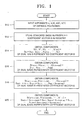
- FIG. 1 is a flowchart of an embodiment of a basis conversion method for converting a standard representation to a dual representation according to the present invention.
- step S10 the exponents n, k(3), k(2), and (k1) of a defining polynomial is input.
- step S12 a coefficient vector B to be subjected to basis conversion is stored.
- steps S14 through S20 the coefficient vector B is converted to a dual basis represented coefficient vector B' .
- the present invention provides basis conversion matrices D sd and D ds and a basis conversion method for a case where a defining polynomial is a pentanomial defined by Formula (31) and satisfies the condition shown in Formula (32).
- a defining polynomial is a pentanomial defined by Formula (31) and satisfies the condition shown in Formula (32).
- the basis conversion matrix D sd is easily expressed linearly with respect to k(t) and "n". This means that a basis conversion matrix does not need to be stored.
- step S10 by inputting the exponents n, k(3), k(2), and k(1) of the defining polynomial which is a pentanomial, the basis conversion matrix D sd is determined based on the above-described theory.
- steps S14 through S20 relate to conversion of a coefficient vector for obtaining the components of a dual basis represented coefficient vector. Conversion formulae used in steps S14 through S20 are determined based on the basis conversion matrix D sd determined in step S10.
- the rows of the basis conversion matrix D sd can be divided into the square matrix [D sd ] U composed of 0-th through k(1)-th rows in a size of (k(1)+1) ⁇ (k(1)+1) and the square matrix [D sd ] L composed of (k(1)+1)-th through (n-1)-th rows in a size of (n-k(1)-1) ⁇ (n-k(1)-1).
- step S14 the 0-th through k(1)-th components [b' 0 , b' 1 , ..., b' k(1) ] T of the dual basis represented coefficient vector B' are obtained using Formula (37).
- [D sd ] U is the same as shown in Formula (34).
- B ' U [D sd ] U ⁇ B U
- steps S16 through S20 the (k(1)+1)-th through (n-1)-th components of the dual basis represented coefficient vector B ' are obtained using Formula (39).
- [D sd ] L is the same as shown in Formula (35).
- the rows in [D sd ] L can be classified into rows having a single 1, rows having two 1s, and rows having three 1s. Accordingly, steps for implementing the right side of conversion Formula (39) can be classified into step S16 having a single term, step S18 having two terms, and step S20 having three terms.
- the 0-th through k(1)-th components of the dual basis represented coefficient vector B' are obtained in step S14, the (k(1)+1)-th through (k(1)+n-k(3))-th components of the dual basis represented coefficient vector B' are obtained in step S16, the (k(1)+1+n-k(3))-th through (k(1)+n-k(2))-th components of the dual basis represented coefficient vector B' are obtained in step S18, and the (k(1)+1+n-k(2))-th through (n-1)-th components of the dual basis represented coefficient vector B' are obtained in step S20. Consequently, the basis conversion result obtained by performing steps S14 through S20 is expressed by Formula (40).
- a basis conversion matrix D sd for converting a standard representation to a dual representation is a 13 ⁇ 13 square matrix expressed by Formula (42).
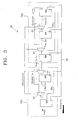
- FIG. 2 is a diagram of an embodiment of an apparatus for basis conversion, by which the basis conversion method shown in FIG. 1 is performed, according to the present invention.
- the apparatus for basis conversion includes a token register 20, which is composed of "n" bits and outputs components of each row of a basis conversion matrix; a token controller 10, which outputs control signals SEL ⁇ 0:n-2>, EN u , and EN l for controlling the token register 20 and data D ⁇ 0:n-1> to the token register 20, the control signal SEL ⁇ 0:n-2> being used for input selection; a data register 30, which is composed of "n” bits and stores the components of a vector to be converted; an AND gate unit 40, which is composed of "n” number of AND gates in order to multiply the n-bit output of the token register 20 by the n-bit output of the data register 30 bit-by-bit; an XOR gate 50, which is connected to the AND gate unit 40 and performs a bit addition on the "n” outputs of the AND gate unit 40; and an output register 60
- the AND gate unit 40, the XOR gate 50, and the output register 60 are illustrated in detail in FIG. 4.
- FIG. 3 is a diagram of an embodiment of the internal structure of the token register 20 shown in FIG. 2.
- the token register 20 includes an upper token register 20a composed of (k(1)+1) bits, a lower token register 20b composed of (n-k(1)-1) bits, and n-1 multiplexers 21, which divide the token register 20 into the upper token register 20a and the lower token register 20b and select data input paths for the token register 20.
- the token register 20 is composed of "n" shift registers, which are classified into the upper token register 20a and the lower token register 20b.
- the token register 20 in response to the enable signals EN u , and EN l and a shift clock CK from the token controller 10, data is shifted to the left by one bit at each shift clock CK and then output.
- the outputs T ⁇ 0:n-1> of the "n" shift registers at each shift clock CK are the values of the components of each row in the basis conversion matrix D sd or D ds .
- the multiplexers 21 divide the token register 20 into the upper token register 20a and the lower token register 20b according to the value of k(1) in response to SEL ⁇ 0:n-2>.
- the token controller 10 receives the exponents n, k(3), k(2), and k(1) of a pentanomial as a defining polynomial and outputs SEL ⁇ 0:n-2> for the (n-1) multiplexers 21, the enable signals EN u , and EN l for activating the shift operation of the token register 20, the shift clock CK for the token register 20, and the data D ⁇ 0:n-1> stored in the upper token register 20a and the lower token register 20b at each shift clock CK.
- Multiplication between a basis conversion matrix and a coefficient vector is implemented by the AND gate unit 40 and the XOR gate 50.
- the AND gate unit 40 performs a bit multiplication of T ⁇ 0:n-1> and D ⁇ 0:n-1>.
- the XOR gate 50 adds the results of the bit multiplication performed by the AND gate unit 40.
- the output register 60 is selectively provided for output synchronization. For example, when the components of each row are determined at 0-th through twelfth clocks, the output register 60 receives the components and outputs vector components at first through thirteenth clocks.
- the 0-th through k(1)-th registers are classified into the upper token register 20a and the (k(1)+1)-th through (n-1)-th registers are classified into the lower token register 20b. Accordingly, the upper and lower token registers 20a and 20b are separately controlled.
- the bit k(1) is the most significant bit (MSB) of the upper token register 20a.
- MSB most significant bit
- the (n-1)-th register corresponding to the MSB of the lower token register 20b is not connected to any one of the multiplexers 21 but always receives external data.
- the upper token register 20a is compose of two shift registers
- the lower token register 20b is compose of 11 shift registers
- 12 multiplexers 21 are provided except for the MSB of the lower token register 20b.
- a value 1 is input to SEL ⁇ 0:k(1)> so that an initial value for the upper token register 20a is externally input.
- the values of SEL ⁇ k(1)+1:n-2> provided for all of the bits of the lower token register 20b except for the (n-1)-th bit are, for example, 1 at the (k(1)+1)-th clock so that the lower token register 20b is connected to external inputs D ⁇ k(1)+1:n-1> at the (k(1)+1)-th clock.
- 0 is input to all of SEL ⁇ k(1)+1:n-2> so that each of registers in the lower token register 20b shifts a value output from the next register.
- the outputs of the upper token register 20a and the lower token register 20b are controlled by the enable signals EN u , and EN l .
- the enable signals EN u , and EN l are controlled to enable the token register 20 while desired values are output in response to the clock CK.
- the following description concerns an example of an enable control of the token register 20.
- the upper token register 20a is enabled at the 0-th clock in response to the enable signal EN u , maintained enabled up to the (k(1)+1)-th clock, and disabled after the shift output of the upper token register 20 at the (k(1)+1)-th clock.
- the upper token register 20a is enabled at the 0-th clock and outputs (1 1) in response to external inputs.
- the upper token register 20a outputs a shifted output 1 as the 0-th bit and outputs 0 as the k(1)-th, i.e., first bit in response to an external input. Consequently, the upper token register 20 outputs (1 0).
- a shifted output 0 is output as the 0-th bit, and 0 is outputs as the first bit in response to an external input so that the upper token register 20a outputs (0 0).
- the upper token register 20a is disabled, and thus the outputs (0 0) are maintained.
- the components of [D sd ] U respectively correspond to bits output from the upper token register 20a.
- all of the outputs of the lower token register 20b are 0 at the 0-th through k(1)-th clocks.
- the lower token register 20b can be designed to be enabled at the (k(1)+1)-th clock.
- all of the registers in the apparatus commence operation, for example, all of the outputs of the lower token register 20b are 0 due to a global reset.
- the lower token register 20b is enabled and starts shift operation.
- the lower token register 20b outputs 0 at the 0-th and first clocks and is enabled at the second clock so as to output (0 0 ... 0 1) in response to external inputs.
- the enabled state is maintained until the basis conversion is completed at the twelfth clock.
- the lower token register 20b outputs (0 0 ... 1 0) by performing a 1-bit shift to the left.
- the 1-bit shift to the left is performed at each clock.
- the upper token register 20a and the lower token register 20b have the following values.
- two bits in a parenthesis are the outputs of the upper token register 20a
- the following 11 bits are the outputs of the lower token register 20b.
- basis conversion matrix calculation is implemented by a bit-by-bit multiplication between the outputs of the token register 20 and the outputs of the data register 40 and an addition of all bits resulting from the bit-by-bit multiplication.
- the components T ⁇ 0:n-1> of each row in the basis conversion matrix D sd which are output from the token register 20 in response to the shift clocks, are respectively multiplied by the values b ⁇ 0:n-1> output from the data register 30 by the "n" AND gates included in the AND gate unit 40.
- the outputs of the AND gate unit 40 are added by the XOR gate 50.
- the output of the XOR gate 50 is synchronized with the clock CK by the output register 60.
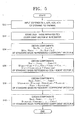
- FIG. 5 is a flowchart of an embodiment of a basis conversion method for converting a dual representation to a standard representation according to the present invention.
- step S30 the exponents n, k(3), k(2), and (k1) of a defining polynomial is input.
- step S32 a coefficient vector B' to be subjected to basis conversion is stored.
- steps S34 through S40 the coefficient vector B' is converted to a standard basis represented coefficient vector B .
- the basis conversion shown in FIG. 5 is similar to that shown in FIG. 1, but a different basis conversion matrix is used.
- the basis conversion matrix D ds for converting a dual representation to a standard representation is an inverse matrix of the basis conversion matrix D sd and expressed by Formulae (45) through (47).
- the number of 1s in each anti-diagonal and an interval between adjacent anti-diagonals are the same as described in the case of the basis conversion matrix D sd .
- steps S36 through S40 the (k(1)+1)-th through (n-1)-th components of the standard basis represented coefficient vector B are obtained using Formula (51).
- [D ds ] L is the same as shown in Formula (47).
- B L [D ds ] L ⁇ B ' L
- the rows in [D ds ] L can be classified into rows having three 1 s, rows having two 1 s, and rows having a single 1. Accordingly, steps for implementing the right side of conversion Formula (50) can be classified into step S36 having three terms, step S38 having two terms, and step S40 having a single term.
- the 0-th through k(1)-th components of the standard basis represented coefficient vector B are obtained in step S34, the (k(1)+1)-th through (k(1)+n-k(3))-th components of the standard basis represented coefficient vector B are obtained in step S36, the (k(1)+1+n-k(3))-th through (k(1)+n-k(2))-th components of the standard basis represented coefficient vector B are obtained in step S38, and the (k(1)+1+n-k(2))-th through (n-1)-th components of the standard basis represented coefficient vector B are obtained in step S40. Consequently, the basis conversion result obtained by performing steps S34 through S40 is expressed by Formula (52).
- An apparatus for basis conversion from a dual representation to a standard representation fundamentally includes the apparatus shown in FIG. 2 and performs the same control and arithmetic operations as the apparatus shown in FIG. 2, with the exception that a data signal D ⁇ 0:n-1> output from the token controller 10 and stored in the upper and lower token registers 20a and 20b is different from that used in the apparatus shown in FIG. 2.
- the upper token register 20a When the defining polynomial is x 13 + x 6 + x 4 + x + 1, in the upper token register 20a corresponding to the components of [D ds ] U , after an initial value is set at the 0-th clock, a value 0 is input as the k(1)-th bit at each clock.
- the upper token register 20a is designed to shift to the left by one bit at each clock.
- the lower token register 20b corresponding to the components of [D ds ] L , after an initial value is set at the (k(1)+1)-th clock, a value 0 is input to the (n-1)-th register at each clock starting from the (k(1)+2)-th clock.
- the lower token register 20b is designed to shift to the left by one bit at each clock.
- the stored initial values are shifted to the left by one bit at each clock.
- a value 0 is input to the 12th register at each clock.
- the upper token register 20a and the lower token register 20b have the following values.
- 0-th clock (0 1) (0 0 0 0 0 0 0 0 0 0 0 0 0 0 0) 1st clock (1 1) (0 0 0 0 0 0 0 0 0 0 0 0 0) 2nd clock (0 0) (0 1 0 1 0 0 0 0 0 1)
- 3rd clock (0 0) (1 0 1 0 0 0 0 0 0 0 1 0)
- 4th clock (0 0) (0 1 0 0 0 0 0 0 0 1 0 0)
- 5th clock (0 0) (1 0 0 0 0 0 0 1 0 0 0 0)
- 6th clock (0 0) (0 0 0 0 0 0 1 0 0 0 0)
- basis conversion matrix calculation is implemented by a bit-by-bit multiplication between the outputs of the token register 20 and the outputs of the data register 40 and an addition of all bits resulting from the bit-by-bit multiplication.
- the components T ⁇ 0:n-1> of each row in the basis conversion matrix D sd which are output from the token register 20 in response to the shift clocks, are respectively multiplied by the values b ⁇ 0:n-1> output from the data register 30 by the "n" AND gates included in the AND gate unit 40.
- the outputs of the AND gate unit 40 are added by the XOR gate 50.
- the output of the XOR gate 50 is output in synchronization with the clock CK by the output register 60.
- a normal pentanomial in an arbitrary degree is used as a defining polynomial so that basis conversion between a standard representation and a dual representation is efficiently performed. Consequently, a dual basis multiplier can be efficiently implemented.
- Finite field multiplication is one of the factors controlling performance and required processing power. For example, within an elliptic curve cryptosystem the signature time will depend on the multiplication efficiency. Multiplication using a Dual basis is efficient in terms of the algorithm used.
- Figure 6 shows a multiplication apparatus according to the invention.
- the apparatus comprises a basis conversion unit 100 for conversion from the standard basis to the dual basis, and which is in accordance with the invention.
- a dual basis multiplier 102 performs dual basis multiplication, and is known the in art.
- a further basis conversion unit 104 is for conversion from the dual basis back to the standard basis.
- the apparatus of Figure 6 can be used in Reed-Solomon systems, in cryptosystems, for example elliptic curve cryptosystems, in error correction systems and in other computationally intense applications.
Landscapes
- Physics & Mathematics (AREA)
- Engineering & Computer Science (AREA)
- General Physics & Mathematics (AREA)
- Mathematical Analysis (AREA)
- Mathematical Optimization (AREA)
- Pure & Applied Mathematics (AREA)
- Computational Mathematics (AREA)
- Theoretical Computer Science (AREA)
- Computing Systems (AREA)
- General Engineering & Computer Science (AREA)
- Mathematical Physics (AREA)
- Error Detection And Correction (AREA)
- Complex Calculations (AREA)
Applications Claiming Priority (2)
| Application Number | Priority Date | Filing Date | Title |
|---|---|---|---|
| KR2002069460 | 2002-11-09 | ||
| KR10-2002-0069460A KR100486726B1 (ko) | 2002-11-09 | 2002-11-09 | 유한 체에서의 기저 변환 방법 및 기저 변환 장치 |
Publications (3)
| Publication Number | Publication Date |
|---|---|
| EP1455270A2 true EP1455270A2 (de) | 2004-09-08 |
| EP1455270A3 EP1455270A3 (de) | 2006-06-28 |
| EP1455270B1 EP1455270B1 (de) | 2007-03-28 |
Family
ID=32291720
Family Applications (1)
| Application Number | Title | Priority Date | Filing Date |
|---|---|---|---|
| EP03257026A Expired - Lifetime EP1455270B1 (de) | 2002-11-09 | 2003-11-06 | Vorrichtung und Verfahren zur Basiskonvertierung in endliche Körper und einen Multiplizierer |
Country Status (6)
| Country | Link |
|---|---|
| US (1) | US7346641B2 (de) |
| EP (1) | EP1455270B1 (de) |
| JP (1) | JP3823107B2 (de) |
| KR (1) | KR100486726B1 (de) |
| CN (1) | CN1313918C (de) |
| DE (1) | DE60312810T2 (de) |
Families Citing this family (7)
| Publication number | Priority date | Publication date | Assignee | Title |
|---|---|---|---|---|
| KR100871221B1 (ko) * | 2005-11-11 | 2008-12-01 | 삼성전자주식회사 | 선형 궤환 시프트 레지스터를 이용하는 통신 시스템에서부호 생성 방법 및 장치 |
| CN101008937B (zh) * | 2007-02-06 | 2010-05-19 | 中国科学院研究生院 | 提高有限域上乘法以及大矩阵消元的计算速度的方法 |
| US8380777B2 (en) * | 2007-06-30 | 2013-02-19 | Intel Corporation | Normal-basis to canonical-basis transformation for binary galois-fields GF(2m) |
| US8380767B2 (en) * | 2007-06-30 | 2013-02-19 | Intel Corporation | Polynomial-basis to normal-basis transformation for binary Galois-Fields GF(2m) |
| US8176395B2 (en) * | 2007-11-27 | 2012-05-08 | Macronix International Co., Ltd. | Memory module and writing and reading method thereof |
| CN102929574A (zh) * | 2012-10-18 | 2013-02-13 | 复旦大学 | Gf(2163)域上的脉动乘法器设计方法 |
| CN103441813B (zh) * | 2013-08-27 | 2015-11-11 | 湖北大学 | 一种用于cdma系统的低相关二元序列集生成方法 |
Family Cites Families (9)
| Publication number | Priority date | Publication date | Assignee | Title |
|---|---|---|---|---|
| US4994995A (en) * | 1990-03-14 | 1991-02-19 | International Business Machines Corporation | Bit-serial division method and apparatus |
| KR940001147B1 (ko) * | 1991-03-20 | 1994-02-14 | 삼성전자 주식회사 | 부분체 GF(2^m/2)을 이용한 GF(2^m)상의 연산방법 및 장치 |
| US5854759A (en) * | 1997-05-05 | 1998-12-29 | Rsa Data Security, Inc. | Methods and apparatus for efficient finite field basis conversion |
| US6286022B1 (en) | 1997-11-18 | 2001-09-04 | Rsa Security Inc. | Efficient finite field basis conversion involving a dual basis |
| US6389442B1 (en) * | 1997-12-30 | 2002-05-14 | Rsa Security Inc. | Efficient finite field multiplication in normal basis |
| KR100322739B1 (ko) * | 1998-10-19 | 2002-06-22 | 윤종용 | 유한체연산방법및그장치 |
| US6343305B1 (en) * | 1999-09-14 | 2002-01-29 | The State Of Oregon Acting By And Through The State Board Of Higher Education On Behalf Of Oregon State University | Methods and apparatus for multiplication in a galois field GF (2m), encoders and decoders using same |
| US7724898B2 (en) * | 2002-10-17 | 2010-05-25 | Telefonaktiebolaget L M Ericsson (Publ) | Cryptography using finite fields of odd characteristic on binary hardware |
| US7197527B2 (en) * | 2002-10-17 | 2007-03-27 | Telefonaktiebolaget Lm Ericsson (Publ) | Efficient arithmetic in finite fields of odd characteristic on binary hardware |
-
2002
- 2002-11-09 KR KR10-2002-0069460A patent/KR100486726B1/ko not_active Expired - Fee Related
-
2003
- 2003-07-25 CN CNB031436145A patent/CN1313918C/zh not_active Expired - Fee Related
- 2003-11-06 DE DE60312810T patent/DE60312810T2/de not_active Expired - Fee Related
- 2003-11-06 EP EP03257026A patent/EP1455270B1/de not_active Expired - Lifetime
- 2003-11-07 US US10/702,740 patent/US7346641B2/en not_active Expired - Fee Related
- 2003-11-07 JP JP2003379095A patent/JP3823107B2/ja not_active Expired - Fee Related
Non-Patent Citations (6)
| Title |
|---|
| BERLEKAMP E R: "BIT-SERIAL REED-SOLOMON ENCODERS" IEEE TRANSACTIONS ON INFORMATION THEORY, IEEE SERVICE CENTER, PISCATAWAY, NJ, US, vol. 28, no. 6, 1 November 1982 (1982-11-01), pages 869-874, XP000575333 ISSN: 0018-9448 * |
| DIETER GOLLMANN: "Equally Spaced Polynomials, Dual Bases, and Multiplication in F2^n" IEEE TRANSACTIONS ON COMPUTERS, vol. 51, no. 5, May 2002 (2002-05), pages 588-591, XP009066733 * |
| HASAN M A ET AL: "DIVISION AND BIT-SERIAL MULTIPLICATION OVER GF(QM)" IEE PROCEEDINGS E. COMPUTERS & DIGITAL TECHNIQUES, INSTITUTION OF ELECTRICAL ENGINEERS. STEVENAGE, GB, vol. 139, no. 3, PART E, 1 May 1992 (1992-05-01), pages 230-236, XP000306407 ISSN: 0143-7062 * |
| HSU I S ET AL: "A COMPARISON OF VLSI ARCHITECTURE OF FINITE FIELD MULTIPLIERS USING DUAL, NORMAL, OR STANDARD BASES" IEEE TRANSACTIONS ON COMPUTERS, IEEE SERVICE CENTER, LOS ALAMITOS, CA, US, vol. 37, no. 6, 1 June 1988 (1988-06-01), pages 735-739, XP000576196 ISSN: 0018-9340 * |
| KWON S ET AL: "EFFICIENT BIT SERIAL MULTIPLICATION USING OPTIMAL NORMAL BASES OF TYPE II IN GF(2M)" INFORMATION SECURITY. INTERNATIONAL CONFERENCE: PROCEEDINGS ISC, 30 September 2002 (2002-09-30), pages 300-308, XP001160560 * |
| MASAKATU MORII, MASAO KASAHARA, DOUGLAS L. WHITING: "Efficient Bit-Serial Multiplication and the Discrete-Time Wiener-Hopf Equation Over Finite Fields" IEEE TRANSACTIONS ON INFORMATION THEORY, vol. 35, no. 6, November 1989 (1989-11), pages 1177-1183, XP007900627 * |
Also Published As
| Publication number | Publication date |
|---|---|
| CN1499358A (zh) | 2004-05-26 |
| US7346641B2 (en) | 2008-03-18 |
| DE60312810D1 (de) | 2007-05-10 |
| JP3823107B2 (ja) | 2006-09-20 |
| US20040098437A1 (en) | 2004-05-20 |
| EP1455270A3 (de) | 2006-06-28 |
| KR100486726B1 (ko) | 2005-05-03 |
| DE60312810T2 (de) | 2007-12-06 |
| EP1455270B1 (de) | 2007-03-28 |
| JP2004166274A (ja) | 2004-06-10 |
| CN1313918C (zh) | 2007-05-02 |
| KR20040041282A (ko) | 2004-05-17 |
Similar Documents
| Publication | Publication Date | Title |
|---|---|---|
| Daly et al. | An FPGA implementation of a GF (p) ALU for encryption processors | |
| KR100591761B1 (ko) | 몽고메리 모듈러 곱셈기 및 캐리 저장 가산을 이용한몽고메리 모듈러 곱셈 방법 | |
| JP2004326112A (ja) | マルチプルモジュラス選択器、累算器、モンゴメリー掛け算器、マルチプルモジュラス発生方法、部分掛け発生方法、累算方法、掛け算方法、モジュラス選択器、およびブースレコーダ | |
| CN106484366A (zh) | 一种二元域位宽可变模乘运算器 | |
| JP4180024B2 (ja) | 乗算剰余演算器及び情報処理装置 | |
| US7046800B1 (en) | Scalable methods and apparatus for Montgomery multiplication | |
| Großschädl | A bit-serial unified multiplier architecture for finite fields GF (p) and GF (2m) | |
| EP1455270B1 (de) | Vorrichtung und Verfahren zur Basiskonvertierung in endliche Körper und einen Multiplizierer | |
| Reyhani-Masoleh | A new bit-serial architecture for field multiplication using polynomial bases | |
| JP4170267B2 (ja) | 乗算剰余演算器及び情報処理装置 | |
| KR100322739B1 (ko) | 유한체연산방법및그장치 | |
| Lee | Low-latency bit-parallel systolic multiplier for irreducible x m+ x n+ 1 with gcd (m, n)= 1 | |
| KR100478974B1 (ko) | 직렬 유한체 승산기 | |
| Chen et al. | Scalable and systolic Montgomery multipliers over GF (2 m) | |
| US7607165B2 (en) | Method and apparatus for multiplication and/or modular reduction processing | |
| Chen et al. | Scalable and systolic dual basis multiplier over GF (2m) | |
| EP1600852A2 (de) | Verfahren und Vorrichtung zur Berechnung einer modularen Inversen | |
| WO2003096182A1 (en) | “emod” a fast modulus calculation for computer systems | |
| KR100946256B1 (ko) | 다정도 캐리 세이브 가산기를 이용한 듀얼필드상의확장성있는 몽고매리 곱셈기 | |
| JP3904421B2 (ja) | 剰余乗算演算装置 | |
| US6138134A (en) | Computational method and apparatus for finite field multiplication | |
| JP3210420B2 (ja) | 整数上の乗算回路 | |
| JP3129525B2 (ja) | 整数上の乗算回路 | |
| Rodriguez-Flores et al. | A compact FPGA-based microcoded coprocessor for exponentiation in asymmetric encryption | |
| US7471789B2 (en) | Encryption circuit achieving higher operation speed |
Legal Events
| Date | Code | Title | Description |
|---|---|---|---|
| PUAI | Public reference made under article 153(3) epc to a published international application that has entered the european phase |
Free format text: ORIGINAL CODE: 0009012 |
|
| 17P | Request for examination filed |
Effective date: 20031119 |
|
| AK | Designated contracting states |
Kind code of ref document: A2 Designated state(s): AT BE BG CH CY CZ DE DK EE ES FI FR GB GR HU IE IT LI LU MC NL PT RO SE SI SK TR |
|
| AX | Request for extension of the european patent |
Extension state: AL LT LV MK |
|
| PUAL | Search report despatched |
Free format text: ORIGINAL CODE: 0009013 |
|
| AK | Designated contracting states |
Kind code of ref document: A3 Designated state(s): AT BE BG CH CY CZ DE DK EE ES FI FR GB GR HU IE IT LI LU MC NL PT RO SE SI SK TR |
|
| AX | Request for extension of the european patent |
Extension state: AL LT LV MK |
|
| GRAP | Despatch of communication of intention to grant a patent |
Free format text: ORIGINAL CODE: EPIDOSNIGR1 |
|
| GRAS | Grant fee paid |
Free format text: ORIGINAL CODE: EPIDOSNIGR3 |
|
| GRAA | (expected) grant |
Free format text: ORIGINAL CODE: 0009210 |
|
| AKX | Designation fees paid |
Designated state(s): DE FI FR GB SE |
|
| AK | Designated contracting states |
Kind code of ref document: B1 Designated state(s): DE FI FR GB SE |
|
| REG | Reference to a national code |
Ref country code: GB Ref legal event code: FG4D |
|
| RIN1 | Information on inventor provided before grant (corrected) |
Inventor name: JIN, WEON-IL526-1903 BAEKSEOL MAEUL JINRO APT. Inventor name: HUH, MI-SUK Inventor name: SEO, CHANG-WOO241-1402 HWANGGOL MAEUL SSANGYONG |
|
| REF | Corresponds to: |
Ref document number: 60312810 Country of ref document: DE Date of ref document: 20070510 Kind code of ref document: P |
|
| REG | Reference to a national code |
Ref country code: SE Ref legal event code: TRGR |
|
| PLBE | No opposition filed within time limit |
Free format text: ORIGINAL CODE: 0009261 |
|
| STAA | Information on the status of an ep patent application or granted ep patent |
Free format text: STATUS: NO OPPOSITION FILED WITHIN TIME LIMIT |
|
| 26N | No opposition filed |
Effective date: 20080102 |
|
| PGFP | Annual fee paid to national office [announced via postgrant information from national office to epo] |
Ref country code: DE Payment date: 20081103 Year of fee payment: 6 |
|
| PGFP | Annual fee paid to national office [announced via postgrant information from national office to epo] |
Ref country code: FI Payment date: 20081112 Year of fee payment: 6 |
|
| PGFP | Annual fee paid to national office [announced via postgrant information from national office to epo] |
Ref country code: SE Payment date: 20081107 Year of fee payment: 6 |
|
| PGFP | Annual fee paid to national office [announced via postgrant information from national office to epo] |
Ref country code: FR Payment date: 20081112 Year of fee payment: 6 |
|
| PGFP | Annual fee paid to national office [announced via postgrant information from national office to epo] |
Ref country code: GB Payment date: 20081105 Year of fee payment: 6 |
|
| EUG | Se: european patent has lapsed | ||
| GBPC | Gb: european patent ceased through non-payment of renewal fee |
Effective date: 20091106 |
|
| REG | Reference to a national code |
Ref country code: FR Ref legal event code: ST Effective date: 20100730 |
|
| PG25 | Lapsed in a contracting state [announced via postgrant information from national office to epo] |
Ref country code: FI Free format text: LAPSE BECAUSE OF NON-PAYMENT OF DUE FEES Effective date: 20091106 |
|
| PG25 | Lapsed in a contracting state [announced via postgrant information from national office to epo] |
Ref country code: FR Free format text: LAPSE BECAUSE OF NON-PAYMENT OF DUE FEES Effective date: 20091130 |
|
| PG25 | Lapsed in a contracting state [announced via postgrant information from national office to epo] |
Ref country code: DE Free format text: LAPSE BECAUSE OF NON-PAYMENT OF DUE FEES Effective date: 20100601 |
|
| PG25 | Lapsed in a contracting state [announced via postgrant information from national office to epo] |
Ref country code: GB Free format text: LAPSE BECAUSE OF NON-PAYMENT OF DUE FEES Effective date: 20091106 |
|
| PG25 | Lapsed in a contracting state [announced via postgrant information from national office to epo] |
Ref country code: SE Free format text: LAPSE BECAUSE OF NON-PAYMENT OF DUE FEES Effective date: 20091107 |