EP1455563A1 - Materiau transmettant la lumiere et protege contre les ondes electromagnetiques et procede de fabrication de ce materiau - Google Patents
Materiau transmettant la lumiere et protege contre les ondes electromagnetiques et procede de fabrication de ce materiau Download PDFInfo
- Publication number
- EP1455563A1 EP1455563A1 EP02803497A EP02803497A EP1455563A1 EP 1455563 A1 EP1455563 A1 EP 1455563A1 EP 02803497 A EP02803497 A EP 02803497A EP 02803497 A EP02803497 A EP 02803497A EP 1455563 A1 EP1455563 A1 EP 1455563A1
- Authority
- EP
- European Patent Office
- Prior art keywords
- electromagnetic
- light transmitting
- wave shielding
- pattern
- transmitting plate
- Prior art date
- Legal status (The legal status is an assumption and is not a legal conclusion. Google has not performed a legal analysis and makes no representation as to the accuracy of the status listed.)
- Granted
Links
- 238000004519 manufacturing process Methods 0.000 title claims abstract description 15
- 239000000463 material Substances 0.000 title description 8
- 229920005989 resin Polymers 0.000 claims abstract description 36
- 239000011347 resin Substances 0.000 claims abstract description 36
- 239000004020 conductor Substances 0.000 claims abstract description 12
- 238000007747 plating Methods 0.000 claims description 11
- 238000000034 method Methods 0.000 claims description 8
- PXHVJJICTQNCMI-UHFFFAOYSA-N Nickel Chemical compound [Ni] PXHVJJICTQNCMI-UHFFFAOYSA-N 0.000 claims description 6
- 229920000122 acrylonitrile butadiene styrene Polymers 0.000 claims description 6
- 238000007639 printing Methods 0.000 claims description 6
- RYGMFSIKBFXOCR-UHFFFAOYSA-N Copper Chemical compound [Cu] RYGMFSIKBFXOCR-UHFFFAOYSA-N 0.000 claims description 5
- 229910052802 copper Inorganic materials 0.000 claims description 5
- 239000010949 copper Substances 0.000 claims description 5
- VYZAMTAEIAYCRO-UHFFFAOYSA-N Chromium Chemical compound [Cr] VYZAMTAEIAYCRO-UHFFFAOYSA-N 0.000 claims description 3
- BQCADISMDOOEFD-UHFFFAOYSA-N Silver Chemical compound [Ag] BQCADISMDOOEFD-UHFFFAOYSA-N 0.000 claims description 3
- ATJFFYVFTNAWJD-UHFFFAOYSA-N Tin Chemical compound [Sn] ATJFFYVFTNAWJD-UHFFFAOYSA-N 0.000 claims description 3
- HCHKCACWOHOZIP-UHFFFAOYSA-N Zinc Chemical compound [Zn] HCHKCACWOHOZIP-UHFFFAOYSA-N 0.000 claims description 3
- 230000015572 biosynthetic process Effects 0.000 claims description 3
- 229910052804 chromium Inorganic materials 0.000 claims description 3
- 239000011651 chromium Substances 0.000 claims description 3
- PCHJSUWPFVWCPO-UHFFFAOYSA-N gold Chemical compound [Au] PCHJSUWPFVWCPO-UHFFFAOYSA-N 0.000 claims description 3
- 229910052737 gold Inorganic materials 0.000 claims description 3
- 239000010931 gold Substances 0.000 claims description 3
- 229910052759 nickel Inorganic materials 0.000 claims description 3
- 229910052709 silver Inorganic materials 0.000 claims description 3
- 239000004332 silver Substances 0.000 claims description 3
- 229910052718 tin Inorganic materials 0.000 claims description 3
- 229910052725 zinc Inorganic materials 0.000 claims description 3
- 239000011701 zinc Substances 0.000 claims description 3
- 229920002284 Cellulose triacetate Polymers 0.000 claims description 2
- 229920000089 Cyclic olefin copolymer Polymers 0.000 claims description 2
- 229930182556 Polyacetal Natural products 0.000 claims description 2
- NNLVGZFZQQXQNW-ADJNRHBOSA-N [(2r,3r,4s,5r,6s)-4,5-diacetyloxy-3-[(2s,3r,4s,5r,6r)-3,4,5-triacetyloxy-6-(acetyloxymethyl)oxan-2-yl]oxy-6-[(2r,3r,4s,5r,6s)-4,5,6-triacetyloxy-2-(acetyloxymethyl)oxan-3-yl]oxyoxan-2-yl]methyl acetate Chemical compound O([C@@H]1O[C@@H]([C@H]([C@H](OC(C)=O)[C@H]1OC(C)=O)O[C@H]1[C@@H]([C@@H](OC(C)=O)[C@H](OC(C)=O)[C@@H](COC(C)=O)O1)OC(C)=O)COC(=O)C)[C@@H]1[C@@H](COC(C)=O)O[C@@H](OC(C)=O)[C@H](OC(C)=O)[C@H]1OC(C)=O NNLVGZFZQQXQNW-ADJNRHBOSA-N 0.000 claims description 2
- 229920000058 polyacrylate Polymers 0.000 claims description 2
- 229920006324 polyoxymethylene Polymers 0.000 claims description 2
- 239000011135 tin Substances 0.000 claims description 2
- 238000007772 electroless plating Methods 0.000 abstract description 4
- 239000000758 substrate Substances 0.000 description 4
- ZWEHNKRNPOVVGH-UHFFFAOYSA-N 2-Butanone Chemical compound CCC(C)=O ZWEHNKRNPOVVGH-UHFFFAOYSA-N 0.000 description 3
- 239000002253 acid Substances 0.000 description 3
- 229920002120 photoresistant polymer Polymers 0.000 description 3
- 239000004721 Polyphenylene oxide Substances 0.000 description 2
- QAOWNCQODCNURD-UHFFFAOYSA-N Sulfuric acid Chemical compound OS(O)(=O)=O QAOWNCQODCNURD-UHFFFAOYSA-N 0.000 description 2
- 229910045601 alloy Inorganic materials 0.000 description 2
- 239000000956 alloy Substances 0.000 description 2
- 238000007646 gravure printing Methods 0.000 description 2
- 229910052751 metal Inorganic materials 0.000 description 2
- 239000002184 metal Substances 0.000 description 2
- 230000003647 oxidation Effects 0.000 description 2
- 238000007254 oxidation reaction Methods 0.000 description 2
- BASFCYQUMIYNBI-UHFFFAOYSA-N platinum Chemical compound [Pt] BASFCYQUMIYNBI-UHFFFAOYSA-N 0.000 description 2
- 239000004417 polycarbonate Substances 0.000 description 2
- 229920006289 polycarbonate film Polymers 0.000 description 2
- 229920006380 polyphenylene oxide Polymers 0.000 description 2
- 229920003002 synthetic resin Polymers 0.000 description 2
- 239000000057 synthetic resin Substances 0.000 description 2
- 229910000599 Cr alloy Inorganic materials 0.000 description 1
- 229920000297 Rayon Polymers 0.000 description 1
- RTAQQCXQSZGOHL-UHFFFAOYSA-N Titanium Chemical compound [Ti] RTAQQCXQSZGOHL-UHFFFAOYSA-N 0.000 description 1
- NIXOWILDQLNWCW-UHFFFAOYSA-N acrylic acid group Chemical group C(C=C)(=O)O NIXOWILDQLNWCW-UHFFFAOYSA-N 0.000 description 1
- 229910052782 aluminium Inorganic materials 0.000 description 1
- XAGFODPZIPBFFR-UHFFFAOYSA-N aluminium Chemical compound [Al] XAGFODPZIPBFFR-UHFFFAOYSA-N 0.000 description 1
- 230000005540 biological transmission Effects 0.000 description 1
- 229910052793 cadmium Inorganic materials 0.000 description 1
- BDOSMKKIYDKNTQ-UHFFFAOYSA-N cadmium atom Chemical compound [Cd] BDOSMKKIYDKNTQ-UHFFFAOYSA-N 0.000 description 1
- 230000001413 cellular effect Effects 0.000 description 1
- KRVSOGSZCMJSLX-UHFFFAOYSA-L chromic acid Substances O[Cr](O)(=O)=O KRVSOGSZCMJSLX-UHFFFAOYSA-L 0.000 description 1
- 239000000788 chromium alloy Substances 0.000 description 1
- 229910017052 cobalt Inorganic materials 0.000 description 1
- 239000010941 cobalt Substances 0.000 description 1
- GUTLYIVDDKVIGB-UHFFFAOYSA-N cobalt atom Chemical compound [Co] GUTLYIVDDKVIGB-UHFFFAOYSA-N 0.000 description 1
- AWJWCTOOIBYHON-UHFFFAOYSA-N furo[3,4-b]pyrazine-5,7-dione Chemical compound C1=CN=C2C(=O)OC(=O)C2=N1 AWJWCTOOIBYHON-UHFFFAOYSA-N 0.000 description 1
- 229910052738 indium Inorganic materials 0.000 description 1
- APFVFJFRJDLVQX-UHFFFAOYSA-N indium atom Chemical compound [In] APFVFJFRJDLVQX-UHFFFAOYSA-N 0.000 description 1
- 238000007641 inkjet printing Methods 0.000 description 1
- 150000002739 metals Chemical class 0.000 description 1
- 239000000203 mixture Substances 0.000 description 1
- 229910052697 platinum Inorganic materials 0.000 description 1
- 229920000515 polycarbonate Polymers 0.000 description 1
- 238000007650 screen-printing Methods 0.000 description 1
- 239000000126 substance Substances 0.000 description 1
- 239000010936 titanium Substances 0.000 description 1
- 229910052719 titanium Inorganic materials 0.000 description 1
- 238000002834 transmittance Methods 0.000 description 1
- 229910052720 vanadium Inorganic materials 0.000 description 1
- LEONUFNNVUYDNQ-UHFFFAOYSA-N vanadium atom Chemical compound [V] LEONUFNNVUYDNQ-UHFFFAOYSA-N 0.000 description 1
Images
Classifications
-
- H—ELECTRICITY
- H05—ELECTRIC TECHNIQUES NOT OTHERWISE PROVIDED FOR
- H05K—PRINTED CIRCUITS; CASINGS OR CONSTRUCTIONAL DETAILS OF ELECTRIC APPARATUS; MANUFACTURE OF ASSEMBLAGES OF ELECTRICAL COMPONENTS
- H05K9/00—Screening of apparatus or components against electric or magnetic fields
- H05K9/0073—Shielding materials
- H05K9/0094—Shielding materials being light-transmitting, e.g. transparent, translucent
- H05K9/0096—Shielding materials being light-transmitting, e.g. transparent, translucent for television displays, e.g. plasma display panel
-
- H—ELECTRICITY
- H05—ELECTRIC TECHNIQUES NOT OTHERWISE PROVIDED FOR
- H05K—PRINTED CIRCUITS; CASINGS OR CONSTRUCTIONAL DETAILS OF ELECTRIC APPARATUS; MANUFACTURE OF ASSEMBLAGES OF ELECTRICAL COMPONENTS
- H05K3/00—Apparatus or processes for manufacturing printed circuits
- H05K3/10—Apparatus or processes for manufacturing printed circuits in which conductive material is applied to the insulating support in such a manner as to form the desired conductive pattern
- H05K3/18—Apparatus or processes for manufacturing printed circuits in which conductive material is applied to the insulating support in such a manner as to form the desired conductive pattern using precipitation techniques to apply the conductive material
- H05K3/181—Apparatus or processes for manufacturing printed circuits in which conductive material is applied to the insulating support in such a manner as to form the desired conductive pattern using precipitation techniques to apply the conductive material by electroless plating
- H05K3/182—Apparatus or processes for manufacturing printed circuits in which conductive material is applied to the insulating support in such a manner as to form the desired conductive pattern using precipitation techniques to apply the conductive material by electroless plating characterised by the patterning method
-
- H—ELECTRICITY
- H05—ELECTRIC TECHNIQUES NOT OTHERWISE PROVIDED FOR
- H05K—PRINTED CIRCUITS; CASINGS OR CONSTRUCTIONAL DETAILS OF ELECTRIC APPARATUS; MANUFACTURE OF ASSEMBLAGES OF ELECTRICAL COMPONENTS
- H05K2203/00—Indexing scheme relating to apparatus or processes for manufacturing printed circuits covered by H05K3/00
- H05K2203/05—Patterning and lithography; Masks; Details of resist
- H05K2203/0502—Patterning and lithography
- H05K2203/0522—Using an adhesive pattern
Definitions
- the present invention relates to an electromagnetic-wave shielding and light transmitting plate which can be suitably used as a front filter for a PDP (plasma display panel) or a window sheet (for example, a bonding film) for a building such as a hospital where needs electromagnetic-wave shielding and to a manufacturing method of the same. More particularly, the present invention relates to an electromagnetic-wave shielding and light transmitting plate which comprises a film and a conductive pattern formed on the film and to a manufacturing method of the same.
- Plates having electromagnetic-wave shielding property and light transmission properties have been developed as front filters of equipment such as office automation equipment and communication equipment in order to shield electromagnetic wave produced from such equipment.
- Such plates have been also utilized as window sheets of places where a precision apparatus is installed, such as a hospital and a laboratory, in order to protect the precision apparatus from electromagnetic waves for example from cellular phones.
- a conventional electromagnetic-wave shielding and light transmitting plate typically comprises a pair of transparent substrates such as acrylic boards and a conductive mesh member like a wire netting or a transparent conductive film and is formed by interposing the conductive mesh member or the transparent conductive film between the transparent substrates and uniting them.
- a conductive mesh member employed in the conventional electromagnetic-wave shielding and light transmitting plate is a 5- to 500-mesh member having a wire diameter of from 10 to 500 ⁇ m and an open area ratio (open area percentage) of less than 75 %.
- the open area ratio is calculated from the wire diameter of mesh and the number of wires existing within a width of 1 inch.
- the electromagnetic-wave shielding and light transmitting plate employing such a conductive mesh member has low light transmittance of 70 % at the most.
- such a conventional conductive mesh member easily allows the occurrence of moiré phenomenon due to relations between its patterns and the pixel pitch of a luminescent panel to which the electromagnetic-wave shielding and light transmitting plate is attached.
- the conductive mesh member In case of the conductive mesh member, by designing the conductive mesh member to have margins out of the peripheries of the transparent substrate and folding the margins, the electric conduction between the folded margins and the panel body is achieved. If the transparent conductive film is designed to have margins out of the transparent substrate and the margins are folded, the film may be torn at the folded portions.
- a method of manufacturing an electromagnetic-wave shielding and light transmitting plate according to the present invention is a method for manufacturing an electromagnetic-wave shielding and light transmitting plate comprising a transparent film and a conductive pattern made of a conductive material, wherein the conductive pattern is formed on a surface of the transparent film by plating.
- the method comprises: a step of forming a resin pattern to be the same pattern as the conductive pattern, wherein the resin pattern is formed on the surface of the transparent film having a relatively low affinity for the plated layer by using a resin having a relatively high affinity for the plated layer, and a step of forming the conductive pattern by subjecting the transparent film to plating treatment with plating solution after the formation of the resin pattern so as to attach the conductive material only to the resin pattern.
- An electromagnetic-waveshielding andlight transmitting plate of the present invention comprises a transparent film having a relatively low affinity for a plated layer, a resin pattern formed on a surface of the transparent film and having a relatively high affinity for the plated layer, and a conductive pattern composed of the plated layer of a conductive material which is formed on the resin pattern.
- the resin for forming the resin pattern has low viscosity.
- the conductive pattern formed on the resin pattern has a significantly narrow line width and thus has a significantly large open area ratio.
- an electromagnetic-wave shielding and light transmitting plate having a conductive pattern of which line width is 200 ⁇ m or less and open area ratio is 75% or more can be manufactured.
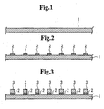
- Figs. 1, 2, and 3 are sectional views showing an embodiment of the method according to the present invention.
- a resin pattern 2 is printed in a grid configuration by using a resin material having a relatively high affinity for a plated layer of a conductive material on a transparent film 1 having a relatively low affinity for the plated layer. Then, the transparent film 1 is subjected to plating treatment so as to form a conductive pattern 3 as a plated layer of a conductive material only on the resin pattern 2 as shown in Fig. 3.
- the conductive pattern 3 Since the conductive pattern 3 is formed on the resin pattern 2 in the grid configuration, the conductive pattern 3 has the same grid configuration as that of the resin pattern 2. By setting the line width of the resin pattern 2 narrower, the conductive pattern 3 having a grid configuration of a narrower line width is obtained. By setting the line width of the resin pattern 2 having a grid configuration to be narrower and designing the resin pattern 2 to have larger open area, the conductive pattern 3 having a grid configuration of a larger open area ratio is obtained.
- a transparent synthetic resin having a low affinity for the plated layer of the conductive material is employed.
- the synthetic resin include PC (polycarbonate), cycloolefin polymer, polyallylate, and acrylic polymer.
- a transparent film made of material having a low affinity for the plated layer as its chemical property is preferably used and a transparent film of which surface is not etched and affinity for the plated layer never be intensified even when it is in contact with plating solution is more preferably used.
- the thickness of the transparent film depends on the application of the electromagnetic-wave shielding and light transmitting plate and usually is in a range of from 1 ⁇ m to 5 mm.
- the resin pattern 2 on the film 1 is preferably formed byprinting.
- the printing material are materials commercially-designated as photoresist. Among such materials, solution of ABS, triacetylcellulose, polyacetal, or modified PPO (polyphenylene oxide) is suitable.
- the printed photoresist is hardened by irradiation of energy beam such as ultraviolet ray and is then subjected to plating treatment.
- the resin pattern 2 is printed to be a grid configuration.
- the line width of this pattern is preferably 200 ⁇ m or less, more preferably 100 ⁇ m or less, especially preferably 30 ⁇ m or less.
- the printing method gravure printing, screen printing, ink jet printing, or electrostatic printing can be suitably employed. In order to minimize the line width, the gravure printing is suitable.
- the printing thickness of the resin pattern is not particularly limited and usually is in a range of from 0.1 ⁇ m to 10 ⁇ m.
- Examples suitably used as the conductive material forming the conductive pattern 3 are metals of aluminum, nickel, indium, chromium, gold, vanadium, tin, cadmium, silver, platinum, copper, titanium, cobalt, and zinc and alloys thereof. Among these, puremetals of copper, nickel, chromium, zinc, tin, silver, and gold and alloys thereof are preferable.
- the thickness of the conductive pattern 3 is preferably from 0.1 ⁇ m to 10 ⁇ m. When the thickness is less than 0.1 ⁇ m, the electromagnetic-wave shielding property must be insufficient. When the thickness of the pattern 3 is larger than 10 ⁇ m, the view angle of the electromagnetic-wave shilding and light transmitting plate may be narrow and the plating may spread in the width direction so as to increase the line width, thus reducing the open area ratio.
- electroless plating is preferable.
- the resin pattern 2 Before the electroless plating, the resin pattern 2 may be subjected to pretreatment with acid.
- the pretreatment with acid increases the affinity for the plated layer of the resin pattern 2.
- the acid include chromic acid, sulfuric acid, and blend thereof.
- blackening treatment maybe applied in order to impart antidazzle property.
- oxidation treatment of metal or black plating treatment with chromium alloy may be employed.
- the electromagnetic-wave shielding and light transmitting plate manufactured as mentioned above may be a piece of film or a continuous web-like film which is accommodated in a roll form.
- a grid was printed on a polycarbonate film of 100 ⁇ m in thickness by using 20% solution in which ABS resin (3001M available from Mitsubishi Rayon Co., Ltd.) was dissolved in methyl ethyl ketone.
- the ABS resin pattern was regularly aligned in a square grid configuration so that the line width of the grid was 20 ⁇ m, one side of each aperture of the grid was 250 ⁇ m, and the open area ratio was 80%.
- the printing thickness after dried is 2 ⁇ m.
- Copper was plated on the grid of ABS resin pattern by means of the electroless plating in such a manner as to have an average thickness of 2 ⁇ m. Finally, blackening treatment was applied by means of oxidation treatment, thereby obtaining an electromagnetic-wave shielding and light transmitting plate. It should be noted that the copper is not attached to the surface of the polycarbonate film at all.
- the conductive pattern on the surface of the film was regularly aligned in a square grid configuration so that the line width was 20 ⁇ m, one side of each aperture of the grid was 250 ⁇ m, and the open area ratio was 80% just like the ABS resin pattern.
- an electromagnetic-wave shielding and light transmitting plate having a conductive pattern of which line width is narrow and open area ratio is high can be manufactured.
Landscapes
- Engineering & Computer Science (AREA)
- Microelectronics & Electronic Packaging (AREA)
- Manufacturing & Machinery (AREA)
- Physics & Mathematics (AREA)
- Plasma & Fusion (AREA)
- Shielding Devices Or Components To Electric Or Magnetic Fields (AREA)
Applications Claiming Priority (3)
| Application Number | Priority Date | Filing Date | Title |
|---|---|---|---|
| JP2001354896 | 2001-11-20 | ||
| JP2001354896 | 2001-11-20 | ||
| PCT/JP2002/011546 WO2003045127A1 (fr) | 2001-11-20 | 2002-11-06 | Materiau transmettant la lumiere et protege contre les ondes electromagnetiques et procede de fabrication de ce materiau |
Publications (3)
| Publication Number | Publication Date |
|---|---|
| EP1455563A1 true EP1455563A1 (fr) | 2004-09-08 |
| EP1455563A4 EP1455563A4 (fr) | 2007-05-23 |
| EP1455563B1 EP1455563B1 (fr) | 2010-04-28 |
Family
ID=19166679
Family Applications (1)
| Application Number | Title | Priority Date | Filing Date |
|---|---|---|---|
| EP02803497A Expired - Lifetime EP1455563B1 (fr) | 2001-11-20 | 2002-11-06 | Materiau transmettant la lumiere et protege contre les ondes electromagnetiques et procede de fabrication de ce materiau |
Country Status (6)
| Country | Link |
|---|---|
| US (1) | US6882091B2 (fr) |
| EP (1) | EP1455563B1 (fr) |
| JP (1) | JPWO2003045127A1 (fr) |
| AU (1) | AU2002365994A1 (fr) |
| DE (1) | DE60236200D1 (fr) |
| WO (1) | WO2003045127A1 (fr) |
Families Citing this family (9)
| Publication number | Priority date | Publication date | Assignee | Title |
|---|---|---|---|---|
| WO2004039138A1 (fr) * | 2002-10-28 | 2004-05-06 | Bridgestone Corporation | Materiau filtrant transmettant la lumiere et protegeant contre les ondes electromagnetiques et procede de production |
| WO2005048674A1 (fr) * | 2003-11-14 | 2005-05-26 | Bridgestone Corporation | Materiau de fenetre electromagnetiquement blindant et phototransmetteur, et procede de production |
| KR20060042478A (ko) * | 2004-11-09 | 2006-05-15 | 엘지전자 주식회사 | 마이크로렌즈배열를 적용한 플라즈마 디스플레이 패널의전면필터 |
| US20070046408A1 (en) * | 2005-08-30 | 2007-03-01 | Youngtack Shim | Magnet-shunted systems and methods |
| KR20090037443A (ko) * | 2006-08-03 | 2009-04-15 | 가부시키가이샤 브리지스톤 | 광 투과성 전자파 실드재의 제조 방법, 광 투과성 전자파 실드재 및 디스플레이용 필터 |
| KR100975200B1 (ko) * | 2008-02-29 | 2010-08-10 | 삼성에스디아이 주식회사 | 단일 시트형 필름 필터 및 그 제조방법 및 이를 이용하는플라즈마 디스플레이 장치 |
| KR101030859B1 (ko) * | 2008-12-09 | 2011-04-22 | 삼성에스디아이 주식회사 | 디스플레이 필터 및 그 제조 방법 |
| US8895874B1 (en) * | 2009-03-10 | 2014-11-25 | Averatek Corp. | Indium-less transparent metalized layers |
| CN103874337A (zh) * | 2014-03-05 | 2014-06-18 | 东莞劲胜精密组件股份有限公司 | 非金属基材金属化方法及产品 |
Family Cites Families (8)
| Publication number | Priority date | Publication date | Assignee | Title |
|---|---|---|---|---|
| US4555414A (en) * | 1983-04-15 | 1985-11-26 | Polyonics Corporation | Process for producing composite product having patterned metal layer |
| JPH10161550A (ja) * | 1996-11-29 | 1998-06-19 | Kyodo Printing Co Ltd | 光学フィルター用電磁波シールドパターンおよびその製造方法 |
| DE19812880A1 (de) * | 1998-03-24 | 1999-09-30 | Bayer Ag | Formteil und flexible Folie mit geschützter Leiterbahn und Verfahren zu ihrer Herstellung |
| JP2000059080A (ja) * | 1998-08-06 | 2000-02-25 | Hitachi Chem Co Ltd | 電磁波シールド性接着フィルムおよび該電磁波シールド性接着フィルムを用いた電磁波遮蔽構成体、ディスプレイ |
| JP3017987B1 (ja) * | 1998-12-25 | 2000-03-13 | 住友ゴム工業株式会社 | 透光性電磁波シ―ルド部材およびその製造方法 |
| JP2000282286A (ja) * | 1999-03-31 | 2000-10-10 | Kawaguchiko Seimitsu Co Ltd | 指標及びその製造方法とそれを有した表示板 |
| JP3614707B2 (ja) * | 1999-04-28 | 2005-01-26 | 住友大阪セメント株式会社 | 透光性導電膜の製造方法及び透光性導電膜 |
| JP2001156490A (ja) * | 1999-11-26 | 2001-06-08 | Nissha Printing Co Ltd | 透光性電磁波シールド材料とその製造方法 |
-
2002
- 2002-11-06 EP EP02803497A patent/EP1455563B1/fr not_active Expired - Lifetime
- 2002-11-06 DE DE60236200T patent/DE60236200D1/de not_active Expired - Lifetime
- 2002-11-06 WO PCT/JP2002/011546 patent/WO2003045127A1/fr not_active Ceased
- 2002-11-06 JP JP2003546634A patent/JPWO2003045127A1/ja active Pending
- 2002-11-06 AU AU2002365994A patent/AU2002365994A1/en not_active Abandoned
-
2004
- 2004-05-20 US US10/849,008 patent/US6882091B2/en not_active Expired - Fee Related
Also Published As
| Publication number | Publication date |
|---|---|
| EP1455563A4 (fr) | 2007-05-23 |
| DE60236200D1 (de) | 2010-06-10 |
| AU2002365994A1 (en) | 2003-06-10 |
| EP1455563B1 (fr) | 2010-04-28 |
| US6882091B2 (en) | 2005-04-19 |
| WO2003045127A1 (fr) | 2003-05-30 |
| US20040214503A1 (en) | 2004-10-28 |
| JPWO2003045127A1 (ja) | 2005-04-07 |
Similar Documents
| Publication | Publication Date | Title |
|---|---|---|
| US7560135B2 (en) | Electromagnetic-wave shielding and light transmitting plate and manufacturing method thereof | |
| KR20090051007A (ko) | 광 투과성 전자파 실드 부재 및 그 제조 방법 | |
| EP0998182B1 (fr) | Plaque de blindage électromagnétique | |
| EP1909551B1 (fr) | Procédé de production d' une feuille de blindage contre les ondes électromagnétiques, feuille de blindage contre les ondes électromagnétiques produite par un tel procédé, et filtre et affichage l' employant | |
| DE10393017B4 (de) | Blatt zur elektromagnetischen Abschirmung | |
| US20090214839A1 (en) | Process for preparing light transmissive electromagnetic wave shielding material, light transmissive electromagnetic wave shielding material and display filter | |
| DE10393020B4 (de) | Blatt zur elektromagnetischen Abschirmung und Verfahren zu dessen Herstellung | |
| EP1415522A1 (fr) | Filtre electromagnetique pour ecrans d'affichage | |
| KR101065758B1 (ko) | 전자파 실드용 동박, 그 제조방법 및 전자파 실드체 | |
| JPWO2005060326A1 (ja) | 電磁波シールド材、及びその製造方法 | |
| US6882091B2 (en) | Electromagnetic-wave shielding and light transmitting plate and manufacturing method thereof | |
| DE112005000224T5 (de) | Blatt zur Abschirmung elektromagnetischer Wellen und Verfahren zu dessen Herstellung | |
| JP3480898B2 (ja) | ディスプレイ用電磁波シールド性フィルム及びディスプレイ用電磁波遮蔽構成体とディスプレイ | |
| US7244159B2 (en) | Electromagnetic-shielding transparent window member and method for producing the same | |
| JP2000013088A (ja) | 電磁波シールドフィルムの製造方法および該電磁波シールドフィルムを用いた電磁波遮蔽体、ディスプレイ | |
| JP2001022283A (ja) | フィルタ及びフィルタ付き画像装置 | |
| EP1195991B1 (fr) | Filtre et dispositif d'image avec filtre | |
| JP2001053488A (ja) | 電磁波シールド材料並びにこの材料を用いた電磁波遮蔽構成体及びディスプレイ | |
| JP2004040033A (ja) | 透光性電磁波シールド材及びその製造方法 | |
| JP2004022851A (ja) | 透光性電磁波シールド材及びその製造方法 | |
| JP4337610B2 (ja) | 電磁波シールド性光透過窓材及びその製造方法 | |
| JP2000059080A (ja) | 電磁波シールド性接着フィルムおよび該電磁波シールド性接着フィルムを用いた電磁波遮蔽構成体、ディスプレイ | |
| WO2003045126A1 (fr) | Materiau de fenetre transmettant la lumiere et protegeant contre les ondes electromagnetiques et procede de production de ce materiau | |
| JP2000098912A (ja) | 電磁波シールドフィルムの製造方法および該電磁波シールドフィルムを用いた電磁波遮蔽体、ディスプレイ | |
| JP2000098911A (ja) | 電磁波シールド性接着フィルムの製造方法および該電磁波シールド性接着フィルムを用いた電磁波遮蔽体、ディスプレイ |
Legal Events
| Date | Code | Title | Description |
|---|---|---|---|
| PUAI | Public reference made under article 153(3) epc to a published international application that has entered the european phase |
Free format text: ORIGINAL CODE: 0009012 |
|
| 17P | Request for examination filed |
Effective date: 20040525 |
|
| AK | Designated contracting states |
Kind code of ref document: A1 Designated state(s): AT BE BG CH CY CZ DE DK EE ES FI FR GB GR IE IT LI LU MC NL PT SE SK TR |
|
| AX | Request for extension of the european patent |
Extension state: AL LT LV MK RO SI |
|
| A4 | Supplementary search report drawn up and despatched |
Effective date: 20070419 |
|
| 17Q | First examination report despatched |
Effective date: 20080107 |
|
| GRAP | Despatch of communication of intention to grant a patent |
Free format text: ORIGINAL CODE: EPIDOSNIGR1 |
|
| GRAS | Grant fee paid |
Free format text: ORIGINAL CODE: EPIDOSNIGR3 |
|
| GRAA | (expected) grant |
Free format text: ORIGINAL CODE: 0009210 |
|
| AK | Designated contracting states |
Kind code of ref document: B1 Designated state(s): DE FR GB |
|
| REG | Reference to a national code |
Ref country code: GB Ref legal event code: FG4D |
|
| REF | Corresponds to: |
Ref document number: 60236200 Country of ref document: DE Date of ref document: 20100610 Kind code of ref document: P |
|
| PGFP | Annual fee paid to national office [announced via postgrant information from national office to epo] |
Ref country code: DE Payment date: 20101104 Year of fee payment: 9 |
|
| PLBE | No opposition filed within time limit |
Free format text: ORIGINAL CODE: 0009261 |
|
| STAA | Information on the status of an ep patent application or granted ep patent |
Free format text: STATUS: NO OPPOSITION FILED WITHIN TIME LIMIT |
|
| PGFP | Annual fee paid to national office [announced via postgrant information from national office to epo] |
Ref country code: GB Payment date: 20101103 Year of fee payment: 9 |
|
| 26N | No opposition filed |
Effective date: 20110131 |
|
| PGFP | Annual fee paid to national office [announced via postgrant information from national office to epo] |
Ref country code: FR Payment date: 20111118 Year of fee payment: 10 |
|
| GBPC | Gb: european patent ceased through non-payment of renewal fee |
Effective date: 20121106 |
|
| REG | Reference to a national code |
Ref country code: FR Ref legal event code: ST Effective date: 20130731 |
|
| REG | Reference to a national code |
Ref country code: DE Ref legal event code: R119 Ref document number: 60236200 Country of ref document: DE Effective date: 20130601 |
|
| PG25 | Lapsed in a contracting state [announced via postgrant information from national office to epo] |
Ref country code: DE Free format text: LAPSE BECAUSE OF NON-PAYMENT OF DUE FEES Effective date: 20130601 |
|
| PG25 | Lapsed in a contracting state [announced via postgrant information from national office to epo] |
Ref country code: FR Free format text: LAPSE BECAUSE OF NON-PAYMENT OF DUE FEES Effective date: 20121130 Ref country code: GB Free format text: LAPSE BECAUSE OF NON-PAYMENT OF DUE FEES Effective date: 20121106 |