EP1456904B1 - Procedes et appareil de traitement de signaux dans un systeme d'antenne reseau - Google Patents
Procedes et appareil de traitement de signaux dans un systeme d'antenne reseau Download PDFInfo
- Publication number
- EP1456904B1 EP1456904B1 EP02797429A EP02797429A EP1456904B1 EP 1456904 B1 EP1456904 B1 EP 1456904B1 EP 02797429 A EP02797429 A EP 02797429A EP 02797429 A EP02797429 A EP 02797429A EP 1456904 B1 EP1456904 B1 EP 1456904B1
- Authority
- EP
- European Patent Office
- Prior art keywords
- digital
- signals
- phase shift
- signal
- predetermined
- Prior art date
- Legal status (The legal status is an assumption and is not a legal conclusion. Google has not performed a legal analysis and makes no representation as to the accuracy of the status listed.)
- Expired - Lifetime
Links
- 238000000034 method Methods 0.000 title claims description 18
- 230000010363 phase shift Effects 0.000 claims abstract description 65
- 230000001934 delay Effects 0.000 claims description 13
- 238000001914 filtration Methods 0.000 claims description 6
- 230000005540 biological transmission Effects 0.000 claims description 5
- 230000000694 effects Effects 0.000 claims description 5
- 230000008569 process Effects 0.000 claims description 2
- 230000004044 response Effects 0.000 abstract description 2
- 238000001228 spectrum Methods 0.000 description 16
- 238000013459 approach Methods 0.000 description 10
- 238000010586 diagram Methods 0.000 description 9
- 230000008901 benefit Effects 0.000 description 7
- 230000009467 reduction Effects 0.000 description 3
- 230000008859 change Effects 0.000 description 2
- 238000006243 chemical reaction Methods 0.000 description 2
- 239000006185 dispersion Substances 0.000 description 2
- 230000006870 function Effects 0.000 description 2
- 230000015654 memory Effects 0.000 description 2
- 238000005070 sampling Methods 0.000 description 2
- 239000004065 semiconductor Substances 0.000 description 2
- GPXJNWSHGFTCBW-UHFFFAOYSA-N Indium phosphide Chemical compound [In]#P GPXJNWSHGFTCBW-UHFFFAOYSA-N 0.000 description 1
- 238000004458 analytical method Methods 0.000 description 1
- 238000003491 array Methods 0.000 description 1
- 230000002457 bidirectional effect Effects 0.000 description 1
- 230000001427 coherent effect Effects 0.000 description 1
- 230000000295 complement effect Effects 0.000 description 1
- 230000002349 favourable effect Effects 0.000 description 1
- 238000005259 measurement Methods 0.000 description 1
- 229910044991 metal oxide Inorganic materials 0.000 description 1
- 150000004706 metal oxides Chemical class 0.000 description 1
- 239000000203 mixture Substances 0.000 description 1
- 230000002123 temporal effect Effects 0.000 description 1
Images



Classifications
-
- H—ELECTRICITY
- H01—ELECTRIC ELEMENTS
- H01Q—ANTENNAS, i.e. RADIO AERIALS
- H01Q21/00—Antenna arrays or systems
- H01Q21/0006—Particular feeding systems
- H01Q21/0025—Modular arrays
-
- H—ELECTRICITY
- H01—ELECTRIC ELEMENTS
- H01Q—ANTENNAS, i.e. RADIO AERIALS
- H01Q3/00—Arrangements for changing or varying the orientation or the shape of the directional pattern of the waves radiated from an antenna or antenna system
- H01Q3/26—Arrangements for changing or varying the orientation or the shape of the directional pattern of the waves radiated from an antenna or antenna system varying the relative phase or relative amplitude of energisation between two or more active radiating elements; varying the distribution of energy across a radiating aperture
-
- H—ELECTRICITY
- H01—ELECTRIC ELEMENTS
- H01Q—ANTENNAS, i.e. RADIO AERIALS
- H01Q3/00—Arrangements for changing or varying the orientation or the shape of the directional pattern of the waves radiated from an antenna or antenna system
- H01Q3/26—Arrangements for changing or varying the orientation or the shape of the directional pattern of the waves radiated from an antenna or antenna system varying the relative phase or relative amplitude of energisation between two or more active radiating elements; varying the distribution of energy across a radiating aperture
- H01Q3/2682—Time delay steered arrays
Definitions
- This invention relates in general to array antenna systems and, more particularly, to a method and apparatus for processing signals in an array antenna system.
- a standard phased array antenna system includes an antenna section with a plurality of antenna elements that are arranged in a two-dimensional array of rows and columns.
- a central waveform generator and a transmitter produce an analog signal which is to be transmitted, and this analog signal is then supplied to each of the antenna elements through respective devices that impart to the signal a respective phase shift and/or time delay.
- a simple phase shift is typically not sufficient, and the capability to effect time delays must be provided.
- the steering section commonly includes long-time delay units, short-time delay units, phase shifters, and switching arrangements for routing signals among the various time delay units and phase shifters.
- the steering sections for different antenna elements of the same system usually need to be matched and/or calibrated, which is cumbersome and adds to the expense.
- These existing steering sections are also subject to dispersion that results in transmission losses and smaller available signal bandwidths.
- Prior art document WO 01/67548 also in the name of the present applicant discloses a digital phased array architecture and method that eliminates the need to use analog phase shifters in the receive and transmit paths. Desired delays are instead generated by adjusting timing of sampling signals sent to analog-to-digital converters (ADCs) and digital-to-analog converters (DACs) in the receive and transmit paths.
- ADCs analog-to-digital converters
- DACs digital-to-analog converters
- FIGURE 1 is a block diagram of an apparatus which is a phased array antenna system 10 that embodies the present invention.
- the antenna system 10 includes an antenna 12, and a central control circuit 14.
- the antenna 12 includes a plurality of physically separate antenna elements, five of which are shown diagrammatically at 21-25.
- the antenna elements are arranged in a two-dimensional array of rows and columns, and the illustrated antenna elements 21-25 represent a subset of the antenna elements from one row of the array.
- the antenna 12 also includes a plurality of circuits, five of which are shown at 31-35. Each circuit is associated with a respective antenna element. Thus, the number of circuits is equal to the number of antenna elements. Each of these circuits serves an interface between a respective antenna element and the central control circuit 14.
- the circuits 31-35 are each physically located at the antenna, in relatively close physical proximity to a respective one of the antenna elements 21-25.
- the antenna system 10 can both transmit and receive electromagnetic signals.
- the broken line 41 represents the wavefront of an electromagnetic signal which is approaching the antenna system 10 in a direction 42, where the direction 42 forms an angle with respect to the plane containing all of the antenna elements in the array. Consequently, the electromagnetic signal 41 will not reach all of the antenna elements simultaneously. For example, it will reach the antenna element 25 first, then the antenna element 24, eventually the antenna element 23, then the antenna element 22, and then the antenna element 21.
- antenna 12 has a physically large array of the antenna elements 21-25, and that the electromagentic signal 41 is a wideband signal. While the present invention can be utilized in systems that involve smaller arrays and/or narrowband signals, it is particularly advantageous in the context of a large array which transmits and receives wideband signals.
- the antenna elements 21-25 should ideally sample the electromagnetic signal 41 at substantially the same point in time. but in the case of a large array and a wideband electromagnetic signal, the information in the signal may change between the point in time when the signal reaches the antenna element 25 and the subsequent point in time when the signal reaches the antenna element 21. In this context, simply applying a respective phase shift to the signal from each antenna element 21-25 does not provide sufficient accuracy.
- a common pre-existing approach was to apply various time delays to the analog signals from the different antenna elements prior to sampling them, such that the electromagnetic signal 41 would effectively be sampled at the same point in time for each antenna element, instead of being sampled at different points in time in conjunction with the subsequent application of different phase shifts to the respective samples in order to obtain temporal alignment.
- this approach involved the use of programmable analog time delay units and phase shifters which are large and heavy, and which needed to be matched and calibrated.
- analog circuitry was provided to receive the radio frequency (RF) signal and down convert it to an intermediate frequency (IF) signal before digitization, which required additional circuitry that added to the size and complexity of the analog circuit provided for each antenna element.
- electromagnetic signals received at the antenna elements 21-25 are relatively promptly digitized while at RF frequencies, and subsequent processing, such as the implementation of time delays, is carried out digitally.
- subsequent processing such as the implementation of time delays
- time delays and other processing of the signal components are carried out digitally, and then the component digital signals are each converted to an RF analog signal almost immediately before being transmitted.
- the circuits 31-35 of the antenna 12 are identical in the disclosed embodiment, and therefore only the circuit 31 is described below in detail.
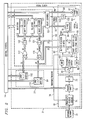
- FIGURE 2 is a block diagram showing the central control circuit 14, the antenna element 21, and the circuit 31 which interfaces the antenna element 21 to the central control circuit 14.
- the circuit 31 has an analog section identified by broken line 61, a digital high speed section identified by broken line 62, a digital reduced speed section identified by broken line 63, and a digital reference signal generator section identified by broken line 64.
- the digital high speed section 62 operates at a clock speed of 10 GHz, and in the disclosed embodiment is implemented with high speed indium phosphide (InP) semiconductor technology of a known type.
- the digital reduced speed section 63 and the digital reference signal generator section 64 each operate at 1/32 the speed of the high speed section 62, in particular at a clock speed 312.5 MHz.
- the sections 63 and 64 are implemented with complementary metal oxide semiconductor (CMOS) integrated circuitry.
- CMOS complementary metal oxide semiconductor
- the analog section 61 includes a transmit/receive circuit 71, a phase shifter 72 and a bandpass filter (BPF) 73 which are coupled in series between the antenna element 21 and the digital high speed section 62.
- the transmit/receive circuit 71 operates in either a transmit mode or a receive mode, based on the state of a transmit/receive control line 76 from the central control circuit 14.
- the phase shifter 72 can induce a phase shift into transmit or receive signals passing through it, the amount of the phase shift being programmable through control lines 77 from the central control circuit 14.
- signals are transmitted and received through the antenna element 21 at a frequency of 7.5 GHz, but it would alternatively be possible to use some other frequency.
- the BPF 73 has a 5 GHz pass band which is centered on a transmit/receive frequency of 7.5 GHz, or in other words has a pass band from about 5 GHz to about 10 GHz.
- a transmit/receive frequency of 7.5 GHz or in other words has a pass band from about 5 GHz to about 10 GHz.
- the characteristics of the pass band could be varied.
- the digital high speed section 62 includes an electronic switch 81 which is controlled by the transmit/receive signal 76 from the central control circuit 14.
- the switch 81 couples the BPF 73 to a digital-to-analog converter (DAC) 82.
- DAC digital-to-analog converter
- ADC analog-to-digital converter
- the DAC 82 has an input which is coupled to an output of a 32-bit bidirectional shift register 86
- the ADC 83 has an output which is coupled to an input of the shift register 86.
- the shift register 86 is supplied with a free-running 10 GHz clock, and the direction in which data shifts through the register 86 is controlled by the state of the transmit/receive line 76 from the central control circuit 14.
- the shift register 86 is associated with a buffer register 87, which is also responsive to the transmit/receive control line 76. Words of 32-bit data can be transferred from the buffer register 87 to the shift register 86 in the transmit mode, and from the shift register 86 to the buffer register 87 in the receive mode.
- a 5-bit counter provides a delay control function which is controlled by a delay control circuit 92 through control lines 93, the delay control circuit 92 being part of the digital reduced speed section 63.
- the counter 91 is clocked with a 10 GHz clock signal, and provides a divide-by-32 function. In particular, on every 32d clock pulse, the counter 91 activates a load control line 94.
- the load control line 94 causes a 32-bit word received in the shift register 86 to be loaded into the buffer register 87.
- the load control line 84 causes the shift register 86 to be loaded with data from the buffer register 87 each time the shift register has finished transmitting 32 bits of data.
- the initial value loaded into the counter 92 by the delay control circuit 92 determines when the load signal 94 is generated in relation to other activity within the circuit 31, thus permitting a programmable time delay to be introduced into data being transmitted or received by the circuit 31.
- the central control circuit 14 outputs a 10 GHz clock signal 96.
- the digital high speed section 62 includes a phase shifter 97, which effects a phase shift of the clock signal 96 by an amount controlled at 98 by the delay control circuit 92. The amount of this phase shift can be different in the various circuits 31-35.
- the output of the phase shifter 97 is a phase-adjusted 10 GHz clock signal 101, which is used to operate the various components of the digital high speed section 62.
- a divide-by-32 circuit 102 converts the 10 GHz clock signal 101 into a 312.5 MHz clock signal 103, which is supplied to the components of the sections 63 and 64.
- the phase shifter 97 can adjust the phases of the 10 GHz clock signal 101 and the 312.5 MHz clock signal 103 by an amount which is less than one period of the 10 GHz clock signal 96. This permits fine tuning of the timing of the operation of the circuit 31 relative to other circuits in the antenna, such as those shown at 32-35 in FIGURE 1 .
- the digital reference signal generator section 64 includes an IREF signal generator 111 and a QREF signal generator 112.
- the IREF generator 111 is used for both transmit and receive, and the QREF generator is used only for receive.
- the central control circuit 14 loads each of the generators 111 and 112 with a respective reference signal, which is 1.7 megabits in length.
- the generator 111 is loaded with such a reference signal.
- Each reference signal may be viewed as a serial stream of binary bits which is 1.7 megabits long, and which is a digitized version of a reference analog waveform.
- the QREF signal and the IREF signal used for the receive mode represent the same analog waveform, but with a phase difference of 90°.
- each of the generators 111 and 112 would output the 1.7 megabits of its respective reference signal one bit at a time, at a rate of 10 GHz.
- the generators 111 and 112 operate at a clock speed of 312.5 MHz, which is 1/32 of 10 GHz. Consequently, in order to output bits at an effective rate of 10 GHz, each of the reference generators 111 and 112 outputs its serial bit stream in successive 32-bit segments at a rate of 312.5 MHz.
- the generators 111 and 112 can be implemented as random access memories which each contain a plurality of 32-bit storage locations, where the 32-bit words in the memory locations are successively accessed and output at a rate of 312.5 MHz.
- the outputs of the IREF generator 111 are coupled to inputs of the buffer register 87, and also to inputs of thirty-two separate exclusive OR gates, which are represented collectively in FIGURE 2 by a single gate symbol 116.
- the outputs of the QREF generator 112 are coupled to inputs of thirty-two exclusive OR gates, which are represented collectively in FIGURE 2 by a single gate symbol 117.
- the 1.7 megabit reference signal in the generator 111 is supplied in 32-bit segments to the buffer register 87, and then to the shift register 86, where the bits are sent serially to the DAC 82 at a rate of 10 GHz.
- the analog output from the DAC 82 is supplied through the switch 81, BPF 73, phase shifter 72 and transmit/receive circuit 71 to the antenna element 21.
- an electromagnetic signal received at the antenna element 21 is converted into an analog signal by the transmit/receive circuit 71, and then passes through the phase shifter 72, BPF 73 and switch 81 to the ADC 83, where it is digitized into a 10 GHz bit stream which is supplied to the shift register 86.
- the bits shifted into the shift register 86 at 10 GHz are supplied in 32-bit segments through the buffer register 87 to the inputs of all of the sixty-four exclusive OR gates 116-117.
- respective bits of one reference signal from the IREF generator 111 are supplied to the inputs of the respective gates 116, and respective bits of the other reference signal from the QREF generator 112 are supplied to the inputs of the respective gates 117.
- Each of the exclusive OR gates 116-117 serves effectively as a 1-bit digital multiplier or mixer, such that the gates 116-117 collectively mix the received signal with the two reference signals from the generators 111 and 112.
- the reference signals from the generators 111 and 112 represent a waveform with a lower frequency than the frequency of the received signal, and thus the gates 116 and 117 effectively implement a down conversion of the frequency of the received signal.
- the outputs of the thirty-two gates 116 are all summed in an adder 121, in order to produce a single 5-bit number which is supplied to inputs of a 5-bit wide shift register 123.
- the outputs of the thirty-two gates 117 are all summed in an adder 122, in order to produce a 5-bit number which is supplied to inputs of a different 5-bit wide shift register 124.
- each 32-bit segment received through the shift register 86 and the buffer register 87 produces one 5-bit number in the shift register 123, and one 5-bit number in the shift register 124.
- the shift registers 123 and 124 each hold a plurality of these numbers.
- a selector 128 can select any one of the 5-bit numbers in the shift register 123, and supply it to the central control circuit 14 as an "I" signal.
- a selector 129 can select any one of the 5-bit numbers in the shift register 124, and supply it to the central control circuit 14 as a "Q" value.
- the particular location along each shift register from which the 5-bit numbers are extracted by the selectors is determined by control lines 131 from the delay control circuit 92. It will be noted that the shift registers 123-124 and the selectors 128-129 effectively implement a programmable delay in the outputs of the adders 121 and 122.
- FIGURE 3 is a timing diagram showing at A an analog waveform 201 which is part of a reference waveform that might be represented digitally by the IREF information in the generator 111.
- B represents a digitized version of the waveform 201, in the form of a plurality of successive samples. If a straight line segment is drawn between the ends of each adjacent pair of the samples at B in FIGURE 3 , these line segments will together define a waveform which approximates the waveform 201.
- the standard DAC would essentially produce a series of pulses as shown at C, where each pulse has a magnitude equal to the magnitude of the corresponding sample, and has a duration equal to the time interval between successive samples.
- FIGURE 4 is a diagrammatic view of several frequency characteristics.
- FIGURE 4 shows at A the frequency spectrum determined by Fourier transform for the digital waveform which is shown at B in FIGURE 3 .
- the presence of energy at negative frequencies is a reflection of the fact that this frequency spectrum is determined mathematically through Fourier analysis, rather by empirical measurement.
- FIGURE 4 shows at B a representation of the pass band of the BPF 73 ( FIGURE 2 ), which corresponds to the desired transmit spectrum.
- reference numeral 206 denotes the portion of the energy which is within the desired transmit spectrum.
- the result will be the frequency spectrum shown at B in FIGURE 4 .
- the magnitude of the energy distribution has a roll-off 207 which is relatively pronounced within the desired transmit spectrum, such that the portion of the energy 208 within the desired transmit spectrum has a distorted spectrum with an asymmetric reduction in magnitude. If the spectrum shown at B in FIGURE 4 was subjected to the band pass filtering characteristic shown at D for the BPF 73, the result would be the spectrum 208 shown at E in FIGURE 4 .
- the DAC 82 of the disclosed embodiment operates differently from a standard DAC.
- the DAC 82 in response to each of the samples shown at D in FIGURE 3 , the DAC 82 would produce the series of pulses shown at D in FIGURE 3 , where each pulse has the same magnitude as the associated sample, but has a duration which is only half the time interval between successive samples.
- the DAC output returns to a predetermined voltage which, in the disclosed embodiment, is zero volts.
- the roll-off characteristic indicated by the broken line 211 maintains a suitable and uniform magnitude throughout the desired transmit spectrum, such that the portion 212 of the energy which is within the desired transmit spectrum has little or no distortion, and conforms relatively closely to the energy characteristic 206 in the spectrum A of FIGURE 4 . If the signal shown at D in FIGURE 3 was subjected to band pass filtering by the filtering characteristic shown at D in FIGURE 4 , the result would be the spectrum shown at F in FIGURE 4 .
- the DAC 82 operates at a frequency of 10 GHz.
- the digital samples supplied to the input of the DAC 82 are each a single binary bit. Each sample can thus only have one of two different states.
- the IREF information output by the generator 111 is a serial stream of binary bits having a length of 1.7 megabits, and is a digital representation of an analog waveform, where each digital sample is a single bit.
- the IREF information was a representation of the waveform 201 shown at A in FIGURE 3
- the digital samples would be as shown at E in FIGURE 3 , rather than at B.
- the samples at E each have a uniform magnitude, although some are positive and some are negative. Those with a positive magnitude would each be represented by a binary "1", and those with a negative magnitude would each be represented by a binary "0". In a sense, this is simply the sign bit of each sample shown at B in FIGURE 3 , since each sample at B with a positive magnitude has a sign bit of "1", and each sample at B with a negative magnitude has a sign bit of "0".
- the samples shown at E in FIGURE 3 are applied in sequence to the input of the DAC 82, the resulting output would be as shown at F in FIGURE 3 .
- the waveform at F in FIGURE 3 enjoys the same favorable roll-off characteristic which is shown at 211 in FIGURE 4 , rather than the distorted roll-off characteristic shown at 207 in FIGURE 4 .
- the reference waveform represented in digital form by the IREF information in generator 111 is configured in the disclosed embodiment as a series of successive samples which are each one binary bit. That is, each sample is either a binary "1" or a binary "0".
- the reference waveform 201 of FIGURE 3 will be represented by samples such as those shown diagrammatically at E in FIGURE 3 . If a waveform is reconstructed directly from the samples shown E in FIGURE 3 , it will have generally the shape of the waveform 241 shown at G in FIGURE 3 .
- the waveform 241 is, of course, an approximation of the waveform 201, and is not identical to the waveform 201. In essence, the waveform 241 represents the waveform 201 with the addition of various harmonics. In other words, when a waveform such as that shown at 201 is digitized using 1-bit samples, the resulting digital signal includes unwanted harmonics.
- the disclosed embodiment includes provisions which substantially reduce these unwanted harmonics. This is explained in more detail with reference to FIGURE 5 .
- FIGURE 5 is a block diagram showing two of the antenna elements 21 and 22 from FIGURE 1 , and the associated circuits 31 and 32.
- the circuit 31 has already been described in detail with reference to FIGURE 2 , and selected components of this circuit are depicted in FIGURE 5 , including the transmit/receive circuit 71, phase shifter 72, BPF 73, DAC 82, shift register 86, and IREF generator 111.
- the circuit 32 is identical to the circuit 31, and FIGURE 5 thus shows components 251-253 and 256-258 of the circuit 32 which are respectively equivalent to the components 71-73, 82, 86 and 111 of the circuit 31.
- the antenna system is to transmit electromagnetic signals corresponding to a reference waveform, which is the waveform 201 of FIGURE 3 .
- this waveform would be digitized into 1-bit samples as shown at E in FIGURE 3 , in order to obtain the IREF information, and the same IREF information would be stored in each of the IREF generators 111 and 258.
- the timing of the shift registers 86 and 257 would be controlled to introduce appropriate respective time delays into each signal so that, when each signal is transmitted from a respective antenna element 21 or 22, the resulting wavefront will be directed or steered in the desired direction relative to the antenna.
- the disclosed embodiment takes a different approach which reduces the unwanted harmonics.
- the waveforms stored in the generators 111 and 258 are not identical. Instead, the reference waveform 201 is given an arbitrary phase shift ⁇ 1 relative to a reference, and is then digitized into the 1-bit samples which are stored in the IREF generator 111. Separately, the same reference waveform 201 is given a different phase shift ⁇ 2 with respect to the same reference, and is then digitized into 1-bit samples which are stored in the IREF generator 258.
- the shift registers 86 and 257 then impart appropriate time delays to the respective signals in order to properly steer the waveform which is to be transmitted.
- the digital signals from the shift registers are then converted into respective analog signals by the DAC 82 and DAC 256, and then the resulting analog signals are subjected to bandpass filtering at 73 and 253.
- the digital reference signal is effectively a square wave signal
- odd harmonics are more dominant than even harmonics.
- the harmonics do not receive the same phase shift as the fundamental signal. More specifically, and with reference to block 271 in FIGURE 5 , at the output of BPF 73 the fundamental signal will have a phase shift of ⁇ 1, the third harmonic will have a phase shift of 3 ⁇ 1, the fifth harmonic will have a phase shift of 5 ⁇ 1, the seventh harmonic will have phase shift of 7 ⁇ 1, and so forth.
- the fundamental will have a phase shift of ⁇ 2
- the third harmonic will have a phase shift of 3 ⁇ 2
- the fifth harmonic will have a phase shift of 5 ⁇ 2
- the seventh harmonic will have a phase shift of 7 ⁇ 2, and so forth.
- the phase shifter 72 in the circuit 31 is set to implement a phase shift of - ⁇ 1, which is opposite and equal to the phase shift ⁇ 1 introduced before digitization of the IREF information for the generator 111.
- the phase shifter 252 in the circuit 32 is set to implement a phase shift of - ⁇ 2, which is opposite and equal to the phase shift ⁇ 2 introduced before digitization of the IREF information for the generator 258. Therefore, and with reference to block 273 in FIGURE 5 , at the output of the phase shifter 72 the fundamental will have a phase shift of zero, the third harmonic will have a phase shift of 2 ⁇ 1, the fifth harmonic will have a phase shift of 4 ⁇ 1, the seventh harmonic will have a phase shift of 6 ⁇ 1, and so forth.
- the fundamental will have a phase shift of zero
- the third harmonic will have a phase shift of 2 ⁇ 2
- the fifth harmonic will have a phase shift of 4 ⁇ 2
- the seventh harmonic will have a phase shift of 6 ⁇ 2, and so forth.
- FIGURE 5 shows only two antenna elements 21 and 22 with their associated circuits 31 and 32, but it will be recognized that where a variety of phase shifts are used for all of the respective antenna elements in the array, the result will be non-coherent addition of the third harmonics in an effective and efficient manner that causes the wavefront for the fundamental to have little or no significant presence of the third harmonic.
- the other harmonics are also out of phase and tend to add non-coherently in free space, and thus have little or no significant presence in the wavefront for the fundamental.
- phase shifters 72 and 252 can be used in the receive mode to introduce respective different phase shifts into respective signals received by the antenna elements 21 and 22, after which these phase-shifted signals are digitized into 1-bit samples. As discussed above, this digitization technique introduces unwanted harmonics. Thereafter, these signals are converted into the I and Q signals which are delivered to the central control circuit 14 ( FIGUREs 1 and 2 ).
- the central control circuit 14 can apply respective phase shifts equal and opposite to those introduced by the phase shifters 72 and 252, and can then combine the resulting signals, so that the components representing the fundamental add coherently and the components representing harmonics add non-coherently.
- the present invention provides a number of technical advantages.
- One such technical advantage results from the use of low precision digital devices to generates a transmit waveform in a highly distributed manner.
- This digital generation of waveforms involves circuitry of reduced size, weight, power and cost in comparison to pre-existing circuits for analog waveform generation. Respective time delays for respective component signals are readily accomplished in the digital domain using shift registers and other logic.
- a related advantage is that, in the context of a radar system, the circuitry of the antenna is primarily digital circuitry rather than radio frequency circuitry, and interfaces between the antenna and a central control system are all digital.
- Another advantage results from the use of digital-to-analog converters that produce for each sample a pulse having a duration less than the time interval between samples, the output of the converter returning to zero during the time interval between adjacent pulses.
- This technique permits transmission of a waveform which closely approximates the quality of the waveform that would be generated and transmitted by pre-existing analog techniques, but with significant reductions in size, weight, power and cost for the relevant circuitry.
- a further advantage results from the fact that a separate transmitter/receiver circuit is provided for each antenna element, whereas the traditional analog approach uses a single transmitter/receiver to handle a single signal which is subjected to respective phase shifts or time delays between the transmitter/receiver and respective antenna elements. Consequently, the disclosed embodiment provides capabilities which are not present in pre-existing analog configurations. For example, it would be possible to use only a subset of the antenna elements in the antenna array. Alternatively, different subsets of the antenna elements could be used at the same time to transmit different waveforms.
- Still another advantage results in the receive mode, when a respective phase shift is introduced into the analog signal from each antenna element before it is digitized, and then the same phase shift is removed after digitization.
- the components for the fundamental add coherently whereas the components for harmonics add non-coherently, thereby greatly reducing harmonics introduced by the digitization. This is particularly advantageous where the digitization process involves the use of one-bit samples.
Landscapes
- Variable-Direction Aerials And Aerial Arrays (AREA)
- Radar Systems Or Details Thereof (AREA)
- Burglar Alarm Systems (AREA)
Claims (26)
- Dispositif pour traiter des signaux dans un système de réseau d'antennes, comprenant une pluralité d'éléments d'antenne (21-25) connectés à une pluralité de circuits (31-35), grâce à quoi chaque circuit (31-35) est associé à un élément d'antenne respectif (21-25),
caractérisé en ce que, dans un mode d'émission, chaque circuit (31-35) comprend :une section de générateur de signaux (111 ; 258) qui délivre des premier et second signaux numériques, ledit premier signal numérique représentant une partie fondamentale et des harmoniques indésirables d'une forme d'onde de référence prédéterminée avec un premier déphasage (φ1) qui lui est communiqué en relation avec ladite forme d'onde de référence prédéterminée, ledit second signal numérique représentant ladite partie fondamentale de référence et les harmoniques indésirables de ladite forme d'onde de référence prédéterminée avec un second déphasage (φ2) qui lui est communiqué en relation avec ladite forme d'onde de référence prédéterminée, ledit second déphasage (φ2) étant différent dudit premier déphasage (φ1);une section de convertisseur numérique-analogique (82 ; 256) qui convertit lesdits premier et second signaux numériques, respectivement, en des premier et second signaux analogiques ; etune section de déphasage (72 ; 252) qui produit un premier signal ajusté en communiquant audit premier signal analogique un déphasage (-φ1) qui est sensiblement égal et opposé audit premier déphasage (φ1), et qui produit un second signal ajusté en communiquant audit second signal analogique un déphasage (-φ2) qui est sensiblement égal et opposé audit second déphasage (φ2), afin de permettre auxdites parties fondamentales des premier et second signaux ajustés de s'ajouter de manière cohérente dans l'espace libre et aux harmoniques indésirables des premier et second signaux ajustés de s'ajouter de manière non cohérente dans l'espace libre. - Dispositif selon la revendication 1, incluant un circuit d'émission/réception (71 ; 251) qui émet des premier et second signaux électromagnétiques qui incluent, respectivement, lesdits premier et second signaux ajustés.
- Dispositif selon la revendication 2, dans lequel ledit circuit d'émission/réception (71 ; 251) inclut des premier et second éléments d'antenne (21 ; 22) qui sont physiquement espacés l'un de l'autre, lesdits premier et second signaux électromagnétiques étant respectivement émis au travers desdits premier et second éléments d'antenne (21 ; 22).
- Dispositif selon la revendication 1, incluant une section de filtre (73 ; 253) qui effectue un filtrage passe-bande dudit premier signal analogique avant que ledit premier signal analogique ne soit transmis à ladite section de déphasage (72 ; 252), et qui effectue un filtrage passe-bande dudit second signal analogique avant que ledit second signal analogique ne soit transmis à ladite section de déphasage (72 ; 252).
- Dispositif selon la revendication 1, dans lequel lesdits premier et second signaux numériques ont chacun une pluralité d'états successifs, chacun desdits états étant l'un sélectionné de premier et second états prédéterminés qui sont différents.
- Dispositif selon la revendication 1, dans lequel les premier et second signaux numériques sont une série d'échantillons à un bit successifs.
- Dispositif selon la revendication 1,
dans lequel lesdits premier et second signaux numériques ont chacun une pluralité d'états successifs;
dans lequel ladite section de convertisseur numérique-analogique (82 ; 256) génère pour chaque dit état dudit premier signal numérique une impulsion correspondante respective dudit premier signal analogique qui a une durée inférieure à la durée de l'état correspondant, ladite section de convertisseur numérique-analogique (82 ; 256) délivrant une tension prédéterminée entre lesdites impulsions successives dudit premier signal analogique ; et
dans lequel ladite section de convertisseur numérique-analogique (82 ; 256) génère pour chaque dit état dudit second signal numérique une impulsion correspondante respective dudit second signal analogique qui a une durée inférieure à la durée de l'état correspondant, ladite section de convertisseur numérique-analogique (82 ; 256) délivrant une tension prédéterminée entre lesdites impulsions successives dudit second signal analogique. - Dispositif selon la revendication 6, incluant un circuit d'émission/réception (71 ; 251) qui émet un signal électromagnétique pour chacun desdits premier et second signaux ajustés.
- Dispositif selon la revendication 8, incluant une section de filtre passe-bande (73 ; 253) qui traite lesdits premier et second signaux analogiques avant l'émission dudit signal analogique par ladite section d'émetteur.
- Dispositif selon la revendication 6, dans lequel ladite tension prédéterminée est de zéro volt environ.
- Dispositif selon la revendication 6, dans lequel chaque dite impulsion a une durée qui est environ la moitié de la durée de l'état correspondant desdits premier et second signaux numériques.
- Dispositif selon la revendication 6, dans lequel chaque dit état desdits premier et second signaux numériques est l'un sélectionné des premier et second états prédéterminés qui sont différents.
- Dispositif selon la revendication 12, dans lequel ladite section de convertisseur numérique-analogique (82 ; 256) génère une impulsion positive ayant une amplitude prédéterminée lorsque l'état correspondant desdits premier et second signaux numériques est ledit premier état prédéterminé, et génère une impulsion négative ayant ladite amplitude prédéterminée lorsque l'état correspondant desdits premier et second signaux numériques est ledit second état prédéterminé ; et dans lequel ladite tension prédéterminée est de zéro volt environ.
- Dispositif selon la revendication 13, dans lequel chaque dite impulsion a une durée qui est environ la moitié de la durée de l'état correspondant desdits premier et second signaux numériques respectifs.
- Dispositif selon la revendication 14, dans lequel chaque dite impulsion a approximativement une forme d'onde carrée.
- Dispositif selon la revendication 1, incluant une section de retard sous la forme d'un registre à décalage (86 ; 257) utilisé pour introduire des retards respectifs dans les premier et second signaux numériques de manière à diriger les formes d'onde de référence prédéterminées suivant une direction appropriée.
- Dispositif selon la revendication 16, incluant un compteur de retard (91) utilisé pour commander les retards introduits par la section de retard (86 ; 257).
- Dispositif selon la revendication 17, dans lequel le compteur de retard (91) active une ligne de commande de charge (94) pour amener des données à être chargées dans la section de retard (86 ; 257).
- Dispositif selon la revendication 18, incluant un contrôleur de retard (92) utilisé pour fixer une valeur de retard dans le compteur de retard (91).
- Procédé pour traiter des signaux dans un système de réseau d'antennes, comprenant les étapes consistant :à produire des premier et second signaux numériques, ledit premier signal numérique représentant une partie fondamentale et des harmoniques indésirables d'une forme d'onde de référence prédéterminée avec un premier déphasage (φ1) qui lui est communiqué en relation avec ladite forme d'onde de référence prédéterminée, ledit second signal numérique représentant ladite partie fondamentale et les harmoniques indésirables de ladite forme d'onde de référence prédéterminée avec un second déphasage (φ2) qui lui est communiqué en relation avec ladite forme d'onde de référence prédéterminée, ledit second déphasage (φ2) étant différent dudit premier déphasage (φ1) ;à convertir lesdits premier et second signaux numériques, respectivement, en des premier et second signaux analogiques ;à communiquer audit premier signal analogique un déphasage (-φ1) qui est sensiblement égal et opposé audit premier déphasage (φ1) de manière à obtenir un premier signal ajusté, et à communiquer audit second signal analogique un déphasage (-φ2) qui est sensiblement égal et opposé audit second déphasage (φ2) de manière à obtenir un second signal ajusté, afin de permettre auxdites parties fondamentales des premier et second signaux ajustés de s'ajouter de manière cohérente dans l'espace libre et aux harmoniques indésirables de s'ajouter de manière non cohérente dans l'espace libre.
- Procédé selon la revendication 20, dans lequel ladite étape consistant à produire lesdits premier et second signaux numériques inclut l'étape consistant à configurer lesdits premier et second signaux numériques pour que chacun ait une pluralité d'états successifs, chacun desdits états étant l'un sélectionné des premier et second états prédéterminés qui sont différents.
- Procédé selon la revendication 20, incluant l'introduction de retards respectifs dans les premier et second signaux numériques de manière à diriger les formes d'onde prédéterminées suivant une direction appropriée.
- Procédé selon la revendication 20,
dans lequel ladite étape consistant à produire lesdits premier et second signaux numériques inclut l'étape consistant à configurer lesdits premier et second signaux numériques pour que chacun ait une pluralité d'états successifs ;
dans lequel ladite étape de conversion inclut la génération pour chaque dit état dudit premier signal numérique d'une impulsion correspondante respective dudit premier signal analogique qui a une durée inférieure à la durée de l'état correspondant, et la délivrance d'une tension prédéterminée entre lesdites impulsions successives dudit premier signal analogique ; et
dans lequel ladite étape de conversion inclut la génération pour chaque dit état dudit second signal numérique d'une impulsion correspondante respective dudit second signal analogique qui a une durée inférieure à la durée de l'état correspondant, et la délivrance d'une tension prédéterminée entre lesdites impulsions successives dudit second signal analogique. - Procédé selon la revendication 23, dans lequel ladite étape consistant à générer des impulsions est mise en oeuvre de telle manière que chaque dite impulsion a une durée qui est environ la moitié de la durée de l'état correspondant desdits premier et second signaux numériques.
- Procédé selon la revendication 23, dans lequel ladite étape consistant à produire lesdits premier et second signaux numériques est mise en oeuvre de telle manière que chaque dit état desdits premier et second signaux numériques est l'un sélectionné des premier et second états prédéterminés qui sont différents.
- Procédé selon la revendication 25, dans lequel ladite étape consistant à générer des impulsions inclut les étapes consistant à générer une impulsion positive ayant une amplitude prédéterminée lorsque l'état correspondant desdits premier et second signaux numériques respectifs est ledit premier état prédéterminé, et à générer une impulsion négative ayant ladite amplitude prédéterminée lorsque l'état correspondant desdits premier et second signaux numériques respectifs est ledit second état prédéterminé.
Applications Claiming Priority (3)
| Application Number | Priority Date | Filing Date | Title |
|---|---|---|---|
| US28009 | 1998-02-23 | ||
| US10/028,009 US7079588B1 (en) | 2001-12-21 | 2001-12-21 | Method and apparatus for processing signals in an array antenna system |
| PCT/US2002/040694 WO2003061070A1 (fr) | 2001-12-21 | 2002-12-19 | Procedes et appareil de traitement de signaux dans un systeme d'antenne reseau |
Publications (3)
| Publication Number | Publication Date |
|---|---|
| EP1456904A1 EP1456904A1 (fr) | 2004-09-15 |
| EP1456904B1 true EP1456904B1 (fr) | 2009-02-18 |
| EP1456904B8 EP1456904B8 (fr) | 2009-04-22 |
Family
ID=21841035
Family Applications (1)
| Application Number | Title | Priority Date | Filing Date |
|---|---|---|---|
| EP02797429A Expired - Lifetime EP1456904B8 (fr) | 2001-12-21 | 2002-12-19 | Procedes et appareil de traitement de signaux dans un systeme d'antenne reseau |
Country Status (7)
| Country | Link |
|---|---|
| US (1) | US7079588B1 (fr) |
| EP (1) | EP1456904B8 (fr) |
| AT (1) | ATE423402T1 (fr) |
| AU (1) | AU2002361792A1 (fr) |
| DE (1) | DE60231242D1 (fr) |
| ES (1) | ES2322569T3 (fr) |
| WO (1) | WO2003061070A1 (fr) |
Families Citing this family (7)
| Publication number | Priority date | Publication date | Assignee | Title |
|---|---|---|---|---|
| US7627056B1 (en) * | 2002-03-29 | 2009-12-01 | Scientific Research Corporation | System and method for orthogonally multiplexed signal transmission and reception on a non-contiguous spectral basis |
| US20070111679A1 (en) * | 2005-11-16 | 2007-05-17 | Thompson Bruce M | Method and apparatus for vector signal processing |
| US7173427B1 (en) * | 2005-12-23 | 2007-02-06 | Kabushiki Kaisha Toshiba | Magnetic resonance imaging apparatus and magnetic resonance imaging method |
| RU2392704C1 (ru) * | 2008-10-09 | 2010-06-20 | ОАО "Уральское проектно-конструкторское бюро "Деталь" | Способ повышения широкополосности приемопередающего модуля фазированной антенной решетки, использующего генерацию сигналов методом прямого цифрового синтеза, и варианты его реализации |
| US8274425B2 (en) * | 2010-12-29 | 2012-09-25 | Raytheon Company | Single channel semi-active radar seeker |
| DE102012009402B3 (de) * | 2012-05-10 | 2013-07-04 | Eads Deutschland Gmbh | Phased-Array Antenne und Verfahren zur Verarbeitung von Empfangssignalen in einer Phased-Array Antenne |
| US10164335B2 (en) * | 2015-09-25 | 2018-12-25 | Rockwell Collins, Inc. | Unit cell filtering and diplexing for electronically scanned arrays |
Family Cites Families (39)
| Publication number | Priority date | Publication date | Assignee | Title |
|---|---|---|---|---|
| US3887918A (en) | 1973-05-09 | 1975-06-03 | Itt | Multi-level digital coincidence detection |
| GB2130798B (en) | 1982-10-06 | 1986-02-12 | Standard Telephones Cables Ltd | Digital beam-forming radar |
| US4749995A (en) | 1985-02-26 | 1988-06-07 | Westinghouse Electric Corp. | Phased array radar antenna system |
| CA1232059A (fr) | 1985-03-21 | 1988-01-26 | Donald C. Knudsen | Controleur de retard numerique pour generateurs de signaux sonar et radar |
| US4839652A (en) | 1987-06-01 | 1989-06-13 | General Electric Company | Method and apparatus for high speed digital phased array coherent imaging system |
| US4886069A (en) | 1987-12-21 | 1989-12-12 | General Electric Company | Method of, and apparatus for, obtaining a plurality of different return energy imaging beams responsive to a single excitation event |
| US5223843A (en) | 1988-01-05 | 1993-06-29 | Rockwell International Corporation | High performance global positioning system receiver means and method |
| FR2651609B1 (fr) | 1989-09-01 | 1992-01-03 | Thomson Csf | Commande de pointage pour systeme d'antenne a balayage electronique et formation de faisceau par le calcul. |
| US4983970A (en) | 1990-03-28 | 1991-01-08 | General Electric Company | Method and apparatus for digital phased array imaging |
| US5271034A (en) | 1991-08-26 | 1993-12-14 | Avion Systems, Inc. | System and method for receiving and decoding global positioning satellite signals |
| GB9126944D0 (en) | 1991-12-19 | 1992-02-19 | Secr Defence | A digital beamforming array |
| US5475392A (en) | 1993-09-30 | 1995-12-12 | Hughes Aircraft Company | Frequency translation of true time delay signals |
| US5517529A (en) | 1993-10-18 | 1996-05-14 | Westinghouse Electric Corp. | UHF/L-Band monolithic direct digital receiver |
| US5414433A (en) | 1994-02-16 | 1995-05-09 | Raytheon Company | Phased array radar antenna with two-stage time delay units |
| US5903823A (en) * | 1995-09-19 | 1999-05-11 | Fujitsu Limited | Radio apparatus with distortion compensating function |
| US5917447A (en) | 1996-05-29 | 1999-06-29 | Motorola, Inc. | Method and system for digital beam forming |
| US5930299A (en) * | 1996-08-08 | 1999-07-27 | Motorola, Inc. | Digital modulator with compensation and method therefor |
| US6141371A (en) | 1996-12-18 | 2000-10-31 | Raytheon Company | Jamming suppression of spread spectrum antenna/receiver systems |
| JPH10190521A (ja) * | 1996-12-20 | 1998-07-21 | Fujitsu Ltd | 無線通信装置及び無線通信システム |
| US5764187A (en) | 1997-01-21 | 1998-06-09 | Ail Systems, Inc. | Direct digital synthesizer driven phased array antenna |
| IT1293059B1 (it) | 1997-06-24 | 1999-02-11 | Space Engineering Spa | Radar bi-statico digitale a spettro espanso |
| US6191735B1 (en) | 1997-07-28 | 2001-02-20 | Itt Manufacturing Enterprises, Inc. | Time delay apparatus using monolithic microwave integrated circuit |
| US6240122B1 (en) * | 1997-09-02 | 2001-05-29 | Fujitsu Limited | Receiving apparatus of code spread communication type |
| US6160505A (en) | 1998-02-24 | 2000-12-12 | At&T Corp | Method and apparatus for converting an analog signal to a digital signal |
| JP4015750B2 (ja) * | 1998-05-14 | 2007-11-28 | 株式会社東芝 | アクティブアレイアンテナシステム |
| US6052085A (en) | 1998-06-05 | 2000-04-18 | Motorola, Inc. | Method and system for beamforming at baseband in a communication system |
| JP3183266B2 (ja) * | 1998-08-18 | 2001-07-09 | 日本電気株式会社 | 自動周波数制御回路 |
| KR20000024709A (ko) * | 1998-10-01 | 2000-05-06 | 정선종 | 대역저감 다반송파 무선송수신장치 및 그 방법 |
| JP3742731B2 (ja) * | 1998-12-18 | 2006-02-08 | アイコム株式会社 | Msk変調器、角度変調器、ディジタル信号発生器、msk変調方法及び記録媒体 |
| US6430232B1 (en) * | 1999-01-26 | 2002-08-06 | Trw Inc. | Phase constellation modulator |
| US6693590B1 (en) * | 1999-05-10 | 2004-02-17 | Raytheon Company | Method and apparatus for a digital phased array antenna |
| JP3910443B2 (ja) * | 1999-06-09 | 2007-04-25 | 三菱電機株式会社 | 自動周波数制御装置 |
| US6259253B1 (en) * | 1999-06-10 | 2001-07-10 | Ohio State University Research Foundation | MRI transceiver |
| JP3386114B2 (ja) * | 1999-11-05 | 2003-03-17 | 日本電気株式会社 | 復調装置及び方法 |
| US7123882B1 (en) | 2000-03-03 | 2006-10-17 | Raytheon Company | Digital phased array architecture and associated method |
| US6693980B1 (en) * | 2000-09-18 | 2004-02-17 | Telasic Communications, Inc. | Wideband fast-hopping receiver front-end and mixing method |
| GB0104535D0 (en) * | 2001-02-23 | 2001-04-11 | Univ Bristol | Digital cartesian loop |
| US6771709B2 (en) * | 2001-10-16 | 2004-08-03 | Her Majesty The Queen In Right Of Canada, As Represented By The Minister Of Industry | System and method for direct transmitter self-calibration |
| US7058139B2 (en) * | 2001-11-16 | 2006-06-06 | Koninklijke Philips Electronics N.V. | Transmitter with transmitter chain phase adjustment on the basis of pre-stored phase information |
-
2001
- 2001-12-21 US US10/028,009 patent/US7079588B1/en not_active Expired - Lifetime
-
2002
- 2002-12-19 AT AT02797429T patent/ATE423402T1/de not_active IP Right Cessation
- 2002-12-19 EP EP02797429A patent/EP1456904B8/fr not_active Expired - Lifetime
- 2002-12-19 AU AU2002361792A patent/AU2002361792A1/en not_active Abandoned
- 2002-12-19 DE DE60231242T patent/DE60231242D1/de not_active Expired - Lifetime
- 2002-12-19 ES ES02797429T patent/ES2322569T3/es not_active Expired - Lifetime
- 2002-12-19 WO PCT/US2002/040694 patent/WO2003061070A1/fr not_active Ceased
Also Published As
| Publication number | Publication date |
|---|---|
| WO2003061070A1 (fr) | 2003-07-24 |
| AU2002361792A1 (en) | 2003-07-30 |
| ES2322569T3 (es) | 2009-06-23 |
| EP1456904B8 (fr) | 2009-04-22 |
| DE60231242D1 (de) | 2009-04-02 |
| ATE423402T1 (de) | 2009-03-15 |
| EP1456904A1 (fr) | 2004-09-15 |
| US7079588B1 (en) | 2006-07-18 |
Similar Documents
| Publication | Publication Date | Title |
|---|---|---|
| US6701141B2 (en) | Mixed signal true time delay digital beamformer | |
| Garrod | Digital modules for phased array radar | |
| US5077562A (en) | Digital beam-forming technique using temporary noise injection | |
| US4965602A (en) | Digital beamforming for multiple independent transmit beams | |
| CN111370873B (zh) | 基于时间调制阵列的高效率相位调控系统 | |
| EP1281213B1 (fr) | Recalage de donnees d'antenne en reseau a commande de phase | |
| JPH11509000A (ja) | フェーズドアレイレーダ用回路モジュール | |
| EP1266427B1 (fr) | Architecture de reseau a commande de phase numerique et procede associe | |
| US7079588B1 (en) | Method and apparatus for processing signals in an array antenna system | |
| KR102341508B1 (ko) | 직접 디지털 합성 기반 위상 쉬프트 디지털 빔포밍 | |
| Steiner et al. | A 1.6-GHz sub-Nyquist-sampled wideband beamformer on an RFSoC | |
| US12425078B2 (en) | Digital beam forming | |
| US20190089054A1 (en) | Techniques and Methods for Adaptive Removal of Analog Phase Errors in Frequency Division Multiplexed Digital Beam-Formers | |
| CA1253959A (fr) | Alimentation d'antenne reseau a commande de phase | |
| Pulipati et al. | Design considerations and FPGA implementation of a wideband all-digital transmit beamformer with 50% fractional bandwidth | |
| Provan et al. | Farrow-based true time-delay FPGA wideband digital beamforming architecture | |
| Chen et al. | Implementation of Wideband DBF for Large Aperture Phased Array Radar Based on FPGA | |
| Joseph et al. | Subsampling time-modulated array for reduced hardware down conversion and beamforming | |
| Tanaka et al. | Digital signal processor for digital multi-beam forming antenna in mobile communication | |
| Liu et al. | Practical beamforming technologies for wideband digital array radar | |
| Xia et al. | A novel method of space-borne cognitive SAR signal generation based on FPGA and DDS | |
| Dasan et al. | RFSoC Based Beam Squint Mitigation Technique for Wideband Digital Active Phased Array Radar Applications | |
| Rossi et al. | Beamforming in a Multifunctional Fully Digital Phased Array | |
| Xu et al. | A Multiply-and-Accumulate SAR-ADC-Based Hybrid Slepian Beamformer | |
| Yang et al. | Digital Beamforming Capacity Assessment of RFSoC for L-Band SAR Applications |
Legal Events
| Date | Code | Title | Description |
|---|---|---|---|
| PUAI | Public reference made under article 153(3) epc to a published international application that has entered the european phase |
Free format text: ORIGINAL CODE: 0009012 |
|
| 17P | Request for examination filed |
Effective date: 20040709 |
|
| AK | Designated contracting states |
Kind code of ref document: A1 Designated state(s): AT BE BG CH CY CZ DE DK EE ES FI FR GB GR IE IT LI LU MC NL PT SE SI SK TR |
|
| GRAP | Despatch of communication of intention to grant a patent |
Free format text: ORIGINAL CODE: EPIDOSNIGR1 |
|
| GRAS | Grant fee paid |
Free format text: ORIGINAL CODE: EPIDOSNIGR3 |
|
| GRAA | (expected) grant |
Free format text: ORIGINAL CODE: 0009210 |
|
| AK | Designated contracting states |
Kind code of ref document: B1 Designated state(s): AT BE BG CH CY CZ DE DK EE ES FI FR GB GR IE IT LI LU MC NL PT SE SI SK TR |
|
| REG | Reference to a national code |
Ref country code: GB Ref legal event code: FG4D |
|
| REG | Reference to a national code |
Ref country code: CH Ref legal event code: EP |
|
| REG | Reference to a national code |
Ref country code: IE Ref legal event code: FG4D |
|
| REF | Corresponds to: |
Ref document number: 60231242 Country of ref document: DE Date of ref document: 20090402 Kind code of ref document: P |
|
| RAP2 | Party data changed (patent owner data changed or rights of a patent transferred) |
Owner name: RAYTHEON COMPANY |
|
| NLT2 | Nl: modifications (of names), taken from the european patent patent bulletin |
Owner name: RAYTHEON COMPANY Effective date: 20090408 |
|
| REG | Reference to a national code |
Ref country code: ES Ref legal event code: FG2A Ref document number: 2322569 Country of ref document: ES Kind code of ref document: T3 |
|
| PG25 | Lapsed in a contracting state [announced via postgrant information from national office to epo] |
Ref country code: FI Free format text: LAPSE BECAUSE OF FAILURE TO SUBMIT A TRANSLATION OF THE DESCRIPTION OR TO PAY THE FEE WITHIN THE PRESCRIBED TIME-LIMIT Effective date: 20090218 Ref country code: SI Free format text: LAPSE BECAUSE OF FAILURE TO SUBMIT A TRANSLATION OF THE DESCRIPTION OR TO PAY THE FEE WITHIN THE PRESCRIBED TIME-LIMIT Effective date: 20090218 |
|
| PG25 | Lapsed in a contracting state [announced via postgrant information from national office to epo] |
Ref country code: AT Free format text: LAPSE BECAUSE OF FAILURE TO SUBMIT A TRANSLATION OF THE DESCRIPTION OR TO PAY THE FEE WITHIN THE PRESCRIBED TIME-LIMIT Effective date: 20090218 Ref country code: SE Free format text: LAPSE BECAUSE OF FAILURE TO SUBMIT A TRANSLATION OF THE DESCRIPTION OR TO PAY THE FEE WITHIN THE PRESCRIBED TIME-LIMIT Effective date: 20090518 |
|
| PG25 | Lapsed in a contracting state [announced via postgrant information from national office to epo] |
Ref country code: BE Free format text: LAPSE BECAUSE OF FAILURE TO SUBMIT A TRANSLATION OF THE DESCRIPTION OR TO PAY THE FEE WITHIN THE PRESCRIBED TIME-LIMIT Effective date: 20090218 |
|
| PG25 | Lapsed in a contracting state [announced via postgrant information from national office to epo] |
Ref country code: DK Free format text: LAPSE BECAUSE OF FAILURE TO SUBMIT A TRANSLATION OF THE DESCRIPTION OR TO PAY THE FEE WITHIN THE PRESCRIBED TIME-LIMIT Effective date: 20090218 Ref country code: CZ Free format text: LAPSE BECAUSE OF FAILURE TO SUBMIT A TRANSLATION OF THE DESCRIPTION OR TO PAY THE FEE WITHIN THE PRESCRIBED TIME-LIMIT Effective date: 20090218 Ref country code: EE Free format text: LAPSE BECAUSE OF FAILURE TO SUBMIT A TRANSLATION OF THE DESCRIPTION OR TO PAY THE FEE WITHIN THE PRESCRIBED TIME-LIMIT Effective date: 20090218 Ref country code: PT Free format text: LAPSE BECAUSE OF FAILURE TO SUBMIT A TRANSLATION OF THE DESCRIPTION OR TO PAY THE FEE WITHIN THE PRESCRIBED TIME-LIMIT Effective date: 20090727 |
|
| PG25 | Lapsed in a contracting state [announced via postgrant information from national office to epo] |
Ref country code: SK Free format text: LAPSE BECAUSE OF FAILURE TO SUBMIT A TRANSLATION OF THE DESCRIPTION OR TO PAY THE FEE WITHIN THE PRESCRIBED TIME-LIMIT Effective date: 20090218 |
|
| PLBE | No opposition filed within time limit |
Free format text: ORIGINAL CODE: 0009261 |
|
| STAA | Information on the status of an ep patent application or granted ep patent |
Free format text: STATUS: NO OPPOSITION FILED WITHIN TIME LIMIT |
|
| 26N | No opposition filed |
Effective date: 20091119 |
|
| PG25 | Lapsed in a contracting state [announced via postgrant information from national office to epo] |
Ref country code: BG Free format text: LAPSE BECAUSE OF FAILURE TO SUBMIT A TRANSLATION OF THE DESCRIPTION OR TO PAY THE FEE WITHIN THE PRESCRIBED TIME-LIMIT Effective date: 20090518 |
|
| PG25 | Lapsed in a contracting state [announced via postgrant information from national office to epo] |
Ref country code: MC Free format text: LAPSE BECAUSE OF NON-PAYMENT OF DUE FEES Effective date: 20100701 |
|
| REG | Reference to a national code |
Ref country code: CH Ref legal event code: PL |
|
| PG25 | Lapsed in a contracting state [announced via postgrant information from national office to epo] |
Ref country code: GR Free format text: LAPSE BECAUSE OF FAILURE TO SUBMIT A TRANSLATION OF THE DESCRIPTION OR TO PAY THE FEE WITHIN THE PRESCRIBED TIME-LIMIT Effective date: 20090519 Ref country code: CH Free format text: LAPSE BECAUSE OF NON-PAYMENT OF DUE FEES Effective date: 20091231 Ref country code: LI Free format text: LAPSE BECAUSE OF NON-PAYMENT OF DUE FEES Effective date: 20091231 Ref country code: IE Free format text: LAPSE BECAUSE OF NON-PAYMENT OF DUE FEES Effective date: 20091219 |
|
| PG25 | Lapsed in a contracting state [announced via postgrant information from national office to epo] |
Ref country code: LU Free format text: LAPSE BECAUSE OF NON-PAYMENT OF DUE FEES Effective date: 20091219 |
|
| PG25 | Lapsed in a contracting state [announced via postgrant information from national office to epo] |
Ref country code: TR Free format text: LAPSE BECAUSE OF FAILURE TO SUBMIT A TRANSLATION OF THE DESCRIPTION OR TO PAY THE FEE WITHIN THE PRESCRIBED TIME-LIMIT Effective date: 20090218 |
|
| PG25 | Lapsed in a contracting state [announced via postgrant information from national office to epo] |
Ref country code: CY Free format text: LAPSE BECAUSE OF FAILURE TO SUBMIT A TRANSLATION OF THE DESCRIPTION OR TO PAY THE FEE WITHIN THE PRESCRIBED TIME-LIMIT Effective date: 20090218 |
|
| REG | Reference to a national code |
Ref country code: FR Ref legal event code: PLFP Year of fee payment: 14 |
|
| REG | Reference to a national code |
Ref country code: FR Ref legal event code: PLFP Year of fee payment: 15 |
|
| REG | Reference to a national code |
Ref country code: FR Ref legal event code: PLFP Year of fee payment: 16 |
|
| PGFP | Annual fee paid to national office [announced via postgrant information from national office to epo] |
Ref country code: NL Payment date: 20211118 Year of fee payment: 20 Ref country code: GB Payment date: 20211118 Year of fee payment: 20 Ref country code: FR Payment date: 20211117 Year of fee payment: 20 Ref country code: DE Payment date: 20211117 Year of fee payment: 20 |
|
| PGFP | Annual fee paid to national office [announced via postgrant information from national office to epo] |
Ref country code: IT Payment date: 20211117 Year of fee payment: 20 |
|
| PGFP | Annual fee paid to national office [announced via postgrant information from national office to epo] |
Ref country code: ES Payment date: 20220103 Year of fee payment: 20 |
|
| REG | Reference to a national code |
Ref country code: DE Ref legal event code: R071 Ref document number: 60231242 Country of ref document: DE |
|
| REG | Reference to a national code |
Ref country code: NL Ref legal event code: MK Effective date: 20221218 |
|
| REG | Reference to a national code |
Ref country code: GB Ref legal event code: PE20 Expiry date: 20221218 |
|
| PG25 | Lapsed in a contracting state [announced via postgrant information from national office to epo] |
Ref country code: GB Free format text: LAPSE BECAUSE OF EXPIRATION OF PROTECTION Effective date: 20221218 |
|
| REG | Reference to a national code |
Ref country code: ES Ref legal event code: FD2A Effective date: 20230426 |
|
| PG25 | Lapsed in a contracting state [announced via postgrant information from national office to epo] |
Ref country code: ES Free format text: LAPSE BECAUSE OF EXPIRATION OF PROTECTION Effective date: 20221220 |