EP1456940B1 - Rauscharmer oszillator - Google Patents
Rauscharmer oszillator Download PDFInfo
- Publication number
- EP1456940B1 EP1456940B1 EP02789700.8A EP02789700A EP1456940B1 EP 1456940 B1 EP1456940 B1 EP 1456940B1 EP 02789700 A EP02789700 A EP 02789700A EP 1456940 B1 EP1456940 B1 EP 1456940B1
- Authority
- EP
- European Patent Office
- Prior art keywords
- inductor
- oscillator
- recited
- tank
- inductors
- Prior art date
- Legal status (The legal status is an assumption and is not a legal conclusion. Google has not performed a legal analysis and makes no representation as to the accuracy of the status listed.)
- Expired - Lifetime
Links
Images


Classifications
-
- H—ELECTRICITY
- H03—ELECTRONIC CIRCUITRY
- H03L—AUTOMATIC CONTROL, STARTING, SYNCHRONISATION OR STABILISATION OF GENERATORS OF ELECTRONIC OSCILLATIONS OR PULSES
- H03L7/00—Automatic control of frequency or phase; Synchronisation
- H03L7/24—Automatic control of frequency or phase; Synchronisation using a reference signal directly applied to the generator
-
- H—ELECTRICITY
- H03—ELECTRONIC CIRCUITRY
- H03B—GENERATION OF OSCILLATIONS, DIRECTLY OR BY FREQUENCY-CHANGING, BY CIRCUITS EMPLOYING ACTIVE ELEMENTS WHICH OPERATE IN A NON-SWITCHING MANNER; GENERATION OF NOISE BY SUCH CIRCUITS
- H03B5/00—Generation of oscillations using amplifier with regenerative feedback from output to input
- H03B5/08—Generation of oscillations using amplifier with regenerative feedback from output to input with frequency-determining element comprising lumped inductance and capacitance
- H03B5/12—Generation of oscillations using amplifier with regenerative feedback from output to input with frequency-determining element comprising lumped inductance and capacitance active element in amplifier being semiconductor device
- H03B5/1206—Generation of oscillations using amplifier with regenerative feedback from output to input with frequency-determining element comprising lumped inductance and capacitance active element in amplifier being semiconductor device using multiple transistors for amplification
- H03B5/1212—Generation of oscillations using amplifier with regenerative feedback from output to input with frequency-determining element comprising lumped inductance and capacitance active element in amplifier being semiconductor device using multiple transistors for amplification the amplifier comprising a pair of transistors, wherein an output terminal of each being connected to an input terminal of the other, e.g. a cross coupled pair
-
- H—ELECTRICITY
- H03—ELECTRONIC CIRCUITRY
- H03B—GENERATION OF OSCILLATIONS, DIRECTLY OR BY FREQUENCY-CHANGING, BY CIRCUITS EMPLOYING ACTIVE ELEMENTS WHICH OPERATE IN A NON-SWITCHING MANNER; GENERATION OF NOISE BY SUCH CIRCUITS
- H03B5/00—Generation of oscillations using amplifier with regenerative feedback from output to input
- H03B5/08—Generation of oscillations using amplifier with regenerative feedback from output to input with frequency-determining element comprising lumped inductance and capacitance
- H03B5/12—Generation of oscillations using amplifier with regenerative feedback from output to input with frequency-determining element comprising lumped inductance and capacitance active element in amplifier being semiconductor device
- H03B5/1228—Generation of oscillations using amplifier with regenerative feedback from output to input with frequency-determining element comprising lumped inductance and capacitance active element in amplifier being semiconductor device the amplifier comprising one or more field effect transistors
-
- H—ELECTRICITY
- H03—ELECTRONIC CIRCUITRY
- H03B—GENERATION OF OSCILLATIONS, DIRECTLY OR BY FREQUENCY-CHANGING, BY CIRCUITS EMPLOYING ACTIVE ELEMENTS WHICH OPERATE IN A NON-SWITCHING MANNER; GENERATION OF NOISE BY SUCH CIRCUITS
- H03B5/00—Generation of oscillations using amplifier with regenerative feedback from output to input
- H03B5/08—Generation of oscillations using amplifier with regenerative feedback from output to input with frequency-determining element comprising lumped inductance and capacitance
- H03B5/12—Generation of oscillations using amplifier with regenerative feedback from output to input with frequency-determining element comprising lumped inductance and capacitance active element in amplifier being semiconductor device
- H03B5/1237—Generation of oscillations using amplifier with regenerative feedback from output to input with frequency-determining element comprising lumped inductance and capacitance active element in amplifier being semiconductor device comprising means for varying the frequency of the generator
- H03B5/1262—Generation of oscillations using amplifier with regenerative feedback from output to input with frequency-determining element comprising lumped inductance and capacitance active element in amplifier being semiconductor device comprising means for varying the frequency of the generator the means comprising switched elements
-
- H—ELECTRICITY
- H03—ELECTRONIC CIRCUITRY
- H03B—GENERATION OF OSCILLATIONS, DIRECTLY OR BY FREQUENCY-CHANGING, BY CIRCUITS EMPLOYING ACTIVE ELEMENTS WHICH OPERATE IN A NON-SWITCHING MANNER; GENERATION OF NOISE BY SUCH CIRCUITS
- H03B5/00—Generation of oscillations using amplifier with regenerative feedback from output to input
- H03B5/08—Generation of oscillations using amplifier with regenerative feedback from output to input with frequency-determining element comprising lumped inductance and capacitance
- H03B5/12—Generation of oscillations using amplifier with regenerative feedback from output to input with frequency-determining element comprising lumped inductance and capacitance active element in amplifier being semiconductor device
- H03B5/1296—Generation of oscillations using amplifier with regenerative feedback from output to input with frequency-determining element comprising lumped inductance and capacitance active element in amplifier being semiconductor device the feedback circuit comprising a transformer
Definitions
- the present invention relates generally to voltage controlled oscillators.
- a phase synchronous multiple LC tank oscillator with inductive coupling is disclosed.
- LC tank oscillators have been used for communication systems, particularly for high frequency LO (local oscillator) signal generation for microwave or radio frequency apparatus.
- An LC tank circuit includes inductors and capacitors arranged to oscillate by exchanging current or voltage between inductors and capacitors with a finite frequency. Since small resistance in the inductors and capacitors tends to dissipate the energy in the oscillator, the LC tank loses energy and eventually stops oscillating. A negative resistance usually generated by active devices included in the oscillator compensates for energy dissipation caused by resistance and sustains the oscillation.
- the Quality Factor is defined as the ratio of the energy stored in the LC tank to the energy dissipated in the resistor per oscillation cycle.
- inductors used in an LC tank oscillator have minimum resistance.
- on chip inductors generally have high resistance. Low quality oscillation generally results due to the substrate resistance and Ohmic resistance of the metal used in on chip inductors. Therefore, the phase noise performance of oscillators using on-chip inductors is poor and generally not suitable for high quality wireless devices such as cellular phones or satellite communication equipment.
- US4940939 discloses an apparatus for measuring the magnetic content of non-metallic samples includes operating and reference sine wave oscillators of identical frequency, a mutual synchronization loop for said oscillators, and a phase meter connected to the oscillator outputs for measuring the phase shift between their oscillations, when a test sample is placed inside the inductance coil of the operating oscillator.
- phase synchronous multiple LC tank oscillator comprising:
- An oscillator architecture is disclosed that generates a high quality oscillation signal output using on chip inductors or other low quality inductors.
- the phase noise performance of the resulting oscillator is improved so that it can meet the high performance requirements for a wireless device.
- a plurality of synchronous low quality oscillators form a high quality oscillator by synchronizing the oscillation phase with other peer oscillators. Because the oscillations are synchronized, the magnetic flux may be shared among corresponding inductors used in the different oscillators without increasing resistance of the individual inductors.
- Phase-synchronous signal addition of multiple oscillator outputs improves phase noise performance because the output signal power increases by 6dB per each additional oscillator output in phase while the noise power increases by 3dB per each additional oscillator output.
- the disclosed multiple oscillator architecture effectively achieves high purity oscillation even though the individual oscillators are relatively low quality.
- FIG. 1 is a block diagram illustrating an architecture used in one embodiment wherein synchronizing phase is achieved by outputting signals from each oscillator stage into adjacent oscillator stages.
- the architecture includes four oscillator stages 102, 104, 106 and 108.
- Each oscillator includes two inputs and two outputs.
- Each oscillator stage outputs its own output signal to two adjacent oscillator stages and also receives inputs from the two adjacent oscillator stages.
- oscillator 104 includes a first output that is connected to an input of adjacent oscillator 102 and a second output that is connected to an input of its other adjacent oscillator 106.
- oscillator 104 includes a first input that is connected to an output of adjacent oscillator 102 and a second input that is connected to an output of its other adjacent oscillator 106. As a result, all of the oscillators oscillate synchronously.
- FIG. 2 is a block diagram illustrating an architecture used in one embodiment where synchronizing phase is achieved by outputting signals from each oscillator stage into both adjacent and nonadjacent oscillator stages.
- the architecture includes four oscillator stages 202, 204, 206 and 208.
- Each oscillator includes two inputs and two outputs.
- Each oscillator stage outputs its own output signal to one adjacent oscillator stage and one nonadjacent oscillator stage.
- oscillator 204 includes a first output that is fed back to an input of oscillator 202 and a second output that is fed forward, skipping a stage, to an input oscillator 206.
- oscillator 204 includes a first input that is connected to an output of nonadjacent oscillator 208 and a second input that is connected to an output of adjacent oscillator 206. As a result, all of the oscillators oscillate synchronously.
- FIG. 3 is a block diagram illustrating an architecture used in one embodiment where synchronizing phase is achieved by having each oscillator stage receive an input from every other oscillator stage.
- the architecture includes four oscillator stages 302, 304, 306 and 308.
- Each oscillator includes four inputs and two outputs that are each split.
- Each oscillator stage outputs its own output signal every other oscillator stage with one of the other oscillator stages receiving the output twice.
- oscillator stage 304 includes a first output that is fed to an input of oscillator stage 302 and an input of oscillator stage 308.
- Oscillator stage 304 also includes a second output that is fed to two inputs of oscillator stage 306. As a result, all of the oscillators oscillate synchronously.
- FIG. 4A is a block diagram illustrating an LC tank oscillator used in one embodiment.
- LC tank oscillator stage 400 includes a first inductor 402 and a second inductor 412.
- Each oscillator stage includes its own two inductors, one corresponding to inductor 402 and one corresponding to inductor 412. In other embodiments, other LC tank configurations are used.
- FIG 4B is a block diagram illustrating an alternative LC tank oscillator used in an embodiment where the oscillator stages each include four inputs.
- LC tank oscillator stage 450 includes a first inductor 452 and a second inductor 462.
- Substantially identical oscillator stages are configured according to a selected multiple oscillator stage structure.
- Each oscillator stage includes its own two inductors, one corresponding to inductor 452 and one corresponding to inductor 462.
- FIG. 5 is a diagram illustrating how corresponding inductors from different oscillator stages are physically configured in one embodiment to increase their mutual inductance by adding their fluxes.
- Inductors 402, 404, 406, and 408 include coils each having one or more loops. The coils are physically arranged concentrically about a common center, which causes the fluxes to add.
- phase synchronous multiple LC tank oscillator Several embodiments of a phase synchronous multiple LC tank oscillator have been described wherein four oscillator stages are included. In other embodiments, a different number of synchronous oscillator stages are used. Also, various ways of connecting the oscillators are described that cause the oscillators to oscillate in a synchronous manner. In different embodiments, the oscillators are connected in different manners to oscillate synchronously. Furthermore, oscillators having two inputs have been shown in the examples given. In other embodiments, oscillators having more than two inputs are used.
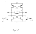
- FIG 6A is a block diagram illustrating an electrically coupled phase synchronous LC tank oscillator.
- Each oscillator stage, 602, 604, 606, and 608 includes a pair of inputs and a pair of outputs.
- a preferred design for each oscillator stage is shown in Figure 7 .
- Each output is connected to an input of the next oscillator in the chain. This configuration results in each of the oscillators oscillating in a synchronous manner.
- FIG. 6B is a block diagram illustrating an alternate design for an electrically coupled phase synchronous oscillator.
- Each oscillator stage, 612, 614, 616, and 618 includes a pair of inputs and a pair of outputs.
- a preferred design for each of the LC tank oscillators is shown in Figure 7 .
- Each output is connected to an input of the next oscillator in the chain, with a different input selected than the input selected in Figure 1 . This configuration results in each of the oscillators oscillating in a synchronous manner.
- FIG. 6C is a diagram illustrating another LC tank oscillator architecture that utilizes four oscillator stages, 622, 624, 626, and 628 that oscillate synchronously.
- Each oscillator stage includes four inputs and two outputs. The inputs and outputs are again configured to cause the oscillator stages to oscillate in phase.
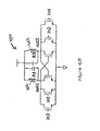
- FIG. 7 is a diagram illustrating an LC tank oscillator.
- LC tank oscillator 700 includes input node 702 and input node 704. The input nodes are coupled to the LC portion of the circuit 706 via a network of transistors. Because the individual LC tank oscillators oscillate synchronously, the inductors may be configured in a mutually inductive manner. Each inductor is laid out so that the area in which its flux is contained substantially coexists with the flux area of the other inductors that comprise the other oscillators in the ring.
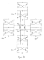
- Figure 8A is a diagram illustrating a rectangular physical layout for 4 inductors that are mutually inductive in the manner described above.
- the layout includes inductors 802, 804, 806 and 808.
- the layout is symmetric and the flux area of the inductors substantially overlaps. Dashed lines are used to illustrate when one inductor wire drops to a lower layer to pass under another inductor wire.
- This layout is implemented using a multilayer metal structure as described in Figure 8D . Each conductor that forms a loop begins at a first upper layer, then transitions to a second lower layer to pass under another inductor when that is required and then transitions back to the first layer.
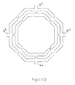
- Figure 8B is a diagram illustrating an octagonal physical layout for 4 inductors that are mutually inductive in the manner described above.
- the layout includes inductors 812, 814, 816 and 818.
- the layout is symmetric and the flux area of the inductors substantially overlaps. Dashed lines are used to illustrate when one line passes under another line.
- This layout is implemented using a multilayer metal structure as described in Figure 8D .
- the octagonal layout shown has the advantage that the angle of the turns is less acute, which reduces current crowding.
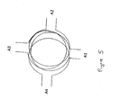
- Figure 8C is a diagram illustrating a circular layout for 4 inductors that are mutually inductive in the manner described above.
- the layout includes inductors 822, 824, 826 and 828.
- the layout is symmetric and the flux area of the inductors substantially overlaps. Dashed lines are used to illustrate when one line passes under another line.
- This layout is implemented using a multilayer metal structure as described in Figure 8D .
- the circular layout shown has the advantage eliminating the angular turns, which reduces current crowding.
- Figure 8D is a diagram illustrating in detail how one inductor passes below another inductor at a crossing point.
- the inductors are laid out on a top metal layer.
- the top metal layer may be thicker (on the order of two or three times thicker in some embodiments) than the second layer that is just below the top layer.
- the lower layers tend to have higher resistance. This problem can be ameliorated by connecting the top layer to two or more lower layers in parallel.
- one inductor is interrupted in the top layer and is connected to one or more lower layers using one or more vias. Once the crossing point has passed, the inductor resumes on the top layer and one or more vias connect the lower layers to the top layer.
- inductor 850 is disposed in the top layer until a crossing point with inductor 860 is reached.
- Inductor 850 is interrupted in the top layer and is connected to the second layer and the third layer by via 851.
- Second layer portion 852 and third layer portion 854 of inductor 850 run below inductor 860.
- via 855 connects second layer portion 852 and third layer portion 854 back to the top layer and inductor 850 resumes on the top layer.
- different numbers of layers may be used. In general, only 2 layers are required, but additional layers may be used to lower the resistance of the portion of the inductor that drops down to a lower layer.
- Figure 9A is a diagram illustrating a 2 oscillator stage synchronous LC tank oscillator where the oscillators are inductively coupled without electrical coupling.
- Oscillator 902 and oscillator 904 are inductively coupled through their inductors 903 and 905.
- Each of the inductors includes a center tap that is connected to a bias voltage Vdd.
- the inductive coupling causes the oscillator stages to oscillate synchronously without electrical coupling. By replacing electrical coupling with inductive coupling, the noise associated with the electrical coupling circuit is eliminated.
- Figure 9B is a diagram illustrating a layout for 2 inductors that are mutually inductive in the manner described above.
- the inductors are laid out on a top layer with inductor 914 dropping down to a lower layer in order to cross under inductor 912 at the appropriate point.
- Each inductor includes a center tap.
- the area in which the magnetic flux is contained for each inductor substantially coexists with the flux area of the other inductor.
- different shaped inductors are used, such as the hexagonal shape and circular shape shown above.
- Figure 9C is a diagram illustrating a 4 oscillator stage synchronous LC tank oscillator where the oscillators are inductively coupled without electrical coupling.
- Oscillators 932, 934, 936, and 938 are inductively coupled through their inductors 942, 944, 946, and 948.
- the inductors are disposed in a manner as shown in Figures 8A-8C so that the areas in which flux is contained substantially overlap.
- the inductive coupling causes the oscillator stages to oscillate synchronously without electrical coupling. By replacing electrical coupling with inductive coupling, the noise associated with the electrical coupling circuit is eliminated.
- FIG 10 is a diagram illustrating a 4 oscillator stage synchronous LC tank oscillator where the oscillators are inductively coupled with electrical coupling selectively included and controlled by a set of switches. Electrical coupling is selectively connected or disconnected using the switches.
- Oscillators 952, 954, 936, and 938 are inductively coupled through their inductors 962, 964, 966, and 968.
- Switches 971, 972, 973, 975, 976, 977, and 978 selectively connect or disconnect electrical coupling among the oscillators.
- the inductors are disposed in a manner as shown in Figures 8A-8C so that the areas in which flux is contained substantially overlap.
- the inductive coupling causes the oscillator stages to oscillate synchronously without electrical coupling.
- the noise associated with the electrical coupling circuit is eliminated.
- a number of embodiments of LC tank oscillators have been described that include coupled inductors.
- two or more oscillators are synchronized using inductive coupling without electrical coupling or with reduced electrical coupling.
- the synchronous coupling improves the phase noise of the oscillators.
- the inductive coupling increases the Q, which improves the phase noise. Lower phase noise for the same power or lower power for the same phase noise is achieved compared to non-synchronous oscillators.
- the coupled inductors occupy less area since they overlap.
Landscapes
- Engineering & Computer Science (AREA)
- Power Engineering (AREA)
- Inductance-Capacitance Distribution Constants And Capacitance-Resistance Oscillators (AREA)
Claims (22)
- Phasensynchroner Mehrfach-LC-Tank-Oszillator, der Folgendes umfasst:eine Vielzahl von Oszillatorstufen (952, 954, 936, 938), wobei die Oszillatorstufen so konfiguriert sind, dass sie synchron schwingen, wobei die Phase von jeder der Vielzahl von Oszillatorstufen im Wesentlichen gleich ist, undwobei die Vielzahl von Oszillatorstufen (952, 954, 936, 938) induktiv gekoppelt ist, wobei eine erste Induktionsspule (850, 962) und eine zweite Induktionsspule (860, 964) auf einer oberen Schicht eines integrierten Schaltkreises angeordnet sind,
dadurch gekennzeichnet, dass an einem Kreuzungspunkt mit der zweiten Induktionsspule (860) ein Teil der ersten Induktionsspule (850) auf mindestens einer Schicht (852) unter der oberen Schicht angeordnet ist und der Abschnitt der ersten Induktionsspule nach dem Kreuzungspunkt zu der oberen Schicht zurückkehrt. - Phasensynchroner Mehrfach-LC-Tank-Oszillator nach Anspruch 1, wobei die synchrone Schwingung im Wesentlichen durch magnetische Kopplung verursacht wird.
- Phasensynchroner Mehrfach-LC-Tank-Oszillator nach Anspruch 1, wobei die Stufen (952, 954, 936, 938) des synchronen Oszillators nicht im Wesentlichen elektrisch gekoppelt sind.
- Phasensynchroner Mehrfach-LC-Tank-Oszillator nach Anspruch 1, wobei die Stufen (952, 954, 936, 938) des synchronen Oszillators während eines ersten Zeitraums elektrisch gekoppelt sind und die elektrische Kopplung während eines zweiten Zeitraums getrennt ist.
- Phasensynchroner Mehrfach-LC-Tank-Oszillator nach Anspruch 1, wobei die Stufen (952, 954, 936, 938) des synchronen Oszillators während eines ersten Zeitraums elektrisch gekoppelt sind und die elektrische Kopplung während eines zweiten Zeitraums verringert ist.
- Phasensynchroner Mehrfach-LC-Tank-Oszillator nach Anspruch 1, wobei die Vielzahl der Oszillatorstufen (952, 954, 936, 938) vier Oszillatorstufen umfasst.
- Phasensynchroner Mehrfach-LC-Tank-Oszillator nach Anspruch 1, wobei die Vielzahl der Oszillatorstufen (952, 954, 936, 938) zwei Oszillatorstufen umfasst.
- Phasensynchroner Mehrfach-LC-Tank-Oszillator nach Anspruch 1, wobei die induktive Kopplung unter Verwendung von zwei Mittelabgriffsinduktionsspulen erzielt wird.
- Phasensynchroner Mehrfach-LC-Tank-Oszillator nach Anspruch 1, wobei die induktive Kopplung unter Verwendung von Induktionsspulen erzielt wird, die gegenseitig induktiv sind.
- Phasensynchroner Mehrfach-LC-Tank-Oszillator nach Anspruch 1, wobei die induktive Kopplung unter Verwendung von Induktionsspulen erzielt wird, die Bereiche aufweisen, in denen Fluss enthalten ist und die im Wesentlichen nebeneinander bestehen.
- Phasensynchroner Mehrfach-LC-Tank-Oszillator nach Anspruch 1, wobei mindestens eine der Oszillatorstufen (952, 954, 936, 938) einen Schalter (971, 972, 973, 975, 976, 977, 978) umfasst.
- Phasensynchroner Mehrfach-LC-Tank-Oszillator nach Anspruch 1, wobei der phasensynchrone Mehrfach-LC-Tank-Oszillator in einem drahtlosen Sender-Empfänger verwendet wird.
- Mehrfach-LC-Tank-Oszillator nach Anspruch 9, wobei die erste Induktionsspule und die zweite Induktionsspule so angeordnet sind, dass die Flussbereiche, die von den Induktionsspulen umgeben sind, überlappen.
- Mehrfach-LC-Tank-Oszillator nach Anspruch 9, wobei die erste Induktionsspule und die zweite Induktionsspule auf drei Schichten eines integrierten Schaltkreises angeordnet sind.
- Mehrfach-LC-Tank-Oszillator nach Anspruch 9, wobei der Abschnitt der ersten Induktionsspule auf mindestens zwei Schichten angeordnet ist, die sich unterhalb einer Schicht befinden, die die zweite Induktionsspule umfasst.
- Mehrfach-LC-Tank-Oszillator nach Anspruch 9, wobei die erste Induktionsspule und die zweite Induktionsspule jeweils in einer hexagonalen Form angeordnet sind.
- Mehrfach-LC-Tank-Oszillator nach Anspruch 9, wobei die erste Induktionsspule und die zweite Induktionsspule jeweils in einer Kreisform angeordnet sind.
- Mehrfach-LC-Tank-Oszillator nach Anspruch 9, wobei die erste Induktionsspule auf eine zweite Schicht absinkt, wenn sich die erste Induktionsspule und die zweite Induktionsspule kreuzen.
- Mehrfach-LC-Tank-Oszillator nach Anspruch 9, wobei die erste Induktionsspule und die zweite Induktionsspule auf höchstens zwei Schichten eines integrierten Schaltkreises angeordnet sind.
- Mehrfach-LC-Tank-Oszillator nach Anspruch 9, der ferner Folgendes umfasst:eine dritte Oszillatorstufe (956) mit einer dritten Induktionsspule (966) und eine vierte Oszillatorstufe (958) mit einer vierten Induktionsspule (968), wobei die erste Induktionsspule, die zweite Induktionsspule, die dritte Induktionsspule und die vierte Induktionsspule alle gegenseitig induktiv sind.
- Mehrfach-LC-Tank-Oszillator nach Anspruch 9, der ferner Folgendes umfasst:eine dritte Oszillatorstufe mit einer dritten Induktionsspule und eine vierte Oszillatorstufe mit einer vierten Induktionsspule, wobei die erste Induktionsspule, die zweite Induktionsspule, die dritte Induktionsspule und die vierte Induktionsspule alle gegenseitig induktiv sind und wobei die eine der Induktionsspulen auf eine zweite Schicht absinkt, wenn sich zwei der Induktionsspulen kreuzen.
- Mehrfach-LC-Tank-Oszillator nach Anspruch 9, der ferner Folgendes umfasst:eine dritte Oszillatorstufe mit einer dritten Induktionsspule und eine vierte Oszillatorstufe mit einer vierten Induktionsspule, wobei die erste Induktionsspule, die zweite Induktionsspule, die dritte Induktionsspule und die vierte Induktionsspule alle gegenseitig induktiv sind und wobei die erste Induktionsspule und die zweite Induktionsspule, die dritte Induktionsspule und die vierte Induktionsspule auf zwei Schichten eines integrierten Schaltkreises angeordnet sind und wobei die erste Induktionsspule und die zweite Induktionsspule auf einer oberen Schicht des integrierten Schaltkreises angeordnet sind.
Applications Claiming Priority (5)
| Application Number | Priority Date | Filing Date | Title |
|---|---|---|---|
| US101560 | 1993-08-02 | ||
| US4521 | 1998-01-08 | ||
| US10/004,521 US6900699B1 (en) | 2001-11-14 | 2001-11-14 | Phase synchronous multiple LC tank oscillator |
| US10/101,560 US7005930B1 (en) | 2001-11-14 | 2002-03-18 | Synchronously coupled oscillator |
| PCT/US2002/036823 WO2003043175A1 (en) | 2001-11-14 | 2002-11-14 | Low noise oscillator |
Publications (3)
| Publication Number | Publication Date |
|---|---|
| EP1456940A1 EP1456940A1 (de) | 2004-09-15 |
| EP1456940A4 EP1456940A4 (de) | 2005-12-07 |
| EP1456940B1 true EP1456940B1 (de) | 2013-12-18 |
Family
ID=26673112
Family Applications (1)
| Application Number | Title | Priority Date | Filing Date |
|---|---|---|---|
| EP02789700.8A Expired - Lifetime EP1456940B1 (de) | 2001-11-14 | 2002-11-14 | Rauscharmer oszillator |
Country Status (4)
| Country | Link |
|---|---|
| US (2) | US7005930B1 (de) |
| EP (1) | EP1456940B1 (de) |
| CN (1) | CN100440724C (de) |
| WO (1) | WO2003043175A1 (de) |
Families Citing this family (40)
| Publication number | Priority date | Publication date | Assignee | Title |
|---|---|---|---|---|
| US7764130B2 (en) | 1999-01-22 | 2010-07-27 | Multigig Inc. | Electronic circuitry |
| ATE400923T1 (de) | 2000-05-11 | 2008-07-15 | Multigig Ltd | Elektronischer pulserzeuger und oszillator |
| JP2005303839A (ja) * | 2004-04-14 | 2005-10-27 | Matsushita Electric Ind Co Ltd | 電圧制御発振装置 |
| EP1608063A3 (de) * | 2004-06-17 | 2006-09-13 | STMicroelectronics S.r.l. | Phasenschieber-Kopplungstechnik für mehrphasige Ringoszillatoren mit LC-Schwingkreis |
| US7250826B2 (en) | 2005-07-19 | 2007-07-31 | Lctank Llc | Mutual inductance in transformer based tank circuitry |
| US7511588B2 (en) * | 2005-07-19 | 2009-03-31 | Lctank Llc | Flux linked LC tank circuits forming distributed clock networks |
| US7508280B2 (en) * | 2005-07-19 | 2009-03-24 | Lc Tank Llc | Frequency adjustment techniques in coupled LC tank circuits |
| US7786836B2 (en) * | 2005-07-19 | 2010-08-31 | Lctank Llc | Fabrication of inductors in transformer based tank circuitry |
| US8022776B2 (en) * | 2005-08-04 | 2011-09-20 | The Regents Of The University Of California | Origami cascaded topology for analog and mixed-signal applications |
| TW200822528A (en) * | 2006-11-07 | 2008-05-16 | Univ Nat Taiwan Science Tech | Multi-phase voltage-control osillator |
| WO2008121857A1 (en) | 2007-03-29 | 2008-10-09 | Multigig Inc. | Wave reversing system and method for a rotary traveling wave oscillator |
| US8913978B2 (en) * | 2007-04-09 | 2014-12-16 | Analog Devices, Inc. | RTWO-based down converter |
| DE102007023795A1 (de) * | 2007-05-21 | 2008-12-04 | Atmel Duisburg Gmbh | Oszillator zum Erzeugen von unterschiedlichen Schwingungen |
| EP2201676B1 (de) * | 2007-10-23 | 2014-06-04 | Telefonaktiebolaget LM Ericsson (publ) | Zweibandgekoppelter vco |
| US8742857B2 (en) | 2008-05-15 | 2014-06-03 | Analog Devices, Inc. | Inductance enhanced rotary traveling wave oscillator circuit and method |
| JP4922369B2 (ja) * | 2009-08-28 | 2012-04-25 | 株式会社東芝 | 電圧制御発振器 |
| US7961056B2 (en) * | 2009-09-10 | 2011-06-14 | Intel Corporation | Low phase noise voltage controlled oscillator |
| US8576019B2 (en) | 2011-04-22 | 2013-11-05 | Continental Automotive Systems, Inc | Synchronized array power oscillator with leg inductors |
| US9275784B2 (en) | 2011-09-23 | 2016-03-01 | Rambus Inc. | Electronic circuits using coupled multi-inductors |
| US8487710B2 (en) | 2011-12-12 | 2013-07-16 | Analog Devices, Inc. | RTWO-based pulse width modulator |
| US8581668B2 (en) | 2011-12-20 | 2013-11-12 | Analog Devices, Inc. | Oscillator regeneration device |
| EP2648193B1 (de) | 2012-04-03 | 2015-07-29 | Telefonaktiebolaget L M Ericsson (publ) | Induktor-Layout, und spannungsgesteuertes Oszillator- (VCO) -System |
| US9306614B2 (en) | 2013-03-26 | 2016-04-05 | Stmicroelectronics S.R.L. | Power oscillator apparatus with transformer-based power combining for galvanically-isolated bidirectional data communication and power transfer |
| US9240752B2 (en) | 2013-03-26 | 2016-01-19 | Stmicroelectronics S.R.L. | Power oscillator apparatus with transformer-based power combining |
| EP3220419B1 (de) | 2013-10-16 | 2020-07-08 | Telefonaktiebolaget LM Ericsson (publ) | Sende-empfänger, empfänger und kommunikationsvorrichtung mit schalteranordnung |
| DK2863429T3 (en) | 2013-10-16 | 2017-09-04 | ERICSSON TELEFON AB L M (publ) | Adjustable inductor device, transceiver, method and computer program |
| US9306603B2 (en) | 2014-01-24 | 2016-04-05 | Qualcomm Incorporated | Tunable radio frequency (RF) front-end architecture using filter having adjustable inductance and capacitance |
| US9356608B1 (en) | 2014-04-29 | 2016-05-31 | Microsemi Storage Solutions (U.S.), Inc. | Method and apparatus for controlling mismatch in a voltage controlled oscillator array |
| US9819307B2 (en) * | 2015-06-19 | 2017-11-14 | Qualcomm Incorporated | Low power current re-using transformer-based dual-band voltage controlled oscillator |
| US9735732B1 (en) * | 2016-06-09 | 2017-08-15 | International Business Machines Corporation | Coupled oscillators |
| US10389301B2 (en) | 2016-10-04 | 2019-08-20 | Microsemi Solutions (U.S.), Inc. | Method and apparatus for reconfigurable multicore oscillator |
| US10277233B2 (en) | 2016-10-07 | 2019-04-30 | Analog Devices, Inc. | Apparatus and methods for frequency tuning of rotary traveling wave oscillators |
| US10312922B2 (en) | 2016-10-07 | 2019-06-04 | Analog Devices, Inc. | Apparatus and methods for rotary traveling wave oscillators |
| US10903823B2 (en) | 2018-09-29 | 2021-01-26 | Qualcomm Incorporated | Oscillation signal production |
| US11527992B2 (en) | 2019-09-19 | 2022-12-13 | Analog Devices International Unlimited Company | Rotary traveling wave oscillators with distributed stubs |
| US11264949B2 (en) | 2020-06-10 | 2022-03-01 | Analog Devices International Unlimited Company | Apparatus and methods for rotary traveling wave oscillators |
| CN112003569B (zh) * | 2020-09-07 | 2021-10-15 | 华南理工大学 | 一种基于三电感耦合的高稳定超宽带调谐压控振荡器 |
| US11539353B2 (en) | 2021-02-02 | 2022-12-27 | Analog Devices International Unlimited Company | RTWO-based frequency multiplier |
| US11901863B2 (en) | 2022-04-28 | 2024-02-13 | Stmicroelectronics S.R.L. | Capacitively-coupled stacked class-D oscillators for galvanic isolation |
| US11621670B1 (en) | 2022-04-28 | 2023-04-04 | Stmicroelectronics S.R.L. | Capacitively-coupled stacked class-d oscillators for galvanic isolation |
Citations (2)
| Publication number | Priority date | Publication date | Assignee | Title |
|---|---|---|---|---|
| US4940939A (en) * | 1989-01-09 | 1990-07-10 | Khait Alexandr L | Apparatus with inductive loop synchronized oscillators for measuring the magnetic content of non-metallic samples |
| US5912596A (en) * | 1998-01-26 | 1999-06-15 | International Business Machines Corporation | Apparatus and method for frequency tuning an LC oscillator in a integrated clock circuit |
Family Cites Families (19)
| Publication number | Priority date | Publication date | Assignee | Title |
|---|---|---|---|---|
| GB1132721A (en) * | 1965-02-05 | 1968-11-06 | Atomic Energy Authority Uk | Variable frequency oscillators |
| US3731230A (en) | 1971-12-17 | 1973-05-01 | Motorola Inc | Broadband circuit for minimizing the effects of crystal shunt capacitance |
| US4574936A (en) * | 1983-05-10 | 1986-03-11 | Lance Klinger | Coin accepter/rejector including symmetrical dual feedback oscillator |
| GB9308944D0 (en) | 1993-04-30 | 1993-06-16 | Inmos Ltd | Ring oscillator |
| US5396195A (en) * | 1993-12-13 | 1995-03-07 | At&T Corp. | Low-power-dissipation CMOS oscillator circuits |
| US5561399A (en) | 1995-04-19 | 1996-10-01 | Telefonaktiebolaget Lm Ericsson | Cascaded multi-resonator oscillator having high Q-value |
| US5561398A (en) * | 1995-05-16 | 1996-10-01 | National Semiconductor Corporation | LC-tuned voltage controlled ring oscillator |
| JP3149797B2 (ja) | 1996-09-18 | 2001-03-26 | 日本電気株式会社 | 電圧制御発振回路 |
| US5892425A (en) | 1997-04-10 | 1999-04-06 | Virginia Tech Intellectual Properties, Inc. | Interwound center-tapped spiral inductor |
| US6232847B1 (en) | 1997-04-28 | 2001-05-15 | Rockwell Science Center, Llc | Trimmable singleband and tunable multiband integrated oscillator using micro-electromechanical system (MEMS) technology |
| US6104253A (en) | 1997-05-21 | 2000-08-15 | North Carolina State University | Integrated circuits having cooperative ring oscillator clock circuits therein to minimize clock skew |
| DE19738841A1 (de) | 1997-09-05 | 1999-03-11 | Hella Kg Hueck & Co | Induktiver Winkelsensor |
| KR19990025790A (ko) | 1997-09-18 | 1999-04-06 | 이계철 | 다중궤환 루프 링발진기 및 그 지연셀 |
| KR100278551B1 (ko) | 1997-10-29 | 2001-01-15 | 김범섭 | 고주파 저잡음 발진장치 |
| KR100268050B1 (ko) | 1997-12-02 | 2000-11-01 | 김범섭 | 딜레이 쎌 및 이를 이용한 가변주파수 링 발진회로 |
| NL1012710C2 (nl) * | 1999-07-26 | 2001-01-29 | Spronck Josephus Wilhelmus Spronck | Werkwijze voor het vergelijken van, of het meten van de verschillen tussen, twee of meer elektrische impedanties. |
| JP3480384B2 (ja) | 1999-09-10 | 2003-12-15 | 株式会社村田製作所 | 積層型lc共振器および積層型lcフィルタ |
| US6417740B1 (en) * | 2001-02-22 | 2002-07-09 | Chartered Semiconductor Manufacturing Ltd. | Wide-band/multi-band voltage controlled oscillator |
| US6717478B1 (en) | 2001-04-09 | 2004-04-06 | Silicon Image | Multi-phase voltage controlled oscillator (VCO) with common mode control |
-
2002
- 2002-03-18 US US10/101,560 patent/US7005930B1/en not_active Expired - Lifetime
- 2002-11-14 WO PCT/US2002/036823 patent/WO2003043175A1/en not_active Ceased
- 2002-11-14 EP EP02789700.8A patent/EP1456940B1/de not_active Expired - Lifetime
- 2002-11-14 CN CNB02827041XA patent/CN100440724C/zh not_active Expired - Fee Related
-
2005
- 2005-12-12 US US11/301,859 patent/US7295076B2/en not_active Expired - Lifetime
Patent Citations (2)
| Publication number | Priority date | Publication date | Assignee | Title |
|---|---|---|---|---|
| US4940939A (en) * | 1989-01-09 | 1990-07-10 | Khait Alexandr L | Apparatus with inductive loop synchronized oscillators for measuring the magnetic content of non-metallic samples |
| US5912596A (en) * | 1998-01-26 | 1999-06-15 | International Business Machines Corporation | Apparatus and method for frequency tuning an LC oscillator in a integrated clock circuit |
Also Published As
| Publication number | Publication date |
|---|---|
| EP1456940A1 (de) | 2004-09-15 |
| EP1456940A4 (de) | 2005-12-07 |
| US7005930B1 (en) | 2006-02-28 |
| US7295076B2 (en) | 2007-11-13 |
| CN1613175A (zh) | 2005-05-04 |
| CN100440724C (zh) | 2008-12-03 |
| WO2003043175A1 (en) | 2003-05-22 |
| US20060091966A1 (en) | 2006-05-04 |
Similar Documents
| Publication | Publication Date | Title |
|---|---|---|
| EP1456940B1 (de) | Rauscharmer oszillator | |
| RU2416132C2 (ru) | Катушка переменной индуктивности в интегральном исполнении | |
| US20220360219A1 (en) | Radio frequency oscillator | |
| US8810322B2 (en) | Apparatus and method for frequency generation | |
| EP2769466B1 (de) | Spannungsgesteuerte oszillatoren mit niedrigem phasenrauschen | |
| US8717138B2 (en) | Inductor combining primary and secondary coils with phase shifting | |
| US7164323B1 (en) | Phase synchronous multiple LC tank oscillator | |
| US9899991B2 (en) | Circuits and methods of synchronizing differential ring-type oscillators | |
| EP1378054A1 (de) | Oszillator mit verbesserter magnetkopplungsunterdrückung | |
| US10164570B2 (en) | Coupling structure for inductive device | |
| US10658975B2 (en) | Semiconductor device and method | |
| US20130076359A1 (en) | Output stage module for a power amplifier device | |
| CN105450955B (zh) | 用于可切换地路由下变频rf信号的设备和方法 | |
| EP1318530B1 (de) | Induktives Bauelement mit hohem Gütefaktor | |
| HK1120654B (en) | Variable integrated inductor |
Legal Events
| Date | Code | Title | Description |
|---|---|---|---|
| PUAI | Public reference made under article 153(3) epc to a published international application that has entered the european phase |
Free format text: ORIGINAL CODE: 0009012 |
|
| 17P | Request for examination filed |
Effective date: 20040519 |
|
| AK | Designated contracting states |
Kind code of ref document: A1 Designated state(s): AT BE BG CH CY CZ DE DK EE ES FI FR GB GR IE IT LI LU MC NL PT SE SK TR |
|
| AX | Request for extension of the european patent |
Extension state: AL LT LV MK RO SI |
|
| A4 | Supplementary search report drawn up and despatched |
Effective date: 20051026 |
|
| 17Q | First examination report despatched |
Effective date: 20071217 |
|
| RAP1 | Party data changed (applicant data changed or rights of an application transferred) |
Owner name: QUALCOMM INCORPORATED |
|
| GRAP | Despatch of communication of intention to grant a patent |
Free format text: ORIGINAL CODE: EPIDOSNIGR1 |
|
| INTG | Intention to grant announced |
Effective date: 20130610 |
|
| GRAS | Grant fee paid |
Free format text: ORIGINAL CODE: EPIDOSNIGR3 |
|
| GRAA | (expected) grant |
Free format text: ORIGINAL CODE: 0009210 |
|
| AK | Designated contracting states |
Kind code of ref document: B1 Designated state(s): AT BE BG CH CY CZ DE DK EE ES FI FR GB GR IE IT LI LU MC NL PT SE SK TR |
|
| REG | Reference to a national code |
Ref country code: GB Ref legal event code: FG4D |
|
| REG | Reference to a national code |
Ref country code: CH Ref legal event code: EP |
|
| REG | Reference to a national code |
Ref country code: AT Ref legal event code: REF Ref document number: 645980 Country of ref document: AT Kind code of ref document: T Effective date: 20140115 |
|
| REG | Reference to a national code |
Ref country code: IE Ref legal event code: FG4D |
|
| REG | Reference to a national code |
Ref country code: DE Ref legal event code: R096 Ref document number: 60245869 Country of ref document: DE Effective date: 20140206 |
|
| REG | Reference to a national code |
Ref country code: NL Ref legal event code: VDEP Effective date: 20131218 |
|
| PG25 | Lapsed in a contracting state [announced via postgrant information from national office to epo] |
Ref country code: SE Free format text: LAPSE BECAUSE OF FAILURE TO SUBMIT A TRANSLATION OF THE DESCRIPTION OR TO PAY THE FEE WITHIN THE PRESCRIBED TIME-LIMIT Effective date: 20131218 Ref country code: FI Free format text: LAPSE BECAUSE OF FAILURE TO SUBMIT A TRANSLATION OF THE DESCRIPTION OR TO PAY THE FEE WITHIN THE PRESCRIBED TIME-LIMIT Effective date: 20131218 |
|
| REG | Reference to a national code |
Ref country code: AT Ref legal event code: MK05 Ref document number: 645980 Country of ref document: AT Kind code of ref document: T Effective date: 20131218 |
|
| PG25 | Lapsed in a contracting state [announced via postgrant information from national office to epo] |
Ref country code: BE Free format text: LAPSE BECAUSE OF FAILURE TO SUBMIT A TRANSLATION OF THE DESCRIPTION OR TO PAY THE FEE WITHIN THE PRESCRIBED TIME-LIMIT Effective date: 20131218 Ref country code: EE Free format text: LAPSE BECAUSE OF FAILURE TO SUBMIT A TRANSLATION OF THE DESCRIPTION OR TO PAY THE FEE WITHIN THE PRESCRIBED TIME-LIMIT Effective date: 20131218 |
|
| PG25 | Lapsed in a contracting state [announced via postgrant information from national office to epo] |
Ref country code: SK Free format text: LAPSE BECAUSE OF FAILURE TO SUBMIT A TRANSLATION OF THE DESCRIPTION OR TO PAY THE FEE WITHIN THE PRESCRIBED TIME-LIMIT Effective date: 20131218 Ref country code: ES Free format text: LAPSE BECAUSE OF FAILURE TO SUBMIT A TRANSLATION OF THE DESCRIPTION OR TO PAY THE FEE WITHIN THE PRESCRIBED TIME-LIMIT Effective date: 20131218 Ref country code: CZ Free format text: LAPSE BECAUSE OF FAILURE TO SUBMIT A TRANSLATION OF THE DESCRIPTION OR TO PAY THE FEE WITHIN THE PRESCRIBED TIME-LIMIT Effective date: 20131218 Ref country code: AT Free format text: LAPSE BECAUSE OF FAILURE TO SUBMIT A TRANSLATION OF THE DESCRIPTION OR TO PAY THE FEE WITHIN THE PRESCRIBED TIME-LIMIT Effective date: 20131218 Ref country code: CY Free format text: LAPSE BECAUSE OF FAILURE TO SUBMIT A TRANSLATION OF THE DESCRIPTION OR TO PAY THE FEE WITHIN THE PRESCRIBED TIME-LIMIT Effective date: 20131218 Ref country code: PT Free format text: LAPSE BECAUSE OF FAILURE TO SUBMIT A TRANSLATION OF THE DESCRIPTION OR TO PAY THE FEE WITHIN THE PRESCRIBED TIME-LIMIT Effective date: 20140418 Ref country code: NL Free format text: LAPSE BECAUSE OF FAILURE TO SUBMIT A TRANSLATION OF THE DESCRIPTION OR TO PAY THE FEE WITHIN THE PRESCRIBED TIME-LIMIT Effective date: 20131218 |
|
| REG | Reference to a national code |
Ref country code: DE Ref legal event code: R097 Ref document number: 60245869 Country of ref document: DE |
|
| PLBE | No opposition filed within time limit |
Free format text: ORIGINAL CODE: 0009261 |
|
| STAA | Information on the status of an ep patent application or granted ep patent |
Free format text: STATUS: NO OPPOSITION FILED WITHIN TIME LIMIT |
|
| PG25 | Lapsed in a contracting state [announced via postgrant information from national office to epo] |
Ref country code: DK Free format text: LAPSE BECAUSE OF FAILURE TO SUBMIT A TRANSLATION OF THE DESCRIPTION OR TO PAY THE FEE WITHIN THE PRESCRIBED TIME-LIMIT Effective date: 20131218 |
|
| 26N | No opposition filed |
Effective date: 20140919 |
|
| REG | Reference to a national code |
Ref country code: DE Ref legal event code: R097 Ref document number: 60245869 Country of ref document: DE Effective date: 20140919 |
|
| PG25 | Lapsed in a contracting state [announced via postgrant information from national office to epo] |
Ref country code: LU Free format text: LAPSE BECAUSE OF FAILURE TO SUBMIT A TRANSLATION OF THE DESCRIPTION OR TO PAY THE FEE WITHIN THE PRESCRIBED TIME-LIMIT Effective date: 20141114 Ref country code: MC Free format text: LAPSE BECAUSE OF FAILURE TO SUBMIT A TRANSLATION OF THE DESCRIPTION OR TO PAY THE FEE WITHIN THE PRESCRIBED TIME-LIMIT Effective date: 20131218 |
|
| REG | Reference to a national code |
Ref country code: CH Ref legal event code: PL |
|
| PG25 | Lapsed in a contracting state [announced via postgrant information from national office to epo] |
Ref country code: LI Free format text: LAPSE BECAUSE OF NON-PAYMENT OF DUE FEES Effective date: 20141130 Ref country code: CH Free format text: LAPSE BECAUSE OF NON-PAYMENT OF DUE FEES Effective date: 20141130 |
|
| REG | Reference to a national code |
Ref country code: IE Ref legal event code: MM4A |
|
| REG | Reference to a national code |
Ref country code: FR Ref legal event code: ST Effective date: 20150731 |
|
| PG25 | Lapsed in a contracting state [announced via postgrant information from national office to epo] |
Ref country code: IE Free format text: LAPSE BECAUSE OF NON-PAYMENT OF DUE FEES Effective date: 20141114 |
|
| PG25 | Lapsed in a contracting state [announced via postgrant information from national office to epo] |
Ref country code: FR Free format text: LAPSE BECAUSE OF NON-PAYMENT OF DUE FEES Effective date: 20141201 |
|
| PG25 | Lapsed in a contracting state [announced via postgrant information from national office to epo] |
Ref country code: BG Free format text: LAPSE BECAUSE OF FAILURE TO SUBMIT A TRANSLATION OF THE DESCRIPTION OR TO PAY THE FEE WITHIN THE PRESCRIBED TIME-LIMIT Effective date: 20131218 |
|
| PG25 | Lapsed in a contracting state [announced via postgrant information from national office to epo] |
Ref country code: GR Free format text: LAPSE BECAUSE OF FAILURE TO SUBMIT A TRANSLATION OF THE DESCRIPTION OR TO PAY THE FEE WITHIN THE PRESCRIBED TIME-LIMIT Effective date: 20140319 Ref country code: IT Free format text: LAPSE BECAUSE OF FAILURE TO SUBMIT A TRANSLATION OF THE DESCRIPTION OR TO PAY THE FEE WITHIN THE PRESCRIBED TIME-LIMIT Effective date: 20131218 |
|
| PG25 | Lapsed in a contracting state [announced via postgrant information from national office to epo] |
Ref country code: TR Free format text: LAPSE BECAUSE OF FAILURE TO SUBMIT A TRANSLATION OF THE DESCRIPTION OR TO PAY THE FEE WITHIN THE PRESCRIBED TIME-LIMIT Effective date: 20131218 |
|
| PGFP | Annual fee paid to national office [announced via postgrant information from national office to epo] |
Ref country code: DE Payment date: 20191017 Year of fee payment: 18 |
|
| PGFP | Annual fee paid to national office [announced via postgrant information from national office to epo] |
Ref country code: GB Payment date: 20191029 Year of fee payment: 18 |
|
| REG | Reference to a national code |
Ref country code: DE Ref legal event code: R119 Ref document number: 60245869 Country of ref document: DE |
|
| GBPC | Gb: european patent ceased through non-payment of renewal fee |
Effective date: 20201114 |
|
| PG25 | Lapsed in a contracting state [announced via postgrant information from national office to epo] |
Ref country code: DE Free format text: LAPSE BECAUSE OF NON-PAYMENT OF DUE FEES Effective date: 20210601 Ref country code: GB Free format text: LAPSE BECAUSE OF NON-PAYMENT OF DUE FEES Effective date: 20201114 |