EP1457828A2 - Supervision de points de focalisation dans un appareil de projection lithographique - Google Patents
Supervision de points de focalisation dans un appareil de projection lithographique Download PDFInfo
- Publication number
- EP1457828A2 EP1457828A2 EP04075692A EP04075692A EP1457828A2 EP 1457828 A2 EP1457828 A2 EP 1457828A2 EP 04075692 A EP04075692 A EP 04075692A EP 04075692 A EP04075692 A EP 04075692A EP 1457828 A2 EP1457828 A2 EP 1457828A2
- Authority
- EP
- European Patent Office
- Prior art keywords
- height map
- substrate
- height
- raw
- map
- Prior art date
- Legal status (The legal status is an assumption and is not a legal conclusion. Google has not performed a legal analysis and makes no representation as to the accuracy of the status listed.)
- Withdrawn
Links
- 238000012544 monitoring process Methods 0.000 title description 2
- 239000000758 substrate Substances 0.000 claims abstract description 139
- 238000004519 manufacturing process Methods 0.000 claims abstract description 8
- 238000005259 measurement Methods 0.000 claims description 26
- 238000000034 method Methods 0.000 claims description 20
- 230000005855 radiation Effects 0.000 claims description 20
- 238000003384 imaging method Methods 0.000 claims description 11
- 238000011109 contamination Methods 0.000 claims description 10
- 230000009471 action Effects 0.000 claims description 6
- 238000009499 grossing Methods 0.000 claims description 6
- 230000009897 systematic effect Effects 0.000 claims description 2
- 235000012431 wafers Nutrition 0.000 description 54
- 239000002245 particle Substances 0.000 description 7
- 238000001514 detection method Methods 0.000 description 6
- 230000008569 process Effects 0.000 description 6
- 238000012545 processing Methods 0.000 description 6
- 230000003287 optical effect Effects 0.000 description 5
- XUIMIQQOPSSXEZ-UHFFFAOYSA-N Silicon Chemical compound [Si] XUIMIQQOPSSXEZ-UHFFFAOYSA-N 0.000 description 3
- 230000015654 memory Effects 0.000 description 3
- 229910052710 silicon Inorganic materials 0.000 description 3
- 239000010703 silicon Substances 0.000 description 3
- 238000004364 calculation method Methods 0.000 description 2
- 230000001419 dependent effect Effects 0.000 description 2
- 238000010894 electron beam technology Methods 0.000 description 2
- 238000001914 filtration Methods 0.000 description 2
- 239000000463 material Substances 0.000 description 2
- 238000007493 shaping process Methods 0.000 description 2
- 238000012935 Averaging Methods 0.000 description 1
- 230000002159 abnormal effect Effects 0.000 description 1
- 238000004458 analytical method Methods 0.000 description 1
- 238000012512 characterization method Methods 0.000 description 1
- 239000011248 coating agent Substances 0.000 description 1
- 238000000576 coating method Methods 0.000 description 1
- 239000000356 contaminant Substances 0.000 description 1
- 230000002950 deficient Effects 0.000 description 1
- 230000001627 detrimental effect Effects 0.000 description 1
- 238000011161 development Methods 0.000 description 1
- 238000006073 displacement reaction Methods 0.000 description 1
- 238000009826 distribution Methods 0.000 description 1
- 230000005670 electromagnetic radiation Effects 0.000 description 1
- 238000005530 etching Methods 0.000 description 1
- 230000004907 flux Effects 0.000 description 1
- 238000005286 illumination Methods 0.000 description 1
- 230000001939 inductive effect Effects 0.000 description 1
- 238000007689 inspection Methods 0.000 description 1
- 238000005468 ion implantation Methods 0.000 description 1
- 238000010884 ion-beam technique Methods 0.000 description 1
- 150000002500 ions Chemical class 0.000 description 1
- 239000004973 liquid crystal related substance Substances 0.000 description 1
- 238000001459 lithography Methods 0.000 description 1
- 230000005381 magnetic domain Effects 0.000 description 1
- 238000013507 mapping Methods 0.000 description 1
- 239000003550 marker Substances 0.000 description 1
- 230000007246 mechanism Effects 0.000 description 1
- 238000001465 metallisation Methods 0.000 description 1
- 230000003647 oxidation Effects 0.000 description 1
- 238000007254 oxidation reaction Methods 0.000 description 1
- 238000005498 polishing Methods 0.000 description 1
- 230000037452 priming Effects 0.000 description 1
- 230000000246 remedial effect Effects 0.000 description 1
- 230000004044 response Effects 0.000 description 1
- 239000004065 semiconductor Substances 0.000 description 1
- 238000003860 storage Methods 0.000 description 1
- 239000010409 thin film Substances 0.000 description 1
- 238000012546 transfer Methods 0.000 description 1
Images
Classifications
-
- G—PHYSICS
- G03—PHOTOGRAPHY; CINEMATOGRAPHY; ANALOGOUS TECHNIQUES USING WAVES OTHER THAN OPTICAL WAVES; ELECTROGRAPHY; HOLOGRAPHY
- G03F—PHOTOMECHANICAL PRODUCTION OF TEXTURED OR PATTERNED SURFACES, e.g. FOR PRINTING, FOR PROCESSING OF SEMICONDUCTOR DEVICES; MATERIALS THEREFOR; ORIGINALS THEREFOR; APPARATUS SPECIALLY ADAPTED THEREFOR
- G03F7/00—Photomechanical, e.g. photolithographic, production of textured or patterned surfaces, e.g. printing surfaces; Materials therefor, e.g. comprising photoresists; Apparatus specially adapted therefor
- G03F7/70—Microphotolithographic exposure; Apparatus therefor
- G03F7/70483—Information management; Active and passive control; Testing; Wafer monitoring, e.g. pattern monitoring
- G03F7/70605—Workpiece metrology
- G03F7/70616—Monitoring the printed patterns
- G03F7/7065—Defects, e.g. optical inspection of patterned layer for defects
-
- G—PHYSICS
- G03—PHOTOGRAPHY; CINEMATOGRAPHY; ANALOGOUS TECHNIQUES USING WAVES OTHER THAN OPTICAL WAVES; ELECTROGRAPHY; HOLOGRAPHY
- G03F—PHOTOMECHANICAL PRODUCTION OF TEXTURED OR PATTERNED SURFACES, e.g. FOR PRINTING, FOR PROCESSING OF SEMICONDUCTOR DEVICES; MATERIALS THEREFOR; ORIGINALS THEREFOR; APPARATUS SPECIALLY ADAPTED THEREFOR
- G03F9/00—Registration or positioning of originals, masks, frames, photographic sheets or textured or patterned surfaces, e.g. automatically
- G03F9/70—Registration or positioning of originals, masks, frames, photographic sheets or textured or patterned surfaces, e.g. automatically for microlithography
- G03F9/7003—Alignment type or strategy, e.g. leveling, global alignment
-
- G—PHYSICS
- G03—PHOTOGRAPHY; CINEMATOGRAPHY; ANALOGOUS TECHNIQUES USING WAVES OTHER THAN OPTICAL WAVES; ELECTROGRAPHY; HOLOGRAPHY
- G03F—PHOTOMECHANICAL PRODUCTION OF TEXTURED OR PATTERNED SURFACES, e.g. FOR PRINTING, FOR PROCESSING OF SEMICONDUCTOR DEVICES; MATERIALS THEREFOR; ORIGINALS THEREFOR; APPARATUS SPECIALLY ADAPTED THEREFOR
- G03F9/00—Registration or positioning of originals, masks, frames, photographic sheets or textured or patterned surfaces, e.g. automatically
- G03F9/70—Registration or positioning of originals, masks, frames, photographic sheets or textured or patterned surfaces, e.g. automatically for microlithography
- G03F9/7003—Alignment type or strategy, e.g. leveling, global alignment
- G03F9/7023—Aligning or positioning in direction perpendicular to substrate surface
- G03F9/7034—Leveling
Definitions
- the present invention relates to a lithographic projection apparatus comprising:
- the projection system may hereinafter be referred to as the "lens"; however, this term should be broadly interpreted as encompassing various types of projection system, including refractive optics, reflective optics, catadioptric systems, and charged particle optics, for example.
- the radiation system may also include elements operating according to any of these principles for directing, shaping or controlling the projection beam, and such elements may also be referred to below, collectively or singularly, as a "lens".
- the first and second object tables may be referred to as the “mask table” and the "substrate table", respectively.
- the lithographic apparatus may be of a type having two or more mask tables and/or two or more substrate tables. In such "multiple stage” devices the additional tables may be used in parallel, or preparatory steps may be carried out on one or more tables while one or more other tables are being used for exposures.
- Lithographic projection apparatus can be used, for example, in the manufacture of integrated circuits (ICs).
- the mask may contain a circuit pattern corresponding to an individual layer of the IC, and this pattern can be imaged onto a particular area (die) on a substrate (silicon wafer) which has been coated with a layer of photosensitive material (resist).
- a single wafer will contain a whole network of adjacent dies, which are successively irradiated via the reticle, one at a time. Note that instead of irradiation of only one die, several dies at once may be exposed to the radiation. Such an area which is exposed at a certain moment in time is referred to as 'exposure area'.
- each die is irradiated by exposing the entire reticle pattern onto the die in one go; such an apparatus is commonly referred to as a wafer stepper.
- a wafer stepper In an alternative apparatus - which is commonly referred to as a step-and-scan apparatus - each die is irradiated by progressively scanning the reticle pattern under the projection beam in a given reference direction (the "scanning" direction) while synchronously scanning the wafer table parallel or anti-parallel to this direction; since, in general, the projection system will have a magnification factor M (generally ⁇ 1), the speed V at which the wafer table is scanned will be a factor M times that at which the reticle table is scanned. More information with regard to lithographic devices as here described can be gleaned from International Patent Application WO 97/33205, for example.
- lithographic apparatus contained a single mask table and a single substrate table.
- machines are now becoming available in which there are at least two independently moveable substrate tables; see, for example, the multi-stage apparatus described in International Patent Applications WO 98/28665 and WO 98/40791.
- the basic operating principle behind such multi-stage apparatus is that, while a first substrate table is at the exposure position underneath the projection system for exposure of a first substrate located on that table, a second substrate table can run to a loading position, discharge a previously exposed substrate, pick up a new substrate, perform some initial measurements on the new substrate and then stand ready to transfer the new substrate to the exposure position underneath the projection system as soon as exposure of the first substrate is completed; the cycle then repeats.
- the same principle could be used with just one substrate table which is moved between exposure and measurement position.
- the measurements performed on the substrate at the measurement position may, for example, include a determination of the spatial relationship (in X & Y directions) between various contemplated exposure areas on the substrate, reference markers on the substrate and at least one reference marker (e.g. fiducial) located on the substrate table outside the area of the substrate. Such information can subsequently be employed at the exposure position to perform a fast and accurate X and Y positioning of the exposure areas with respect to the projection beam.
- the measurements performed also include generating a map of the topology of the substrate.
- the map comprises a plurality of substrate height measurements, each recorded with associated X and Y co-ordinates.
- the map is commonly referred to as a height map.
- EP 1037117 a lithographic projection apparatus as described in the preamble is discussed. It aims to position a wafer at the optimum position for a given exposure. However, the variations in wafer surface height over the exposure area may be such that the wafer cannot be positioned to give adequate focus over the entire exposure area. Abnormal topology differences on a wafer (i.e. substrate) are called 'focus spots'. These focus spots decrease the imaging capability of the specific exposures, which may even result in an exposure failure.
- EP 1037117 describes a multi-stage apparatus wherein such failures can be predicted in advance and remedial action can be taken. For example, the wafer may be stripped and recoated without the detrimental effect of further processing a badly exposed wafer.
- Focus-spot detection can be derived from analysis of height maps taken. When relatively large deviations from a global wafer plane are present in a wafer height map, this could indicate focus spots due to substrate unflatness or process influences. Comparing wafer height maps from several wafers can indicate focus spots due to contamination or unflatness of the substrate table. When focus spots appear at identical or near-identical positions for different wafers, this is most likely caused by substrate holder contamination (so-called "chuck-spots"). Focus spots occurring on a single wafer may also be identified. Projections of the wafer surface above an average die surface are identified as suspected focus spots.
- a lithographic projection apparatus as described in the preamble, characterized in that the processor is also arranged to calculate an average die topology using the measured height map, and to subtract the average die topology from the measured height map for dies on the substrate, to produce a raw height map of the surface of the substrate in order to detect any focus spots on the surface of the substrate using the raw height map. Subtracting an average die topology results in a height map of the substrate 'underneath' the dies, which possesses more accurate information on focus spots, than the top surface of the wafer.
- 'height map' is intended to refer to a plurality of substrate height measurements, each recorded with associated X and Y co-ordinates.
- the present invention is based on the realisation that many dies have regular structures (e.g. DRAM), and that significantly improved focus spot detection is achieved by taking account of these structures.
- a height map of the entire wafer is made.
- the regular structure of the die is determined by averaging the topologies of all the dies on the wafer to obtain an average die topology. Then the average die topology is subtracted from each die location of the measured height map, to leave a raw height map of the 'underlying' wafer.
- the at least one deviation threshold F is defined as n ⁇ ⁇ , where n is a predetermined value and ⁇ is a standard deviation of all residuals for every position x, y on the subtracted height map.
- the processor is arranged to:
- the apparatus comprises a reporting system, wherein the reporting system and the processor are arranged to report different classifications of focus spots. If relatively large focus spots occur, they may cause processing to immediately cease, while smaller focus spots only need to be reported, in for example an administration file.
- the second object table is movable between an exposure station, at which the projection system can image the mask portion onto the substrate, and a measurement station, and wherein the apparatus comprises:
- the present invention also relates to a method of manufacturing devices using a lithographic projection apparatus comprising:
- a pattern in a mask is imaged onto a substrate which is at least partially covered by a layer of energy-sensitive material (resist).
- the substrate Prior to this imaging step, the substrate may undergo various procedures, such as priming, resist coating and a soft bake. After exposure, the substrate may be subjected to other procedures, such as a post-exposure bake (PEB), development, a hard bake and measurement/inspection of the imaged features.
- PEB post-exposure bake
- This array of procedures is used as a basis to pattern an individual layer of a device, e.g. an IC.
- Such a patterned layer may then undergo various processes such as etching, ion-implantation (doping), metallisation, oxidation, chemo-mechanical polishing, etc., all intended to finish off an individual layer. If several layers are required, then the whole procedure, or a variant thereof, will have to be repeated for each new layer. Eventually, an array of devices (dies) will be present on the substrate (wafer). These devices are then separated from one another by a technique such as dicing or sawing, whence the individual devices can be mounted on a carrier, connected to pins, etc. Further information regarding such processes can be obtained, for example, from the book “Microchip Fabrication: A Practical Guide to Semiconductor Processing", Third Edition, by Peter van Zant, McGraw Hill Publishing Co., 1997, ISBN 0-07-067250-4.
- the terms "radiation” and “beam” are used to encompass all types of electromagnetic radiation or particle flux, including, but not limited to, ultraviolet radiation (e.g. at a wavelength of 365 nm, 248 nm, 193 nm, 157 nm or 126 nm), extreme ultraviolet radiation (EUV), X-rays, electrons and ions. Also herein, the invention is described using a reference system of orthogonal X, Y and Z directions. Further, unless the context otherwise requires, the term “vertical” (Z) used herein is intended to refer to the direction normal to the substrate or mask surface, rather than implying any particular orientation of the apparatus.
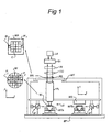
- Figure 1 schematically depicts a lithographic projection apparatus according to an embodiment of the invention.
- the apparatus comprises:
- the apparatus is of a transmissive type (i.e. has a transmissive mask). However, in general, it may also be of a reflective type, for example.
- the radiation system comprises a source LA (e.g. a Hg lamp, excimer laser, an undulator provided around the path of an electron beam in a storage ring or synchrotron, a laser plasma source or an electron or ion beam source) which produces a beam of radiation.
- a source LA e.g. a Hg lamp, excimer laser, an undulator provided around the path of an electron beam in a storage ring or synchrotron, a laser plasma source or an electron or ion beam source
- This beam is passed along various optical components comprised in the illumination system, - e.g. beam shaping optics Ex, an integrator IN and a condenser CO - so that the resultant beam PB has a desired shape and intensity distribution in its cross-section.
- the beam PB subsequently intercepts the mask MA which is held in a mask holder on a mask table MT. Having passed through the mask MA, the beam PB passes through the lens PL, which focuses the beam PB onto an exposure area C of the substrate W. With the aid of the interferometric displacement and measuring means IF, the substrate tables WTa, WTb can be moved accurately by the second and third positioning means, e.g. so as to position different exposure areas C in the path of the beam PB. Similarly, the first positioning means can be used to accurately position the mask MA with respect to the path of the beam PB, e.g. after mechanical retrieval of the mask MA from a mask library.
- the object tables MT, WTa, WTb will be realized with the aid of a long stroke module (course positioning) and a short stroke module (fine positioning), which are not explicitly depicted in Figure 1.
- the reticle table may be connected only to a short stroke positioning device, to make fine adjustments in mask orientation and position.
- the second and third positioning means may be constructed so as to be able to position their respective substrate tables WTa, WTb over a range encompassing both the exposure station under projection system PL and the measurement station under the measurement system MS.
- the second and third positioning means may be replaced by separate exposure station and measurement station positioning systems for positioning a substrate table in the respective exposure stations and a table exchange means for exchanging the substrate tables between the two positioning systems. Suitable positioning systems are described, inter alia, in WO 98/28665 and WO 98/40791 mentioned above.
- a lithography apparatus may have multiple exposure stations and/or multiple measurement stations and that the numbers of measurement and exposure stations may be different than each other and the total number of stations need not equal the number of substrate tables. Indeed, the principle of separate exposure and measurement stations may be employed even with a single substrate table.
- the depicted apparatus can be used in two different modes:
- Unflatness may be caused, for example, by variations in wafer thickness, distortion of the shape of the wafer or contaminants on the wafer holder. The presence of structures due to previous process steps also significantly affects the wafer height (flatness). Unless the context otherwise requires, references below to "the wafer surface” refer to the top surface of the wafer onto which will be projected the mask image.
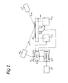
- FIG 2 a part of the measurement station region of the lithographic projection apparatus is shown.
- the substrate W is held on the substrate table WT.
- the substrate table WT is connected to actuators 12.
- These actuators 12 are connected to a control device 6 with a processor 8 and a memory 10.
- the processor 8 further receives information from position sensors 14 measuring the actual position of the wafer table WT or wafer table holder by electric (capacitive, inductive) or optical, e.g. interferometric (as shown in figure 1) means.
- the processor 8 also receives input from a level sensor LS which measures the height and/or tilt information from the target area on the wafer where the projection beam PB will hit the substrate surface.
- the control device 6 is connected to a reporting system 9, which may comprise a PC or a printer or any other registration or display device.
- the level sensor LS may be, for example, an optical sensor; alternatively, a pneumatic or capacitive sensor (for example) is conceivable.
- a presently preferred form of sensor is an optical sensor making use of Moiré patterns formed between the image of a projection grating reflected by the wafer surface and a fixed detection grating as described in US Patent 5,191,200.
- the level sensor LS should preferably measure the vertical position of one or more very small areas (e.g. 15 nm) of the wafer surface.
- the LS shown in figure 2 comprises a light source 2 for producing a light beam 16, projection optics (not shown) for projecting the light beam 16 onto the wafer W, detection optics (not shown) and a detector 15.
- the detector generates a height dependent signal, which is fed to the processor 8.
- the processor is arranged to process the height information and to construct a measured height map.
- Such a height map may be stored by the processor 8 in the memory 10.
- the term 'height map' is intended to mean a plurality of substrate height measurements, each recorded with associated X and Y co-ordinates.
- Figure 2 relates to a multi stage lithographic apparatus.
- the level sensor LS may be present in a single stage lithographic projection apparatus.
- the level sensing method uses one or more small areas and measures the average height of the small areas, referred to as sensing spots.
- a selection mechanism selects the spots, which are applicable to derive height and/or tilt information from a measured target area. For example, sensing spots outside the measured target area, will not be selected to derive height information.
- a way to solve this problem is by using extra sensing spots which cross the border of the target area. In this way all relevant areas on the wafer are sensed and are available for focus spot detection algorithms.
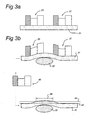
- Figure 3A shows a side view of a substrate 21 with two structures, representing two dies (target areas) 25, 27.
- the substrate 21 is flat, showing no signs of contamination underneath.
- Figure 3B shows a substrate 31 having an unflatness caused by a contamination particle 32.
- the contamination particle 32 is situated between a substrate holder, not shown, and the substrate 31. Due to the unflatness of the substrate 31, the surface of the wafer, i.e. the top surfaces of dies 35, 37 laying on top of the substrate 31, also shows an 'unflatness'.
- the processor 8 is arranged to create a measured height map out of height information received from the level sensor LS. Because of the relatively large dimensions of the structures of the dies (i.e. topology), the 'unflatness' is hidden. This means that the measured height map does contain information on the unflatness, but it will be very difficult to accurately locate and register a contamination particle.
- the lithographic projection apparatus comprises a processor 8, arranged to calculate an average die topology 40, see figure 3B, and to subtract the average die topology 40 from the measured height map for dies on the substrate, thereby producing a raw height map of the substrate surface.
- Figure 3B shows the situation after the subtraction.
- An imaginary substrate 41 is shown, without any die on top. Due to the contamination particle 32, the substrate 41 shows an unflatness.
- a smoothed height map 43 is subtracted from the raw height map. For all positions of the substrate, deviations (i.e. residuals) are calculated, resulting in a 'subtracted height map' of the substrate surface. These residuals are used to determine a standard deviation ⁇ .
- focus spots are defined as being areas on the substrate 41, in which the residual height is n times higher than ⁇ , with n being an integer or any positive real number.
- a threshold line 44 is shown which indicates a height that is n* ⁇ higher than the smoothed height map 43. Areas in which the subtracted height map exceeds the threshold line 44, are defined as focus spots 68. It is appreciated that other mathematical calculations are possible to define the threshold and the focus spots, using said 'subtracted height map'. For example, an absolute threshold Z max may be used to detect focus spots.
- the processor 8 is arranged to process the measured height map.
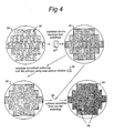
- Figure 4 shows a flow chart with four top views of the different height maps during the processing of the height map information.
- a measured height map 50 contains height information of a plurality of points on the substrate. The degree of detail of the height map is dependent on the resolution of the level sensor, which is used to measure the heights of the particular points, as will be clear to a skilled person.
- the measured height map 50 comprises height information from several dies 52.
- the processor 8 is arranged to calculate an average die topology, depicted in figure 4 by 40.
- the result is an average die topology, as shown in figure 2B, and indicated in figure 4 by reference number 40.
- the average die topology 40 is subtracted from the measured height map 50, at each of the die locations. This results in a raw height map 56 of the substrate surface.
- the raw height map 56 is smoothed using a moving average principle with a smoothing window 58.
- the processor 8 is arranged to smooth the raw height map by calculating an average height at a point x,y, i.e.
- AH(x,y) wherein the average height AH(x,y) is equal to the sum of all heights H(x i ,y i ,) in a window [ (x - a , y + a) , (x - a , y - a) , (x + a , y + a) , (x + a,y - a) ] divided by the number of points x i ,y i in said window, where a is the size of said window.
- the smoothing window 58 is preferably relatively large as compared to the expected focus spots. Typical values of the size of a focus spot is 5 * 5 mm.
- the result of the smoothing of the raw height map 56 is a smoothed height map 60, see figure 4.
- the smoothed height map 60 is subtracted from the raw height map for every x, y position of the substrate. This is indicated by the '- ' sign 64 in figure 4.
- These results in a map called the subtracted height map 66. From this subtracted height map 66 it is possible to locate local unflatnesses (i.e. hills) 68 very easily. If such unflatnesses exceed a predefined deviation threshold F, the areas in which these unflatnesses occur, are labelled as focus spots.
- different deviation thresholds are used to classify, for example, critical and less critical focus spots.
- a multi-stage apparatus for example, it is possible to reject a wafer when the wafer comprises (too many) critical focus spots, before the wafer is even processed at the exposure station. This increases yield of the apparatus.
- the processor 8 is arranged to filter out obvious errors such as measurements errors, local dirt on the substrate or a focus spots itself. This is achieved by repeating all actions shown in figure 4 but with a so-called feedback height map (not shown) instead of with a measured height map 50.
- This feedback height map is fabricated by removing height information from the subtracted height map 66 of dies that overlap with the determined focus spots 68.
- the feedback height map is used to calculate a corrected average die topology.
- the corrected average die topology is calculated in the same way as the average die topology 40, shown in figure 4, is calculated.
- the corrected average die topology is subtracted from the feedback height map for dies on the substrate. This leaves a so-called corrected raw height map of the surface of the substrate.
- the next action is to smooth the corrected raw height map using a moving average principle, as was done with the raw height map, mentioned above.
- the result is a corrected smoothed height map.
- the corrected smoothed height map from is subtracted, thereby producing a corrected subtracted height map.
- the a deviation threshold F is determined.
- the focus spots are determined as being areas in which a residual on the corrected subtracted height map is greater than the at least one deviation threshold F.
- the above actions may be repeated until a certain accuracy level is reached. By removing the height information of the dies that are on top of a focus spot, and repeating the actions mentioned above, the obvious errors are filtered out. By filtering out the obvious errors, a higher degree of accuracy can be reached.
- a second or third order polynomial fit is subtracted from the measured height map, in order to remove a global shape of said substrate.
- the global shape of the substrate may blind local focus spot information in the height maps, so subtracting a second or third order polynomial will increase the accuracy.
- fourth, fifth or even higher order polynomials may be used.
- the polynomial fit may also be subtracted from the measured height map after the average die topology has been subtracted.
- the subtracted height maps of successively provided substrates are compared, to detect correlations in the locations of any unflatnesses that may be indicative of contamination or systematic faults of said second object table.
- so-called 'chuck spots' are located, and it may be decided to clean the substrate holder.
- the location of focus spots on successive substrates is compared.
- the size of the focus spots may be taken into account. Two focus spots will then be regarded as being on the same position if they overlap, or nearly overlap. When the number of focus spots on the same position on successive wafers exceeds a certain threshold level, it will then be considered a chuck spot.
Landscapes
- Physics & Mathematics (AREA)
- General Physics & Mathematics (AREA)
- Exposure Of Semiconductors, Excluding Electron Or Ion Beam Exposure (AREA)
- Exposure And Positioning Against Photoresist Photosensitive Materials (AREA)
Priority Applications (1)
| Application Number | Priority Date | Filing Date | Title |
|---|---|---|---|
| EP04075692A EP1457828A3 (fr) | 2003-03-10 | 2004-03-03 | Supervision de points de focalisation dans un appareil de projection lithographique |
Applications Claiming Priority (3)
| Application Number | Priority Date | Filing Date | Title |
|---|---|---|---|
| EP03075698 | 2003-03-10 | ||
| EP03075698 | 2003-03-10 | ||
| EP04075692A EP1457828A3 (fr) | 2003-03-10 | 2004-03-03 | Supervision de points de focalisation dans un appareil de projection lithographique |
Publications (2)
| Publication Number | Publication Date |
|---|---|
| EP1457828A2 true EP1457828A2 (fr) | 2004-09-15 |
| EP1457828A3 EP1457828A3 (fr) | 2009-04-22 |
Family
ID=32773650
Family Applications (1)
| Application Number | Title | Priority Date | Filing Date |
|---|---|---|---|
| EP04075692A Withdrawn EP1457828A3 (fr) | 2003-03-10 | 2004-03-03 | Supervision de points de focalisation dans un appareil de projection lithographique |
Country Status (1)
| Country | Link |
|---|---|
| EP (1) | EP1457828A3 (fr) |
Cited By (10)
| Publication number | Priority date | Publication date | Assignee | Title |
|---|---|---|---|---|
| EP2128701A1 (fr) * | 2008-05-30 | 2009-12-02 | ASML Netherlands BV | Méthode de détermination de défauts dans un substrat et appareil pour exposer un substrat dans un procédé de lithographie |
| US7639345B2 (en) | 2005-10-18 | 2009-12-29 | Asml Netherlands B.V. | Lithographic apparatus |
| US7927185B2 (en) | 2006-01-30 | 2011-04-19 | Memc Electronic Materials, Inc. | Method for assessing workpiece nanotopology using a double side wafer grinder |
| US7930058B2 (en) | 2006-01-30 | 2011-04-19 | Memc Electronic Materials, Inc. | Nanotopography control and optimization using feedback from warp data |
| US8289516B2 (en) | 2007-11-20 | 2012-10-16 | Asml Netherlands B.V. | Method of measuring focus of a lithographic projection apparatus |
| CN103744271A (zh) * | 2014-01-28 | 2014-04-23 | 苏州苏大维格光电科技股份有限公司 | 一种激光直写系统与光刻方法 |
| WO2017005419A1 (fr) | 2015-07-03 | 2017-01-12 | Asml Netherlands B.V. | Appareil lithographique, procédé de commande et produit de programme informatique |
| EP3364247A1 (fr) * | 2017-02-17 | 2018-08-22 | ASML Netherlands B.V. | Procédés et appareil de surveillance d'un processus de fabrication lithographique |
| WO2019048137A1 (fr) * | 2017-09-06 | 2019-03-14 | Asml Netherlands B.V. | Procédé de détermination d'un paramètre de commande pour un appareil utilisé dans un processus de fabrication de semi-conducteurs |
| CN113160049A (zh) * | 2021-03-05 | 2021-07-23 | 深圳市普汇智联科技有限公司 | 一种基于拼接融合系统的多投影仪无缝拼接融合方法 |
Family Cites Families (1)
| Publication number | Priority date | Publication date | Assignee | Title |
|---|---|---|---|---|
| US5748323A (en) * | 1997-01-23 | 1998-05-05 | Advanced Micro Devices | Method and apparatus for wafer-focusing |
-
2004
- 2004-03-03 EP EP04075692A patent/EP1457828A3/fr not_active Withdrawn
Cited By (19)
| Publication number | Priority date | Publication date | Assignee | Title |
|---|---|---|---|---|
| US7639345B2 (en) | 2005-10-18 | 2009-12-29 | Asml Netherlands B.V. | Lithographic apparatus |
| US7927185B2 (en) | 2006-01-30 | 2011-04-19 | Memc Electronic Materials, Inc. | Method for assessing workpiece nanotopology using a double side wafer grinder |
| US7930058B2 (en) | 2006-01-30 | 2011-04-19 | Memc Electronic Materials, Inc. | Nanotopography control and optimization using feedback from warp data |
| US8145342B2 (en) | 2006-01-30 | 2012-03-27 | Memc Electronic Materials, Inc. | Methods and systems for adjusting operation of a wafer grinder using feedback from warp data |
| US8289516B2 (en) | 2007-11-20 | 2012-10-16 | Asml Netherlands B.V. | Method of measuring focus of a lithographic projection apparatus |
| US8436998B2 (en) | 2007-11-20 | 2013-05-07 | Asml Netherlands B.V. | Method of measuring focus of a lithographic projection apparatus |
| EP2128701A1 (fr) * | 2008-05-30 | 2009-12-02 | ASML Netherlands BV | Méthode de détermination de défauts dans un substrat et appareil pour exposer un substrat dans un procédé de lithographie |
| US8345231B2 (en) | 2008-05-30 | 2013-01-01 | Asml Netherlands B.V. | Method of determining defects in a substrate and apparatus for exposing a substrate in a lithographic process |
| CN103744271A (zh) * | 2014-01-28 | 2014-04-23 | 苏州苏大维格光电科技股份有限公司 | 一种激光直写系统与光刻方法 |
| WO2017005419A1 (fr) | 2015-07-03 | 2017-01-12 | Asml Netherlands B.V. | Appareil lithographique, procédé de commande et produit de programme informatique |
| US10289009B2 (en) | 2015-07-03 | 2019-05-14 | Asml Netherlands B.V. | Lithographic apparatus, control method and computer program product |
| EP3364247A1 (fr) * | 2017-02-17 | 2018-08-22 | ASML Netherlands B.V. | Procédés et appareil de surveillance d'un processus de fabrication lithographique |
| WO2018149553A1 (fr) * | 2017-02-17 | 2018-08-23 | Asml Netherlands B.V. | Procédés et appareil de surveillance d'un processus de fabrication lithographique |
| US10866527B2 (en) | 2017-02-17 | 2020-12-15 | Asml Netherlands B.V. | Methods and apparatus for monitoring a lithographic manufacturing process |
| US11422476B2 (en) | 2017-02-17 | 2022-08-23 | Asml Netherlands B.V. | Methods and apparatus for monitoring a lithographic manufacturing process |
| WO2019048137A1 (fr) * | 2017-09-06 | 2019-03-14 | Asml Netherlands B.V. | Procédé de détermination d'un paramètre de commande pour un appareil utilisé dans un processus de fabrication de semi-conducteurs |
| US11181829B2 (en) | 2017-09-06 | 2021-11-23 | Asml Netherlands B.V. | Method for determining a control parameter for an apparatus utilized in a semiconductor manufacturing process |
| CN113160049A (zh) * | 2021-03-05 | 2021-07-23 | 深圳市普汇智联科技有限公司 | 一种基于拼接融合系统的多投影仪无缝拼接融合方法 |
| CN113160049B (zh) * | 2021-03-05 | 2022-12-30 | 深圳市普汇智联科技有限公司 | 一种基于拼接融合系统的多投影仪无缝拼接融合方法 |
Also Published As
| Publication number | Publication date |
|---|---|
| EP1457828A3 (fr) | 2009-04-22 |
Similar Documents
| Publication | Publication Date | Title |
|---|---|---|
| US7012672B2 (en) | Lithographic apparatus, system, method, computer program, and apparatus for height map analysis | |
| KR100554258B1 (ko) | 리소그래피 투영장치 교정방법 및 상기 방법을 적용할 수있는 장치 | |
| KR101664962B1 (ko) | 오버레이를 보정하기 위한 정렬 마크들의 유용도를 결정하는 방법, 및 리소그래피 장치 및 오버레이 측정 시스템의 조합 | |
| US7113257B2 (en) | Assembly comprising a sensor for determining at least one of tilt and height of a substrate, a method therefor and a lithographic projection apparatus | |
| EP1231513A1 (fr) | Appareil de projection lithographique avec surface réglable de focalisation | |
| CN100495212C (zh) | 确定工艺步骤的特征的方法和器件制造方法 | |
| JP4669857B2 (ja) | 較正方法 | |
| EP2128701A1 (fr) | Méthode de détermination de défauts dans un substrat et appareil pour exposer un substrat dans un procédé de lithographie | |
| CN109313405B (zh) | 用于确定衬底上目标结构的位置的方法和设备、用于确定衬底的位置的方法和设备 | |
| US20070258074A1 (en) | Reduction of fit error due to non-uniform sample distribution | |
| TW201901289A (zh) | 判定護膜劣化補償校正之方法及相關聯微影裝置及電腦程式 | |
| US6987555B2 (en) | Lithographic apparatus, device manufacturing method, and device manufactured thereby | |
| US20190171120A1 (en) | Alignment mark recovery method and lithographic apparatus | |
| EP1139176B1 (fr) | Appareil lithographique et support de masque | |
| CN113632011A (zh) | 确定衬底上的计量点的集合的方法、关联的装置和计算机程序 | |
| JP2006179915A (ja) | リソグラフィ装置の焦点試験方法およびシステム、およびデバイス製造方法 | |
| EP1186959B1 (fr) | Méthode de calibration d'un appareil de projection lithographique | |
| US20200152527A1 (en) | Clearing out method, revealing device, lithographic apparatus, and device manufacturing method | |
| US7436485B2 (en) | Lithographic apparatus, patterning assembly and contamination estimation method | |
| CN108292111B (zh) | 用于在光刻设备中处理衬底的方法和设备 | |
| EP1357435A1 (fr) | Appareil lithographique et méthode de fabrication d'un dispositif | |
| TW202520007A (zh) | 判定微影設備上之退化的方法 | |
| EP1457839A2 (fr) | Appareil de projection lithographique avec dispositif de mesure de hauteur et d'inclinaison | |
| WO2023012338A1 (fr) | Cible de métrologie, dispositif de formation de motifs et procédé de métrologie | |
| CN120858315A (zh) | 多层量测系统和方法 |
Legal Events
| Date | Code | Title | Description |
|---|---|---|---|
| PUAI | Public reference made under article 153(3) epc to a published international application that has entered the european phase |
Free format text: ORIGINAL CODE: 0009012 |
|
| AK | Designated contracting states |
Kind code of ref document: A2 Designated state(s): AT BE BG CH CY CZ DE DK EE ES FI FR GB GR HU IE IT LI LU MC NL PL PT RO SE SI SK TR |
|
| AX | Request for extension of the european patent |
Extension state: AL LT LV MK |
|
| RAP1 | Party data changed (applicant data changed or rights of an application transferred) |
Owner name: ASML NETHERLANDS B.V. |
|
| PUAL | Search report despatched |
Free format text: ORIGINAL CODE: 0009013 |
|
| AK | Designated contracting states |
Kind code of ref document: A3 Designated state(s): AT BE BG CH CY CZ DE DK EE ES FI FR GB GR HU IE IT LI LU MC NL PL PT RO SE SI SK TR |
|
| AX | Request for extension of the european patent |
Extension state: AL LT LV MK |
|
| AKX | Designation fees paid |
Designated state(s): DE FR GB IT NL |
|
| STAA | Information on the status of an ep patent application or granted ep patent |
Free format text: STATUS: THE APPLICATION IS DEEMED TO BE WITHDRAWN |
|
| 18D | Application deemed to be withdrawn |
Effective date: 20091001 |