EP1458030A2 - Nouveaux éléments conducteurs pour des transistors à couche mince utilisés dans un écran plat - Google Patents
Nouveaux éléments conducteurs pour des transistors à couche mince utilisés dans un écran plat Download PDFInfo
- Publication number
- EP1458030A2 EP1458030A2 EP04250862A EP04250862A EP1458030A2 EP 1458030 A2 EP1458030 A2 EP 1458030A2 EP 04250862 A EP04250862 A EP 04250862A EP 04250862 A EP04250862 A EP 04250862A EP 1458030 A2 EP1458030 A2 EP 1458030A2
- Authority
- EP
- European Patent Office
- Prior art keywords
- layer
- electrode
- thin film
- tft
- aluminum alloy
- Prior art date
- Legal status (The legal status is an assumption and is not a legal conclusion. Google has not performed a legal analysis and makes no representation as to the accuracy of the status listed.)
- Withdrawn
Links
Images




Classifications
-
- G—PHYSICS
- G02—OPTICS
- G02F—OPTICAL DEVICES OR ARRANGEMENTS FOR THE CONTROL OF LIGHT BY MODIFICATION OF THE OPTICAL PROPERTIES OF THE MEDIA OF THE ELEMENTS INVOLVED THEREIN; NON-LINEAR OPTICS; FREQUENCY-CHANGING OF LIGHT; OPTICAL LOGIC ELEMENTS; OPTICAL ANALOGUE/DIGITAL CONVERTERS
- G02F1/00—Devices or arrangements for the control of the intensity, colour, phase, polarisation or direction of light arriving from an independent light source, e.g. switching, gating or modulating; Non-linear optics
- G02F1/01—Devices or arrangements for the control of the intensity, colour, phase, polarisation or direction of light arriving from an independent light source, e.g. switching, gating or modulating; Non-linear optics for the control of the intensity, phase, polarisation or colour
- G02F1/13—Devices or arrangements for the control of the intensity, colour, phase, polarisation or direction of light arriving from an independent light source, e.g. switching, gating or modulating; Non-linear optics for the control of the intensity, phase, polarisation or colour based on liquid crystals, e.g. single liquid crystal display cells
- G02F1/133—Constructional arrangements; Operation of liquid crystal cells; Circuit arrangements
- G02F1/136—Liquid crystal cells structurally associated with a semi-conducting layer or substrate, e.g. cells forming part of an integrated circuit
-
- H—ELECTRICITY
- H10—SEMICONDUCTOR DEVICES; ELECTRIC SOLID-STATE DEVICES NOT OTHERWISE PROVIDED FOR
- H10D—INORGANIC ELECTRIC SEMICONDUCTOR DEVICES
- H10D30/00—Field-effect transistors [FET]
- H10D30/60—Insulated-gate field-effect transistors [IGFET]
- H10D30/67—Thin-film transistors [TFT]
- H10D30/6729—Thin-film transistors [TFT] characterised by the electrodes
- H10D30/6737—Thin-film transistors [TFT] characterised by the electrodes characterised by the electrode materials
- H10D30/6739—Conductor-insulator-semiconductor electrodes
-
- H—ELECTRICITY
- H10—SEMICONDUCTOR DEVICES; ELECTRIC SOLID-STATE DEVICES NOT OTHERWISE PROVIDED FOR
- H10D—INORGANIC ELECTRIC SEMICONDUCTOR DEVICES
- H10D30/00—Field-effect transistors [FET]
- H10D30/60—Insulated-gate field-effect transistors [IGFET]
- H10D30/67—Thin-film transistors [TFT]
- H10D30/6729—Thin-film transistors [TFT] characterised by the electrodes
-
- H—ELECTRICITY
- H10—SEMICONDUCTOR DEVICES; ELECTRIC SOLID-STATE DEVICES NOT OTHERWISE PROVIDED FOR
- H10D—INORGANIC ELECTRIC SEMICONDUCTOR DEVICES
- H10D30/00—Field-effect transistors [FET]
- H10D30/60—Insulated-gate field-effect transistors [IGFET]
- H10D30/67—Thin-film transistors [TFT]
- H10D30/6729—Thin-film transistors [TFT] characterised by the electrodes
- H10D30/673—Thin-film transistors [TFT] characterised by the electrodes characterised by the shapes, relative sizes or dispositions of the gate electrodes
-
- H—ELECTRICITY
- H10—SEMICONDUCTOR DEVICES; ELECTRIC SOLID-STATE DEVICES NOT OTHERWISE PROVIDED FOR
- H10D—INORGANIC ELECTRIC SEMICONDUCTOR DEVICES
- H10D30/00—Field-effect transistors [FET]
- H10D30/60—Insulated-gate field-effect transistors [IGFET]
- H10D30/67—Thin-film transistors [TFT]
- H10D30/6729—Thin-film transistors [TFT] characterised by the electrodes
- H10D30/6737—Thin-film transistors [TFT] characterised by the electrodes characterised by the electrode materials
-
- H—ELECTRICITY
- H10—SEMICONDUCTOR DEVICES; ELECTRIC SOLID-STATE DEVICES NOT OTHERWISE PROVIDED FOR
- H10D—INORGANIC ELECTRIC SEMICONDUCTOR DEVICES
- H10D30/00—Field-effect transistors [FET]
- H10D30/60—Insulated-gate field-effect transistors [IGFET]
- H10D30/67—Thin-film transistors [TFT]
- H10D30/674—Thin-film transistors [TFT] characterised by the active materials
- H10D30/6741—Group IV materials, e.g. germanium or silicon carbide
- H10D30/6743—Silicon
-
- H—ELECTRICITY
- H10—SEMICONDUCTOR DEVICES; ELECTRIC SOLID-STATE DEVICES NOT OTHERWISE PROVIDED FOR
- H10D—INORGANIC ELECTRIC SEMICONDUCTOR DEVICES
- H10D86/00—Integrated devices formed in or on insulating or conducting substrates, e.g. formed in silicon-on-insulator [SOI] substrates or on stainless steel or glass substrates
Definitions
- the present invention relates to a flat panel display thin film transistors. More particularly, the present invention relates to a novel structure for electrodes of the thin film transistors that do not degrade the semiconductor material of the thin film transistors in the display.
- a thin film transistor (hereinafter TFT) is a device of which a source electrode and a drain electrode can be electrically connected through a channel formed in a semiconductor layer which physically connects the source and drain electrodes according to a voltage applied to a gate electrode.
- the TFT is mainly used in an active matrix flat panel display such as an electroluminescent display and a liquid crystal display.
- the TFT serves to independently drive sub-pixels in a flat panel display.
- a source electrode and a gate electrode formed on a TFT panel of a flat panel display are connected to driving circuits arranged on sides of the flat panel display through conductive lines.
- the source electrode, the drain electrode and the conductive lines electrically connected to the source and drain electrodes are at the same time formed with the same structure using the same material for the sake of simplifying a manufacturing process.
- the source electrode, the drain electrode, and the conductive lines electrically connected thereto are simply referred to as "S/D electrodes and lead lines".
- the S/D electrodes and lead lines may be made of a chromium (Cr) based metal or a molybdenum (Mo) based metal such as Mo and MoW.
- Cr chromium
- Mo molybdenum
- these metals are relatively impractical for forming the S/D electrodes and lead lines for use in a large flat panel display.
- aluminum Al
- use of pure Al has a problem in that the aluminum diffuses toward and into a semiconductor layer during a heat treatment process that generally occurs subsequent to formation of the source electrode and the drain electrode. When the aluminum diffuses into the semiconductor layer, the TFT does not function properly.
- Tanaka '157 discloses electrodes made of Al.
- Each of the electrodes has a structure of titanium nitride (TiN)/Al, TiN/Ti/Al, or TiN/Al/Ti.
- TiN titanium nitride
- TiN/Ti/Al TiN/Ti/Al
- TiN/Al/Ti TiN/Al/Ti.
- Advantages of such a structure include reduction of an electrical connection resistance between the electrodes and terminals connected to the electrodes and suppression of generation of Al hillocks often formed during a heat treatment process subsequent to the formation of the electrodes.
- this Tanaka '157 fails to discuss the existence of and a solution to the problem of aluminum from a pure aluminum electrode from diffusing into a semiconductor layer of a transistor during a heat treatment process.
- TiAl 3 may be generated at an interface between the pure Al layer and the Ti layer by a heat treatment process.
- the TiAl 3 may increase the resistance of the conductive lines.
- a voltage drop between driving circuits and the pixels may increase when TiAl 3 is formed.
- the formation of TiAl 3 causes the response speed of the pixels to decrease and causes a non-uniform distribution of an image in a large display.
- a thin film transistor comprising a source electrode, a drain electrode, a gate electrode and a semiconductor layer, wherein one of the source electrode, the drain electrode, and the gate electrode comprises an aluminum alloy layer disposed between a pair of titanium layers.
- a flat panel display comprising: a substrate; a first plurality of thin film transistors formed on a surface of the substrate, the first plurality of thin film transistors comprising first source electrodes, first drain electrodes, first gate electrodes, and semiconductor layers; a plurality of first conductive lines electrically connected to the first source electrodes; and a plurality of second conductive lines electrically connected to the first gate electrodes; a second plurality of thin film transistors, wherein the first drain electrodes of the first plurality of thin film transistors are electrically connected to gate electrodes of the second plurality of thin film transistors, wherein one of the first source electrodes, the first drain electrodes, the first gate electrodes, the plurality of first conductive lines, and the plurality of second conductive lines comprises an aluminum alloy layer and a titanium layer formed on one surface of the aluminum alloy layer.
- a thin film transistor comprising: a source electrode, a gate electrode and a drain electrode; and a semiconductor layer between the source electrode and the drain electrode, wherein one of said source electrode and said drain electrode contain an aluminum alloy layer and not a pure aluminum layer.
- an electrode structure where aluminum is used but aluminum is not used in pure form. Instead, an alloy of aluminum is used in the electrodes.
- the aluminum alloy layer may contain about 0.1 to 5 wt% of at least one element selected from silicon, copper, neodymiumm, platinum, and nickel.
- the reason why an aluminum alloy and not pure aluminum should be used is because after being subject to a heat treatment, aluminum from a pure aluminum layer will diffuse into the semiconductor layer and corrupt the electrical properties of the TFT. By using an aluminum alloy and not pure aluminum in the electrode structure, the diffusion of aluminum into the semiconductor layer during a heat treatment is prevented.
- the aluminum alloy layer may be bounded by titanium.
- a diffusion prevention layer may be interposed between the aluminum alloy layer and the titanium layer.
- the diffusion prevention layer is TiN or titanium nitride.
- Optimum TiN thickness is 300 ⁇ .
- the TiN layer may have 5 to 85 wt% of nitrogen.
- the present invention may provide an improved design for S/D electrodes and lead lines for TFT's used in a flat panel display.
- the present invention may provide a design for electrodes in a TFT that prevent aluminum from diffusing into a semiconductor layer during a heat treatment.
- the present invention may provide a novel design for electrodes in a TFT that have a low resistivity and thus result in uniform luminance even when the display size is very large.
- the present invention may provide a design for electrodes in a TFT that does not result in a structure where the electrode material reacts with the semiconductive material of the TFT when subject to heat treatment.
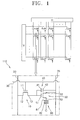
- FIG. 1 illustrates a circuit 112 for a flat panel display having a thin film transistors (TFT's) 10 and 50.
- the circuit 112 includes a first TFT 10, a second TFT 50, a storage capacitor 40, and a light emission unit 60.
- a first source electrode 12 in the first TFT 10 is connected to a horizontal driving circuit H through a first conductive line 20 and a first gate electrode 11 in the first TFT 10 is connected to a vertical driving circuit V through a second conductive line 30.
- a first drain electrode 13 in the first TFT 10 is connected to a first capacitor electrode 41 of the storage capacitor 40 and to a second gate electrode 51 of the second TFT 50.
- a second capacitor electrode 42 of the storage capacitor 40 and a second source electrode 52 of the second TFT 50 are connected to a third conductive line 70.
- a second drain electrode 53 of the second TFT 50 is connected to a first pixel electrode 61 of the light emission unit 60.
- a second pixel electrode 62 of the light emission unit 60 is arranged to be opposite to the first pixel electrode 61 and spaced a predetermined gap apart from the first pixel electrode 61.
- the active layer may be an organic material layer, an inorganic material layer, or a liquid crystal layer. This active layer is arranged between the first pixel electrode 61 and second pixel electrode 62 of the light emission unit 60 according to one of the various types of flat panel displays.
- FIG. 2 illustrates a driving unit (one of red component, blue component, and green component that constitute one pixel) of a flat panel display provided with the first TFT 10 and the second TFT 50.
- FIG. 2 is a schematic plan view illustrating a physical structure of the circuit 112 illustrated in FIG. 1.
- nonconductive constitutional elements such as a substrate, a buffer layer, various types of insulating layers, a planarization layer, a light emission layer, a liquid crystal layer, a second pixel electrode, a polarization layer, an orientation layer, and a color filter layer are omitted.
- These nonconductive constitutional elements are instead illustrated in FIGS. 3 and 4. Only constitutional elements positioned at regions represented by oblique (or slanted) lines shown in FIG. 2 are electrically connected to each other. Other regions in FIG. 2 that are not represented by oblique lines are electrically insluated.
- a conductive channel is formed in a semiconductor layer 80 that connects the first source electrode 12 to the first drain electrode 13.
- the charge moves into the first drain electrode 13.
- Another charge is supplied into the second source electrode 52 through the third conductive line 70.
- Luminance of the driving unit is determined according to the charge supplied into the second source electrode 52.
- the charge of the first drain electrode 13 is supplied to the second gate electrode 51, the charge of the second source electrode 52 moves into the second drain electrode 53, thereby driving the first pixel electrode 61 of the light emission unit 60.
- the storage capacitor 40 serves to maintain a driving operation of the first pixel electrode 61 or to increase a driving speed.
- the first TFT 10 and the second TFT 50 have a similar section structure, but are different in adjoining constitutional elements.
- An electroluminescent display 114 illustrated in FIG. 3 includes a TFT panel, a light emission layer 87, and a second pixel electrode 62.
- the TFT panel includes a substrate 81, a TFT 50, a first conductive line 20, a second conductive line 30, and a first pixel electrode 61.
- the substrate 81 may be made of a transparent material, for example glass, and the second pixel electrode 62 may be made of a metal material with good reflectivity.
- the second pixel electrode 62 may be made of a transparent conductive material, for example, indium tin oxide (ITO), and the first pixel electrode 61 may be made of a metal material with good reflectivity.
- ITO indium tin oxide
- a buffer layer 82 is formed on the whole surface of the substrate 81.
- a semiconductor layer 80 is formed to a predetermined pattern on the buffer layer 82.
- a first insulating layer 83 is formed on the semiconductor layer 80 and on the remaining exposed surface of the buffer layer 82 where the semiconductor layer 80 is not formed.
- a second gate electrode 51 is formed to a predetermined pattern on the first insulating layer 83.
- a second insulating layer 84 is formed on the second gate electrode 51 and the remaining exposed surface of the first insulating layer 83 on where the second gate electrode 51 is not formed.
- the first and second insulating layers 83 and 84 respectively are subjected to etching such as dry etching to expose portions of the semiconductor layer 80.
- the exposed portions of the semiconductor layer 80 are connected to a second source electrode 52 and a second drain electrode 53 that are formed to a predetermined pattern.
- a third insulating layer 85 is formed thereon. A portion of the third insulating layer 85 is etched to electrically connect the second drain electrode 53 and the first pixel electrode 61.
- a planarization layer 86 is formed. The portion of the planarization layer 86 corresponding to the first pixel electrode 61 is etched. Then, the light emission layer 87 is formed on the first pixel electrode 61 and the second pixel electrode 62 is formed on the light emission layer 87.
- encapsulation layer 89 is formed over second pixel electrode 62.
- the TFT 50 made up of the second source electrode 52, the second drain electrode 53, the second gate electrode 51 and the semiconductor layer 80.
- the second source electrode 52 and the second drain electrode 53 are arranged on the same horizontal plane and are separated from each other by a predetermined gap.
- the second source electrode 52 and the second drain electrode 53 are each physically connected to the semiconductor layer 80.
- the second gate electrode 51 is electrically insulated from the second source electrode 52, the second drain electrode 53 and the semiconductor layer 80.
- the second gate electrode 51 is positioned above the semiconductor layer 80 and between the second source electrode 52 and the second drain electrode 53.
- a TFT is divided into a staggered type, an inverted staggered type, a coplanar type, and an inverted coplanar type according to the arrangements of the above electrodes and the semiconductor layer 80.
- a coplanar type is illustrated in this embodiment of the present invention, but the present invention is not limited thereto.
- the TFT 50 of FIG. 3 corresponds to the second TFT 50 illustrated in FIG. 2.
- the second source electrode 52 is connected to the third conductive line 70
- the second gate electrode 51 is connected to the first drain electrode 13 of the first TFT 10
- the second drain electrode 53 is connected to the first pixel electrode 61 of light emitting unit 60
- the first source electrode 12 of the first TFT 10 is connected to the first conductive line 20
- the first gate electrode 11 is connected to the second conductive line 30.
- the first conductive line 20 corresponds to a data line for transmitting data
- the second conductive line 30 corresponds to a scan line.
- an electroluminescent display 114 includes the first pixel electrode 61, the light emission layer 87 formed on the first pixel electrode 61, and the second pixel electrode 62 formed on the light emission layer 87.
- the electroluminescent display 114 can be divided into organic and inorganic electroluminescent displays.
- the light emission layer 87 is made up of an electron transport layer, a light emission material layer, and a hole transport layer.
- insulating layers are interposed between the first pixel electrode 61 and the light emission layer 87 and between the second pixel electrode 62 and the light emission layer 87.
- the light emission material layer 87 of an organic electroluminescent display is made of an organic material, for example, phthalocyanine such as copper phthalocyanine (CuPc), N,N'-di(naphthalene- 1-yl)-N,N'-diphenyl benzidine (NPB), tris-8-hydroxyquinoline aluminium (Alq3) or the like.
- phthalocyanine such as copper phthalocyanine (CuPc), N,N'-di(naphthalene- 1-yl)-N,N'-diphenyl benzidine (NPB), tris-8-hydroxyquinoline aluminium (Alq3) or the like.
- an inorganic material layer between the insulating layers positioned at inner sides of the first pixel electrode 61 and second pixel electrode 62 emits light.
- An inorganic material for the inorganic material layer may be metal sulfide such as ZnS, SrS, and CsS. Recently, alkaline earth-based calcium sulfide such as CaCa 2 S 4 and SrCa 2 S 4 , and metal oxide are also used. Transition metal such as Mn, Ce, Tb, Eu, Tm, Er, Pr, and Pb and alkaline rare earth metal may be used as light emitting core atoms that form the light emission layer 87 together with the above inorganic material.
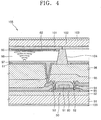
- FIG. 4 illustrates a liquid crystal display 105.
- a liquid crystal display and an electroluminescent display are similar to each other in terms of the structure of a TFT panel, but are different in adjoining constitutional elements.
- adjoining constitutional elements of the TFT panel in a liquid crystal display will be described.
- the liquid crystal display 105 includes a TFT panel, a first orientation layer 97, a second substrate 102, a second pixel electrode 62, a second orientation layer 99, a liquid crystal layer 98, and a polarization layer 103.
- the TFT panel comprises a first substrate 91, a TFT 50, a first conductive line, a second conductive line, and a first pixel electrode 61.
- the first substrate 91 corresponds to the substrate of an electroluminescent display.
- the first substrate 91 and the second substrate 102 are separately manufactured.
- a color filter layer 101 is formed on the lower surface of the second substrate 102.
- the second pixel electrode 62 is formed on the lower surface of the color filter layer 101.
- the first orientation layer 97 and the second orientation layer 99 are formed on the upper surface of the first pixel electrode 61 and the lower surface of the second pixel electrode 62, respectively.
- the first and second orientation layers 97 and 99 serve to allow for a proper orientation of a liquid crystal of the liquid crystal layer 98 interposed therebetween.
- the polarization layer 103 is formed on each of the outer surfaces of the first and second substrates 91 and 102 respectively.
- a spacer 104 is used to maintain a gap between the first substrate 91 and the second substrates 102.
- Reference numerals 92, 93, 94, 95 and 96 in FIG. 4 represent a buffer layer, a first insulating layer, a second insulating layer, a third insulating layer and a planarization
- a liquid crystal display allows light to pass through or be blocked according to the arrangement of a liquid crystal.
- the arrangement of the liquid crystal is determined by an electric potential difference between the first and second pixel electrodes.
- Light that has passed through the liquid crystal layer exhibits a color of the color filter layer 101, thereby displaying an image.
- FIG. 5 illustrates a cross section of a TFT after heat treatment using electrodes having pure aluminum and FIG. 6 is a top view of the TFT after heat treatment.
- FIG. 5 illustrates a semiconductor layer 80 arranged below and connected to S/D electrodes and lead lines 52 and 53, each of which has a three-layer structure of titanium (Ti) layer (thickness: 500 ⁇ ) 232 /pure Al layer (thickness: 4,000 ⁇ ) 231 /Ti layer (thickness: 500 ⁇ ) 233, after heat treatment at 450°C.
- Ti titanium
- the Al of the pure Al layer 231 diffuses towards and into the semiconductor layer 80 when heat is applied to thereby form diffusion defect portions 52a and 53a in the semiconductor layer 80.
- the reason the Al of the pure Al layer 231 can diffuse towards and into the semiconductor layer 80 even though a Ti layer 233 is interposed between the pure Al layer 231 and the semiconductor layer 80 is that the Ti layer 233 is present in the form of a very thin film and/or there exists a Ti-free zone in Ti layer 233 according to the upper surface structure of the semiconductor layer 80.
- the presence of a thin titanium layer 233 between the pure aluminum layer 231 of the electrode and the semiconductor layer 80 of a TFT does not prevent aluminum from the pure aluminum layer 231 from diffusing into and destroying parts of semiconductor layer 80 when heat is applied.
- the presence of a TiN diffusion layer between a titanium layer and a pure aluminum layer will not prevent aluminum from diffusing into the semiconductor layer 80 when heat is applied.
- the resultant diffusion defect portions 52a and 53a may cause the same results as when pure aluminum is deposited directly onto the semiconductor layer 80. Defect portions 52a and 53a can prevent formation of a normal conductive channel between the source electrode and the drain electrode of a TFT. Furthermore, defect portions 52a and 53a may result in a short between the source electrode and the drain electrode, resulting in a malfunctioning TFT.
- FIGS. 5 and 6 illustrate the source 52 and the drain 53 electrodes of second TFT 50, the same applies to first TFT 10.
- the first and second gate electrodes 11 and 53 are formed simultaneously with the second conductive line 30 using the same material.
- the first and second source electrodes 12 and 52, the first and second drain electrodes 13 and 53, the first conductive line 30, and the third conductive line 70 are at the same time formed using the same material. Since the formation sequences and materials for these conductive constitutional elements may vary according to manufacture processes, they are not limited to those described in this embodiment of the present invention.
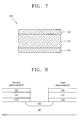
- At least one of S/D electrodes and lead lines 130 is made out of an aluminum (Al) alloy layer 131, and titanium (Ti) layers 132 and 133 formed on the respective upper and lower surfaces of the Al alloy layer 131.
- diffusion prevention layers 138 and 139 made of titanium nitride (TiN), for example, may be interposed between the Al alloy layer 131 and the respective Ti layers 132 and/or 133. Aluminum diffusion can be prevented during a heat treatment when an aluminum alloy as opposed to pure aluminum is used in the electrode structure.
- the Al alloy layer 131 is made of an alloy that contains 0.1 to 5 wt%, preferably 2 wt% of at least one element selected from silicon (Si), copper (Cu), neodymium (Nd), platinum (Pt), and nickel (Ni). It has been determined empirically that when the S/D electrodes and lead lines according to this embodiment of the present invention as illustrated in FIG.
- the S/D electrodes and lead lines have a three layer structure of Ti layer (thickness: 500 ⁇ ) 132 /Al alloy layer (thickness: 4,000 ⁇ ) 131 /Ti layer (thickness: 500 ⁇ ) 133 as illustrated in FIG. 8, the same result was obtained.
- the structure of FIG. 8 like the structure of FIG. 10, produced a semiconductor layer 80 as in FIG. 9 free from defect regions 52a and 53a.
- titanium layers 132 and 133 are used instead of just an aluminum alloy layer 131 as the titanium layers 132 and 133 serve to prevent the formation of aluminum hillocks during heat treatment.
- a five layer electrode stack of FIG. 10 is employed where TiN diffusion prevention layers 138 (139) are interposed between each titanium layer 132 (133) and the aluminum alloy layer 131 to prevent the formation of unwanted TiAl 3 during a heat treatment process.
- TiAl 3 greatly increases the resistivity of the electrodes and the conductive lines. Therefore, TiN diffusion prevention layers 138 and 139 prevent TiAl 3 from forming thus keeping the resistivity of the electrodes and the conductive lines leading to the TFT low. This is particularly important in large flat panel displays where a low resistivity of electrodes and lead lines can prevent a non-uniform pixel display distribution.
- FIGS. 8, 9 and 10 have been discussed in conjunction with second TFT 50 having a source electrode 52 and a drain electrode 53, the novel structures of FIGS. 8, 9 and 10 equally apply to the first TFT 10 as well.
- An optimum thickness of the TiN diffusion prevention layers 138 and 139 is 250 ⁇ . If the thickness of the diffusion prevention layers are too thin, Al diffusion may occur, resulting in the formation of TiAl 3 during a heat treatment. On the other hand; if the TiN diffusion layers are too thick, the production cost becomes unnecessarily too high because of the unnecessarily thick TiN layers.
- the TiN layers 138 and 139 contain 5 to 85 wt% of nitrogen.
- the Al alloy layer 131 and the Ti layers 132 and 133 are deposited by DC-magnetron sputtering under an argon (Ar) gas atmosphere.
- the TiN layers 138 and 139 are deposited by reactive sputtering under a mixed gas atmosphere of Ar and nitrogen (N 2 ).
- Such a deposited structure is etched to a predetermined pattern for the S/D electrodes and lead lines by dry etching with high frequency-enhanced plasma.
- FIGS. 5 through 10 discuss second TFT 50 and second source electrode 52 and second drain electrode 53, FIGS. 5 through 10 and the concepts discussed in the discussion of FIGS. 5 through 10 above equally apply to the first TFT 10 having first source electrode 12 and first drain electrode 13.
- the present invention provides a novel structure for an electrode attached to a semiconductor layer in a TFT that does not form defect regions in the semiconductor layer when exposed to a heat treatment. Furthermore, the resistivity is kept low.
- Other embodiments include the presence of titanium layers to prevent the formation of aluminum hillocks during heat treatment process.
- Further embodiments include the presence of a TiN diffusion layer between the aluminum alloy layer and the titanium layers to prevent the formation of highly resistive TiAl 3 during heat treatment.
Landscapes
- Physics & Mathematics (AREA)
- Nonlinear Science (AREA)
- Mathematical Physics (AREA)
- Engineering & Computer Science (AREA)
- Chemical & Material Sciences (AREA)
- Crystallography & Structural Chemistry (AREA)
- Microelectronics & Electronic Packaging (AREA)
- General Physics & Mathematics (AREA)
- Optics & Photonics (AREA)
- Thin Film Transistor (AREA)
- Liquid Crystal (AREA)
- Electrodes Of Semiconductors (AREA)
- Electroluminescent Light Sources (AREA)
- Devices For Indicating Variable Information By Combining Individual Elements (AREA)
Applications Claiming Priority (2)
| Application Number | Priority Date | Filing Date | Title |
|---|---|---|---|
| KR2003015357 | 2003-03-12 | ||
| KR1020030015357A KR100669688B1 (ko) | 2003-03-12 | 2003-03-12 | 박막트랜지스터 및 이를 구비한 평판표시소자 |
Publications (2)
| Publication Number | Publication Date |
|---|---|
| EP1458030A2 true EP1458030A2 (fr) | 2004-09-15 |
| EP1458030A3 EP1458030A3 (fr) | 2006-03-15 |
Family
ID=32768636
Family Applications (1)
| Application Number | Title | Priority Date | Filing Date |
|---|---|---|---|
| EP04250862A Withdrawn EP1458030A3 (fr) | 2003-03-12 | 2004-02-18 | Nouveaux éléments conducteurs pour des transistors à couche mince utilisés dans un écran plat |
Country Status (5)
| Country | Link |
|---|---|
| US (2) | US20040183072A1 (fr) |
| EP (1) | EP1458030A3 (fr) |
| JP (1) | JP2004282066A (fr) |
| KR (1) | KR100669688B1 (fr) |
| CN (1) | CN100351691C (fr) |
Cited By (4)
| Publication number | Priority date | Publication date | Assignee | Title |
|---|---|---|---|---|
| EP1458029A2 (fr) * | 2003-03-12 | 2004-09-15 | Samsung SDI Co., Ltd. | Noveaux éléments conducteurs pour des transistors à couche mince utilisés dans un écran plat |
| US7492028B2 (en) | 2005-02-18 | 2009-02-17 | Semiconductor Energy Laboratory Co., Ltd. | Photoelectric conversion device and manufacturing method of the same, and a semiconductor device |
| WO2011120060A3 (fr) * | 2010-03-29 | 2011-12-01 | Ctr Carinthian Tech Research Ag | Couches minces électroconductrices résistant aux températures élevées |
| EP3723131A3 (fr) * | 2019-01-25 | 2020-11-11 | Samsung Display Co., Ltd. | Ligne conductrice pour dispositif d'affichage, dispositif d'affichage la comprenant et procédé de fabrication d'un dispositif d'affichage la comprenant |
Families Citing this family (20)
| Publication number | Priority date | Publication date | Assignee | Title |
|---|---|---|---|---|
| KR100799824B1 (ko) * | 2005-08-17 | 2008-01-31 | 가부시키가이샤 고베 세이코쇼 | 소스/드레인 전극, 트랜지스터 기판 및 그의 제조 방법, 및표시 디바이스 |
| US7683370B2 (en) | 2005-08-17 | 2010-03-23 | Kobe Steel, Ltd. | Source/drain electrodes, transistor substrates and manufacture methods, thereof, and display devices |
| KR101251351B1 (ko) * | 2005-12-28 | 2013-04-05 | 삼성디스플레이 주식회사 | 박막트랜지스터 기판, 이의 제조방법 및 이를 갖는표시패널 |
| KR100774950B1 (ko) * | 2006-01-19 | 2007-11-09 | 엘지전자 주식회사 | 전계발광소자 |
| RU2401520C2 (ru) * | 2006-04-27 | 2010-10-10 | Улвак, Инк. | Устройство отображения и составное устройство отображения |
| JP5214858B2 (ja) | 2006-06-22 | 2013-06-19 | 三菱電機株式会社 | Tftアレイ基板及びその製造方法 |
| JP5016712B2 (ja) * | 2010-09-21 | 2012-09-05 | 三井金属鉱業株式会社 | 電極箔および有機デバイス |
| US8841733B2 (en) | 2011-05-17 | 2014-09-23 | United Microelectronics Corp. | Semiconductor device and method of fabricating the same |
| JP2013084907A (ja) * | 2011-09-28 | 2013-05-09 | Kobe Steel Ltd | 表示装置用配線構造 |
| US20150295092A1 (en) * | 2012-10-01 | 2015-10-15 | Sharp Kabushiki Kaisha | Semiconductor device |
| US9899598B2 (en) * | 2013-05-01 | 2018-02-20 | Konica Minolta, Inc. | Organic electroluminescent element |
| JP2017503564A (ja) * | 2013-12-18 | 2017-02-02 | ノヴォクセル リミテッド | 組織気化装置および方法 |
| TWI535034B (zh) * | 2014-01-29 | 2016-05-21 | 友達光電股份有限公司 | 畫素結構及其製作方法 |
| US9548349B2 (en) * | 2014-06-25 | 2017-01-17 | International Business Machines Corporation | Semiconductor device with metal extrusion formation |
| CN104241392B (zh) * | 2014-07-14 | 2017-07-14 | 京东方科技集团股份有限公司 | 一种薄膜晶体管及其制备方法、显示基板和显示设备 |
| CN106531768A (zh) * | 2016-12-07 | 2017-03-22 | 厦门天马微电子有限公司 | 一种有机电致发光显示面板及其制备方法 |
| KR20190043194A (ko) * | 2017-10-17 | 2019-04-26 | 삼성디스플레이 주식회사 | 금속 배선 및 이를 포함하는 박막 트랜지스터 |
| KR102839408B1 (ko) | 2019-01-17 | 2025-07-28 | 삼성디스플레이 주식회사 | 표시 장치 및 이의 제조 방법 |
| KR102819170B1 (ko) * | 2019-02-18 | 2025-06-12 | 삼성디스플레이 주식회사 | 표시 장치 및 이의 제조 방법 |
| KR102942090B1 (ko) * | 2020-07-16 | 2026-03-20 | 삼성디스플레이 주식회사 | 표시 장치 |
Citations (1)
| Publication number | Priority date | Publication date | Assignee | Title |
|---|---|---|---|---|
| JP2003015105A (ja) * | 2001-06-28 | 2003-01-15 | Hitachi Ltd | 画像表示装置 |
Family Cites Families (61)
| Publication number | Priority date | Publication date | Assignee | Title |
|---|---|---|---|---|
| US4153529A (en) * | 1975-04-21 | 1979-05-08 | Hughes Aircraft Company | Means and method for inducing uniform parallel alignment of liquid crystal material in a liquid crystal cell |
| DE3242831A1 (de) * | 1982-11-19 | 1984-05-24 | Siemens AG, 1000 Berlin und 8000 München | Solarzelle aus amorphem silizium und verfahren zu ihrer herstellung |
| US5278099A (en) * | 1985-05-13 | 1994-01-11 | Kabushiki Kaisha Toshiba | Method for manufacturing a semiconductor device having wiring electrodes |
| US4933296A (en) * | 1985-08-02 | 1990-06-12 | General Electric Company | N+ amorphous silicon thin film transistors for matrix addressed liquid crystal displays |
| US4646424A (en) * | 1985-08-02 | 1987-03-03 | General Electric Company | Deposition and hardening of titanium gate electrode material for use in inverted thin film field effect transistors |
| US4782380A (en) * | 1987-01-22 | 1988-11-01 | Advanced Micro Devices, Inc. | Multilayer interconnection for integrated circuit structure having two or more conductive metal layers |
| US4910580A (en) * | 1987-08-27 | 1990-03-20 | Siemens Aktiengesellschaft | Method for manufacturing a low-impedance, planar metallization composed of aluminum or of an aluminum alloy |
| US4778258A (en) * | 1987-10-05 | 1988-10-18 | General Electric Company | Protective tab structure for use in the fabrication of matrix addressed thin film transistor liquid crystal displays |
| JPH0666287B2 (ja) * | 1988-07-25 | 1994-08-24 | 富士通株式会社 | 半導体装置の製造方法 |
| US5244820A (en) * | 1990-03-09 | 1993-09-14 | Tadashi Kamata | Semiconductor integrated circuit device, method for producing the same, and ion implanter for use in the method |
| US5243202A (en) * | 1990-04-25 | 1993-09-07 | Casio Computer Co., Ltd. | Thin-film transistor and a liquid crystal matrix display device using thin-film transistors of this type |
| US5345108A (en) * | 1991-02-26 | 1994-09-06 | Nec Corporation | Semiconductor device having multi-layer electrode wiring |
| JP2533414B2 (ja) * | 1991-04-09 | 1996-09-11 | 三菱電機株式会社 | 半導体集積回路装置の配線接続構造およびその製造方法 |
| US5485019A (en) * | 1992-02-05 | 1996-01-16 | Semiconductor Energy Laboratory Co., Ltd. | Semiconductor device and method for forming the same |
| JP3587537B2 (ja) * | 1992-12-09 | 2004-11-10 | 株式会社半導体エネルギー研究所 | 半導体装置 |
| JPH06188265A (ja) * | 1992-12-22 | 1994-07-08 | Matsushita Electric Ind Co Ltd | 半導体装置およびその製造方法 |
| JPH06250211A (ja) * | 1993-02-23 | 1994-09-09 | Hitachi Ltd | 液晶表示基板とその製造方法 |
| US5427666A (en) * | 1993-09-09 | 1995-06-27 | Applied Materials, Inc. | Method for in-situ cleaning a Ti target in a Ti + TiN coating process |
| DE19515564B4 (de) * | 1994-04-28 | 2008-07-03 | Denso Corp., Kariya | Elektrode für ein Halbleiterbauelement und Verfahren zur Herstellung derselben |
| US5742468A (en) * | 1994-10-24 | 1998-04-21 | Olympus Optical Co., Ltd. | Electric charge generator for use in an apparatus for producing an electrostatic latent image |
| US5538921A (en) * | 1994-12-22 | 1996-07-23 | At&T Corp. | Integrated circuit fabrication |
| US6790714B2 (en) * | 1995-07-03 | 2004-09-14 | Sanyo Electric Co., Ltd. | Semiconductor device, display device and method of fabricating the same |
| JP3744980B2 (ja) * | 1995-07-27 | 2006-02-15 | 株式会社半導体エネルギー研究所 | 半導体装置 |
| US5747879A (en) * | 1995-09-29 | 1998-05-05 | Intel Corporation | Interface between titanium and aluminum-alloy in metal stack for integrated circuit |
| JP2850850B2 (ja) * | 1996-05-16 | 1999-01-27 | 日本電気株式会社 | 半導体装置の製造方法 |
| US5759916A (en) * | 1996-06-24 | 1998-06-02 | Taiwan Semiconductor Manufacturing Company Ltd | Method for forming a void-free titanium nitride anti-reflective coating(ARC) layer upon an aluminum containing conductor layer |
| US6831623B2 (en) * | 1996-10-22 | 2004-12-14 | Seiko Epson Corporation | Liquid crystal panel substrate, liquid crystal panel, and electronic equipment and projection type display device both using the same |
| JP3480791B2 (ja) * | 1996-12-25 | 2003-12-22 | 三菱電機株式会社 | 薄膜トランジスタの製造方法 |
| TW531684B (en) * | 1997-03-31 | 2003-05-11 | Seiko Epson Corporatoin | Display device and method for manufacturing the same |
| US5943601A (en) * | 1997-04-30 | 1999-08-24 | International Business Machines Corporation | Process for fabricating a metallization structure |
| US5893752A (en) * | 1997-12-22 | 1999-04-13 | Motorola, Inc. | Process for forming a semiconductor device |
| US6028003A (en) * | 1997-07-03 | 2000-02-22 | Motorola, Inc. | Method of forming an interconnect structure with a graded composition using a nitrided target |
| DE19734434C1 (de) * | 1997-08-08 | 1998-12-10 | Siemens Ag | Halbleiterkörper mit Rückseitenmetallisierung und Verfahren zu deren Herstellung |
| JP3221373B2 (ja) * | 1997-10-24 | 2001-10-22 | 日本電気株式会社 | 積層配線のパターニング方法 |
| JPH11186190A (ja) * | 1997-12-25 | 1999-07-09 | Sharp Corp | 半導体装置の製造方法 |
| JP3980156B2 (ja) * | 1998-02-26 | 2007-09-26 | 株式会社半導体エネルギー研究所 | アクティブマトリクス型表示装置 |
| KR100301530B1 (ko) * | 1998-06-30 | 2001-10-19 | 한신혁 | 반도체소자의 층간 절연막 형성방법 |
| US6285123B1 (en) * | 1998-09-11 | 2001-09-04 | Pioneer Corporation | Electron emission device with specific island-like regions |
| JP2000150520A (ja) * | 1998-11-10 | 2000-05-30 | Internatl Business Mach Corp <Ibm> | 相互接続部、及び相互接続部の製造方法 |
| US6410986B1 (en) * | 1998-12-22 | 2002-06-25 | Agere Systems Guardian Corp. | Multi-layered titanium nitride barrier structure |
| US6380625B2 (en) * | 1999-01-13 | 2002-04-30 | Advanced Micro Devices, Inc. | Semiconductor interconnect barrier and manufacturing method thereof |
| JP3916334B2 (ja) * | 1999-01-13 | 2007-05-16 | シャープ株式会社 | 薄膜トランジスタ |
| US6534393B1 (en) * | 1999-01-25 | 2003-03-18 | Chartered Semiconductor Manufacturing Ltd. | Method for fabricating local metal interconnections with low contact resistance and gate electrodes with improved electrical conductivity |
| US6224942B1 (en) * | 1999-08-19 | 2001-05-01 | Micron Technology, Inc. | Method of forming an aluminum comprising line having a titanium nitride comprising layer thereon |
| JP2001060590A (ja) * | 1999-08-20 | 2001-03-06 | Denso Corp | 半導体装置の電気配線及びその製造方法 |
| JP2001147424A (ja) * | 1999-11-19 | 2001-05-29 | Hitachi Ltd | 導電性薄膜形成用の絶縁基板およびこの絶縁基板を用いた液晶表示素子 |
| JP2001250956A (ja) * | 2000-03-08 | 2001-09-14 | Semiconductor Energy Lab Co Ltd | 半導体装置 |
| US6365927B1 (en) * | 2000-04-03 | 2002-04-02 | Symetrix Corporation | Ferroelectric integrated circuit having hydrogen barrier layer |
| TW447138B (en) * | 2000-04-28 | 2001-07-21 | Unipac Optoelectronics Corp | Manufacturing method of thin-film transistor |
| TW538246B (en) * | 2000-06-05 | 2003-06-21 | Semiconductor Energy Lab | Display panel, display panel inspection method, and display panel manufacturing method |
| JP4014831B2 (ja) * | 2000-09-04 | 2007-11-28 | 株式会社半導体エネルギー研究所 | El表示装置及びその駆動方法 |
| TW550530B (en) * | 2000-10-27 | 2003-09-01 | Semiconductor Energy Lab | Display device and method of driving the same |
| US6503641B2 (en) * | 2000-12-18 | 2003-01-07 | International Business Machines Corporation | Interconnects with Ti-containing liners |
| JP2002202527A (ja) * | 2000-12-28 | 2002-07-19 | Nec Corp | アクティブマトリクス型液晶表示装置 |
| KR100370286B1 (ko) * | 2000-12-29 | 2003-01-29 | 삼성에스디아이 주식회사 | 전압구동 유기발광소자의 픽셀회로 |
| TW490857B (en) * | 2001-02-05 | 2002-06-11 | Samsung Electronics Co Ltd | Thin film transistor array substrate for liquid crystal display and method of fabricating same |
| US6440752B1 (en) * | 2001-03-26 | 2002-08-27 | Sharp Laboratories Of America, Inc. | Electrode materials with improved hydrogen degradation resistance and fabrication method |
| KR100374228B1 (ko) * | 2001-03-28 | 2003-03-03 | 주식회사 하이닉스반도체 | 금속배선 형성 방법 |
| JP2003017706A (ja) * | 2001-07-02 | 2003-01-17 | Idemitsu Kosan Co Ltd | Tft基板、それを用いた液晶表示装置及びその製造方法 |
| EP1343206B1 (fr) * | 2002-03-07 | 2016-10-26 | Semiconductor Energy Laboratory Co., Ltd. | Appareil émetteur de lumière, dispositif électronique, dispositif d'éclairage et procédé de fabrication de l'appareil émetteur de lumière |
| JP4334811B2 (ja) * | 2002-03-28 | 2009-09-30 | 株式会社ルネサステクノロジ | 半導体装置の製造方法 |
-
2003
- 2003-03-12 KR KR1020030015357A patent/KR100669688B1/ko not_active Expired - Lifetime
-
2004
- 2004-01-30 US US10/767,281 patent/US20040183072A1/en not_active Abandoned
- 2004-02-18 EP EP04250862A patent/EP1458030A3/fr not_active Withdrawn
- 2004-03-09 JP JP2004066092A patent/JP2004282066A/ja active Pending
- 2004-03-12 CN CNB2004100287328A patent/CN100351691C/zh not_active Expired - Lifetime
-
2005
- 2005-09-06 US US11/218,496 patent/US20060011914A1/en not_active Abandoned
Patent Citations (1)
| Publication number | Priority date | Publication date | Assignee | Title |
|---|---|---|---|---|
| JP2003015105A (ja) * | 2001-06-28 | 2003-01-15 | Hitachi Ltd | 画像表示装置 |
Cited By (8)
| Publication number | Priority date | Publication date | Assignee | Title |
|---|---|---|---|---|
| EP1458029A2 (fr) * | 2003-03-12 | 2004-09-15 | Samsung SDI Co., Ltd. | Noveaux éléments conducteurs pour des transistors à couche mince utilisés dans un écran plat |
| US7492028B2 (en) | 2005-02-18 | 2009-02-17 | Semiconductor Energy Laboratory Co., Ltd. | Photoelectric conversion device and manufacturing method of the same, and a semiconductor device |
| US7936037B2 (en) | 2005-02-18 | 2011-05-03 | Semiconductor Energy Laboratory Co., Ltd. | Photoelectric conversion device and manufacturing method of the same, and a semiconductor device |
| WO2011120060A3 (fr) * | 2010-03-29 | 2011-12-01 | Ctr Carinthian Tech Research Ag | Couches minces électroconductrices résistant aux températures élevées |
| US9117567B2 (en) | 2010-03-29 | 2015-08-25 | Ctr Carinthian Tech Research Ag | High temperature-resistant, electrically conductive thin films |
| EP3723131A3 (fr) * | 2019-01-25 | 2020-11-11 | Samsung Display Co., Ltd. | Ligne conductrice pour dispositif d'affichage, dispositif d'affichage la comprenant et procédé de fabrication d'un dispositif d'affichage la comprenant |
| US11271067B2 (en) | 2019-01-25 | 2022-03-08 | Samsung Display Co., Ltd. | Conductive line for display device and display device including the same |
| US11871628B2 (en) | 2019-01-25 | 2024-01-09 | Samsung Display Co., Ltd. | Method of manufacturing conductive line for display device including the same |
Also Published As
| Publication number | Publication date |
|---|---|
| JP2004282066A (ja) | 2004-10-07 |
| KR20040080531A (ko) | 2004-09-20 |
| EP1458030A3 (fr) | 2006-03-15 |
| US20040183072A1 (en) | 2004-09-23 |
| US20060011914A1 (en) | 2006-01-19 |
| CN1530725A (zh) | 2004-09-22 |
| KR100669688B1 (ko) | 2007-01-18 |
| CN100351691C (zh) | 2007-11-28 |
Similar Documents
| Publication | Publication Date | Title |
|---|---|---|
| EP1458030A2 (fr) | Nouveaux éléments conducteurs pour des transistors à couche mince utilisés dans un écran plat | |
| TWI280818B (en) | Light emitting device, method of manufacturing the same, and manufacturing apparatus therefor | |
| US7411298B2 (en) | Source/drain electrodes, thin-film transistor substrates, manufacture methods thereof, and display devices | |
| JP5642142B2 (ja) | 薄膜トランジスタ、薄膜トランジスタアレイ基板及びそれらの製造方法 | |
| TWI570935B (zh) | 半導體裝置 | |
| CN102214796B (zh) | 发光器件及其制造方法 | |
| TW525402B (en) | Process for producing a light emitting device | |
| CN102130147B (zh) | 显示器及其制造方法、以及电子设备 | |
| JP2003076299A (ja) | 製造工程が単純化されたアクティブマトリックス型有機電界発光素子及びその製造方法 | |
| US7317206B2 (en) | Conductive elements for thin film transistors used in a flat panel display | |
| JP2003249370A (ja) | アクティブマトリックス型有機電界発光表示装置及びその製造方法 | |
| JP2003288983A (ja) | 発光装置およびその作製方法、及び製造装置 | |
| JP4223218B2 (ja) | 発光装置 | |
| JP2007081385A (ja) | ソース−ドレイン電極、トランジスタ基板およびその製造方法、並びに表示デバイス | |
| US7612377B2 (en) | Thin film transistor array panel with enhanced storage capacitors | |
| KR101375853B1 (ko) | 산화물 박막 트랜지스터 및 그 제조방법 | |
| KR100553747B1 (ko) | 박막트랜지스터 및 이를 구비한 평판표시소자 | |
| US8947610B2 (en) | Display device comprising a TFT with a barrier metal formed of a first layer and a second layer wherein an amount of oxygen in the first layer is larger than in the second layer | |
| JP2002231728A (ja) | 半導体装置の作製方法 |
Legal Events
| Date | Code | Title | Description |
|---|---|---|---|
| PUAI | Public reference made under article 153(3) epc to a published international application that has entered the european phase |
Free format text: ORIGINAL CODE: 0009012 |
|
| AK | Designated contracting states |
Kind code of ref document: A2 Designated state(s): AT BE BG CH CY CZ DE DK EE ES FI FR GB GR HU IE IT LI LU MC NL PT RO SE SI SK TR |
|
| AX | Request for extension of the european patent |
Extension state: AL LT LV MK |
|
| PUAL | Search report despatched |
Free format text: ORIGINAL CODE: 0009013 |
|
| AK | Designated contracting states |
Kind code of ref document: A3 Designated state(s): AT BE BG CH CY CZ DE DK EE ES FI FR GB GR HU IE IT LI LU MC NL PT RO SE SI SK TR |
|
| AX | Request for extension of the european patent |
Extension state: AL LT LV MK |
|
| 17P | Request for examination filed |
Effective date: 20060726 |
|
| 17Q | First examination report despatched |
Effective date: 20061010 |
|
| AKX | Designation fees paid |
Designated state(s): DE FR GB |
|
| RAP1 | Party data changed (applicant data changed or rights of an application transferred) |
Owner name: SAMSUNG MOBILE DISPLAY CO., LTD. |
|
| RAP1 | Party data changed (applicant data changed or rights of an application transferred) |
Owner name: SAMSUNG DISPLAY CO., LTD. |
|
| STAA | Information on the status of an ep patent application or granted ep patent |
Free format text: STATUS: THE APPLICATION IS DEEMED TO BE WITHDRAWN |
|
| 18D | Application deemed to be withdrawn |
Effective date: 20120922 |
|
| RIC1 | Information provided on ipc code assigned before grant |
Ipc: H01L 29/45 20060101ALI20160302BHEP Ipc: H01L 29/49 20060101AFI20160302BHEP |