EP1458031A2 - Hybrid ferromagnet/semiconductor spin device and fabrication method thereof - Google Patents
Hybrid ferromagnet/semiconductor spin device and fabrication method thereof Download PDFInfo
- Publication number
- EP1458031A2 EP1458031A2 EP04251433A EP04251433A EP1458031A2 EP 1458031 A2 EP1458031 A2 EP 1458031A2 EP 04251433 A EP04251433 A EP 04251433A EP 04251433 A EP04251433 A EP 04251433A EP 1458031 A2 EP1458031 A2 EP 1458031A2
- Authority
- EP
- European Patent Office
- Prior art keywords
- ferromagnet
- spin
- semiconductor
- hybrid
- spin device
- Prior art date
- Legal status (The legal status is an assumption and is not a legal conclusion. Google has not performed a legal analysis and makes no representation as to the accuracy of the status listed.)
- Withdrawn
Links
Images



Classifications
-
- G—PHYSICS
- G11—INFORMATION STORAGE
- G11C—STATIC STORES
- G11C11/00—Digital stores characterised by the use of particular electric or magnetic storage elements; Storage elements therefor
- G11C11/02—Digital stores characterised by the use of particular electric or magnetic storage elements; Storage elements therefor using magnetic elements
- G11C11/14—Digital stores characterised by the use of particular electric or magnetic storage elements; Storage elements therefor using magnetic elements using thin-film elements
- G11C11/15—Digital stores characterised by the use of particular electric or magnetic storage elements; Storage elements therefor using magnetic elements using thin-film elements using multiple magnetic layers
-
- H—ELECTRICITY
- H01—ELECTRIC ELEMENTS
- H01F—MAGNETS; INDUCTANCES; TRANSFORMERS; SELECTION OF MATERIALS FOR THEIR MAGNETIC PROPERTIES
- H01F10/00—Thin magnetic films, e.g. of one-domain structure
- H01F10/08—Thin magnetic films, e.g. of one-domain structure characterised by magnetic layers
- H01F10/10—Thin magnetic films, e.g. of one-domain structure characterised by magnetic layers characterised by the composition
- H01F10/18—Thin magnetic films, e.g. of one-domain structure characterised by magnetic layers characterised by the composition being compounds
- H01F10/193—Magnetic semiconductor compounds
- H01F10/1936—Half-metallic, e.g. epitaxial CrO2 or NiMnSb films
-
- B—PERFORMING OPERATIONS; TRANSPORTING
- B82—NANOTECHNOLOGY
- B82Y—SPECIFIC USES OR APPLICATIONS OF NANOSTRUCTURES; MEASUREMENT OR ANALYSIS OF NANOSTRUCTURES; MANUFACTURE OR TREATMENT OF NANOSTRUCTURES
- B82Y25/00—Nanomagnetism, e.g. magnetoimpedance, anisotropic magnetoresistance, giant magnetoresistance or tunneling magnetoresistance
-
- B—PERFORMING OPERATIONS; TRANSPORTING
- B82—NANOTECHNOLOGY
- B82Y—SPECIFIC USES OR APPLICATIONS OF NANOSTRUCTURES; MEASUREMENT OR ANALYSIS OF NANOSTRUCTURES; MANUFACTURE OR TREATMENT OF NANOSTRUCTURES
- B82Y40/00—Manufacture or treatment of nanostructures
-
- H—ELECTRICITY
- H01—ELECTRIC ELEMENTS
- H01F—MAGNETS; INDUCTANCES; TRANSFORMERS; SELECTION OF MATERIALS FOR THEIR MAGNETIC PROPERTIES
- H01F10/00—Thin magnetic films, e.g. of one-domain structure
- H01F10/08—Thin magnetic films, e.g. of one-domain structure characterised by magnetic layers
- H01F10/10—Thin magnetic films, e.g. of one-domain structure characterised by magnetic layers characterised by the composition
- H01F10/18—Thin magnetic films, e.g. of one-domain structure characterised by magnetic layers characterised by the composition being compounds
- H01F10/193—Magnetic semiconductor compounds
-
- H—ELECTRICITY
- H01—ELECTRIC ELEMENTS
- H01F—MAGNETS; INDUCTANCES; TRANSFORMERS; SELECTION OF MATERIALS FOR THEIR MAGNETIC PROPERTIES
- H01F41/00—Apparatus or processes specially adapted for manufacturing or assembling magnets, inductances or transformers; Apparatus or processes specially adapted for manufacturing materials characterised by their magnetic properties
- H01F41/14—Apparatus or processes specially adapted for manufacturing or assembling magnets, inductances or transformers; Apparatus or processes specially adapted for manufacturing materials characterised by their magnetic properties for applying magnetic films to substrates
- H01F41/30—Apparatus or processes specially adapted for manufacturing or assembling magnets, inductances or transformers; Apparatus or processes specially adapted for manufacturing materials characterised by their magnetic properties for applying magnetic films to substrates for applying nanostructures, e.g. by molecular beam epitaxy [MBE]
- H01F41/302—Apparatus or processes specially adapted for manufacturing or assembling magnets, inductances or transformers; Apparatus or processes specially adapted for manufacturing materials characterised by their magnetic properties for applying magnetic films to substrates for applying nanostructures, e.g. by molecular beam epitaxy [MBE] for applying spin-exchange-coupled multilayers, e.g. nanostructured superlattices
- H01F41/308—Apparatus or processes specially adapted for manufacturing or assembling magnets, inductances or transformers; Apparatus or processes specially adapted for manufacturing materials characterised by their magnetic properties for applying magnetic films to substrates for applying nanostructures, e.g. by molecular beam epitaxy [MBE] for applying spin-exchange-coupled multilayers, e.g. nanostructured superlattices lift-off processes, e.g. ion milling, for trimming or patterning
-
- H—ELECTRICITY
- H10—SEMICONDUCTOR DEVICES; ELECTRIC SOLID-STATE DEVICES NOT OTHERWISE PROVIDED FOR
- H10D—INORGANIC ELECTRIC SEMICONDUCTOR DEVICES
- H10D48/00—Individual devices not covered by groups H10D1/00 - H10D44/00
- H10D48/385—Devices using spin-polarised carriers
Definitions
- a reproducing head uses a giant magneto-resistance (GMR) phenomenon generated at a stacked structure between a ferromagnetic metal and a paramagnetic metal and discovered in 1988.
- the giant magneto-resistance was first discovered in a Fe/Cr multi-layer thin film, and the reason is because a fabrication of a multi-layer thin film of a uniform nano thickness (less than 1nm) having no defection becomes possible since a ultra high vacuum (UHV) technique advances.
- the GMR phenomenon was first applied to a substantial device since a spin-valve structure that a magnetization of each magnetic layer is performed freely and independently by inserting a non-magnetic metal layer such as Cu and etc. between two ferromagnetic metal layers was developed.
- the greatest concern of the spintronics research is to implement a memory and a logical transistor by considering a charge and a degree of freedom of a spin at the same time.
- a research for a spin injection that a spin-polarized electron is injected from a ferromagnetic metal to a paramagnetic metal has been partially performed. It was reported that the spin injection is caused by an interesting phenomenon such as a spin accumulation and etc.
- the ferromagnet is a magnet metal having a large spin polarization and is one selected from Fe, Co, Ni, FeCo, and NiFe.
- the ferromagnet can be one selected from magnetic semiconductors such as GaMnAs, InMnAs, GeMn, and GaMnN, and can be a half metal having a spin polarization of 100% such as CrO 2 .
- the semiconductor is one selected from Si, GaAs, InAs, and Ge.
- the spin channel region is Si on insulator (SOl) or two dimensional electron gas of a compound semiconductor.
- the present invention is a very sensitive device using a ferromagnetic electrode of a nano size, so that a high cleanliness has to be maintained and a step transition has to be performed very fast at the time of a fabrication.
- Figure 1 is a mimetic diagram showing the spin injection device fabricated by said process.
- An oxidation film 13 is formed on a substrate 12, and a source region 11 and a drain region 14 having a different width are formed.
- Figures 2A and 2B are pictures of a substantial spin device fabricated by said process.
- Reference numerals 21 and 22 denote a source region and a drain region formed of a ferromagnet, and Figure 2B shows five sources and drain arrays and a contact pad of Ti/Au.
- Figures 4A and 4C are graphs showing current and voltage characteristics according to a difference of an etched depth of a junction surface between the ferromagnetic electrode and the silicon and mimetic diagrams of a spin transportation.
- Figure 4A is a case that the silicon surface was not etched, in which a resistance was measured as several tens of M ⁇
- Figure 4B is a case that the silicon surface was etched as 60nm, in which a resistance was also greatly measured as several tens of K ⁇
- Figure 4C is a case that the silicon surface was sufficiently etched as 350nm, in which a resistance was measured as hundreds of ⁇ . It could be certified that the resistance was greatly decreased if the junction surface between the ferromagnetic electrode and the silicon was increased.
- etching for a long time may cause a short circuit of the electrode and a pollution of the device by reaction gas, thereby requiring a proper etching condition.
- a doping concentration and a transportation degree of the silicon which has used as the substrate of the device were obtained by performing a hole measurement.
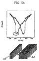
- the resistance variance in the silicon nano spin device means a variance of an electrical signal obtained by injecting an electron spin-polarized at the first ferromagnetic electrode (source) into the silicon, then transporting in the silicon without losing the information, and then detecting from the second electrode (drain) when a magnetic field was applied in a long axis direction of the electrode (that is, a longitudinal direction thereof) and thus to be varied.
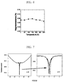
- Figure 6 is a graph showing a relation between a magneto-resistance and a temperature in 4-300K.
- the magneto-resistance according to the temperature was scarcely varied and the magneto-resistance of approximately 0.1% was maintained until the high temperature.
- a spin transistor was illustrated in Figure 9 as one embodiment of the hybrid ferromagnet/ semiconductor device which was fabricated according to the present invention.
- a ferromagnet was used as a source 101 and a drain 102 of the spin transistor.
- a spin-polarized carrier is injected into a channel region 105 from the source 101 and is detected from the drain 102.
- As the channel region a two-dimensional electron gas layer of a compound semiconductor can be used.
- the carrier injected into the channel region can be controlled by using a resistance variance due to an external magnetic field.
- a precession of the spin-polarized carrier which has been injected into the channel region can be controlled by a gate 103.
- a spin-polarized field effect transistor (a spin FET) is implemented.
- Reference numerals 104 and 106 denote a barrier layer (an insulating layer) of a quantum well structure.
Landscapes
- Engineering & Computer Science (AREA)
- Chemical & Material Sciences (AREA)
- Nanotechnology (AREA)
- Power Engineering (AREA)
- Crystallography & Structural Chemistry (AREA)
- Materials Engineering (AREA)
- Manufacturing & Machinery (AREA)
- Physics & Mathematics (AREA)
- Spectroscopy & Molecular Physics (AREA)
- Condensed Matter Physics & Semiconductors (AREA)
- General Physics & Mathematics (AREA)
- Computer Hardware Design (AREA)
- Hall/Mr Elements (AREA)
- Static Random-Access Memory (AREA)
- Thin Magnetic Films (AREA)
- Thin Film Transistor (AREA)
Abstract
Description
| Washing Process of Silicon Wafer | |
| Solvent Removal | |
| 1 | Immerse in boiling trichloroethylene(TCE) for 3 min. |
| 2 | Immerse in boiling acetone for 3 min |
| 3 | Immerse in boiling methyl alcohol for 3 min. |
| 4 | Wash in DI water for 3 min. |
| Heavy Metal Clean | |
| 1 | Immerse in a solution of H2SO4 : H2O2 (4:1) for 10min at a temperature of 120°C. |
| 2 | Quench the solution under running DI water for 1 min. |
| 3 | Wash in running DI water for 10 min. |
| 4 | N2 Blowing. |

Claims (15)
- A hybrid ferromagnet/ semiconductor spin device comprising:a semiconductor substrate;a source region formed on the substrate as a ferromagnet;a spin channel region on the substrate, where a spin-polarized carier at the source region is injected and transported; anda drain region formed on the substrate as a ferromagnet, for detecting a spin which has passed through the spin channel region.
- The hybrid ferromagnet/ semiconductor spin device of claim 1, wherein the ferromagnet is a magnet metal having a great spin polarization, and is one selected from Fe, Co, Ni, FeCo, and NiFe.
- The hybrid ferromagnet/ semiconductor spin device of claim 1, wherein the ferromagnet is one selected from GaMnAs, InMnAs, GeMn, and GaMnN.
- The hybrid ferromagnet/ semiconductor spin device of claim 1, wherein the ferromagnet is a half metal having a spin polarization of 100% such as CrO2.
- The hybrid ferromagnet/ semiconductor spin device of claim 1, wherein the semiconductor is one selected from Si, GaAs, InAs, and Ge.
- The hybrid ferromagnet/ semiconductor spin device of claim 1, wherein the spin channel region is Si on insulator (SOl) or two dimensional electron gas of a compound semiconductor.
- The hybrid ferromagnet/ semiconductor spin device of claim 1, wherein the source region and the drain region have a line width of a range of 5-1000nm.
- The hybrid ferromagnet/ semiconductor spin device of claim 7, wherein an interval between the source region and the drain region is in a range of 10nm-1µm.
- The hybrid ferromagnet/ semiconductor spin device of claim 7, wherein the source region and the drain region have a different line width each other so that a spin switching is anti-parallel in a certain magnet field range.
- The hybrid ferromagnet/ semiconductor spin device of claim 1, wherein a surface of the semiconductor substrate where the source region and the drain region are formed is etched with a depth of a range of 10-500nm.
- The hybrid ferromagnet/ semiconductor spin device of claim 1, wherein a contact resistance between the ferromagnet and the semiconductor is Ohmic or Schottky.
- The hybrid ferromagnet/ semiconductor spin device of claim 1, wherein Al2O3 or AIN is inserted between the ferromagnet and the semiconductor as an intermediate film with a thickness of a range of 0.5-2nm thereby to generate a spin injection by a tunneling.
- A spin-polarized field effect transistor comprising a gate, an insulating layer formed under the gate, a source region and a drain region formed at left and right sides of the insulating layer by using a ferromagnet, and two dimensional electron gas below the insulating layer, wherein a precession of a spin-polarized carrier is controlled by a voltage applied to the gate.
- A fabrication method of a hybrid ferromagnet/ semiconductor spin device comprising the steps of:forming a channel region where a carrier transportation is performed on a semiconductor substrate;etching a surface of the semiconductor substrate of right and left sides of the channel region with a depth of a range of 10-500nm;forming a source region and a drain region with a ferromagnet at the etched regions of the left and right sides of the channel region; andapplying a magnetic field to the ferromagnet source region and the drain region and performing a thermal processing.
- The method of claim 14, wherein the thermal processing is performed by applying a magnetic field of 0.5-5 kOe in a long axis direction of the ferromagnet at a vacuum state with a temperature of 100-500°C for 10-60 minutes.
Applications Claiming Priority (2)
| Application Number | Priority Date | Filing Date | Title |
|---|---|---|---|
| KR2003016170 | 2003-03-14 | ||
| KR10-2003-0016170A KR100511077B1 (en) | 2003-03-14 | 2003-03-14 | Hybrid ferromagnet/semiconductor spin device and fabrication method thereof |
Publications (2)
| Publication Number | Publication Date |
|---|---|
| EP1458031A2 true EP1458031A2 (en) | 2004-09-15 |
| EP1458031A3 EP1458031A3 (en) | 2005-01-26 |
Family
ID=32768650
Family Applications (1)
| Application Number | Title | Priority Date | Filing Date |
|---|---|---|---|
| EP04251433A Withdrawn EP1458031A3 (en) | 2003-03-14 | 2004-03-12 | Hybrid ferromagnet/semiconductor spin device and fabrication method thereof |
Country Status (4)
| Country | Link |
|---|---|
| US (1) | US7084468B2 (en) |
| EP (1) | EP1458031A3 (en) |
| JP (1) | JP2004282067A (en) |
| KR (1) | KR100511077B1 (en) |
Cited By (5)
| Publication number | Priority date | Publication date | Assignee | Title |
|---|---|---|---|---|
| CN100454599C (en) * | 2005-03-31 | 2009-01-21 | 株式会社东芝 | Spin Injection Field Effect Transistors, Magnetic Random Access Memory, and Reconfigurable Logic Circuits |
| US8821837B2 (en) | 2007-07-16 | 2014-09-02 | University Of Central Florida Research Foundation, Inc. | Aqueous method of making magnetic iron oxide nanoparticles |
| US9057094B1 (en) | 2007-10-25 | 2015-06-16 | University Of Central Florida Research Foundation, Inc. | Nanoparticle-mediated methods for antimicrobial susceptibility testing of bacteria |
| US9109249B2 (en) | 2011-05-19 | 2015-08-18 | University Of Central Florida Research Foundation, Inc. | Microbe detection via hybridizing magnetic relaxation nanosensors |
| CN109360853A (en) * | 2018-08-15 | 2019-02-19 | 杭州电子科技大学 | Heterojunction structures and methods for enhancing the spin polarizability of molybdenum disulfide zigzag ribbons |
Families Citing this family (28)
| Publication number | Priority date | Publication date | Assignee | Title |
|---|---|---|---|---|
| KR100681379B1 (en) * | 2003-03-07 | 2007-02-12 | 도꾸리쯔교세이호징 가가꾸 기쥬쯔 신꼬 기꼬 | Field Effect Transistor with Spin-Dependent Transfer Characteristics and Nonvolatile Memory Using the Same |
| JP4469570B2 (en) * | 2003-07-24 | 2010-05-26 | 株式会社東芝 | Magnetoresistive element, magnetic head, and magnetic recording / reproducing apparatus |
| US7099122B2 (en) * | 2003-12-16 | 2006-08-29 | Seagate Technology Llc | Spin polarization enhancement artificial magnet |
| US7411235B2 (en) | 2004-06-16 | 2008-08-12 | Kabushiki Kaisha Toshiba | Spin transistor, programmable logic circuit, and magnetic memory |
| KR100697779B1 (en) * | 2005-03-05 | 2007-03-20 | 한국과학기술연구원 | Hybrid Magnetic / Semiconductor Spin Device Using SOI Substrate and Manufacturing Method Thereof |
| US7956608B1 (en) * | 2005-06-27 | 2011-06-07 | Northwestern University | Method of using group III-V ferromagnetic/non-magnetic semiconductor heterojunctions and magnetodiodes |
| US7655324B2 (en) * | 2005-09-20 | 2010-02-02 | Sridhar Kasichainula | Electro-magnetic storage device and method |
| KR100796281B1 (en) * | 2006-02-28 | 2008-01-21 | 서울시립대학교 산학협력단 | Spin-dependent single electron transistor |
| US20080012004A1 (en) * | 2006-03-17 | 2008-01-17 | Mears Technologies, Inc. | Spintronic devices with constrained spintronic dopant |
| US7625767B2 (en) * | 2006-03-17 | 2009-12-01 | Mears Technologies, Inc. | Methods of making spintronic devices with constrained spintronic dopant |
| US8098515B2 (en) * | 2006-07-07 | 2012-01-17 | The Regents Of The University Of California | Spin injection device having semiconductor-ferromagnetic-semiconductor structure and spin transistor |
| WO2008005719A2 (en) * | 2006-07-07 | 2008-01-10 | The Regents Of The University Of California | Spin injector |
| US7342244B2 (en) * | 2006-07-19 | 2008-03-11 | Tokyo Electron Limited | Spintronic transistor |
| KR100852182B1 (en) * | 2006-08-22 | 2008-08-13 | 한국과학기술연구원 | Hybrid semiconductor-ferromagnet device with a junction of positive and negative magnetic-field regions |
| KR100855105B1 (en) * | 2007-06-14 | 2008-08-29 | 한국과학기술연구원 | Spin Transistor Using Vertical Magnetization |
| KR100953532B1 (en) * | 2007-10-09 | 2010-04-21 | 한국과학기술연구원 | Nanomagnetic / Magnetic Semiconductor Hybrid Spin Device and Manufacturing Method Thereof |
| US20090141409A1 (en) * | 2007-12-03 | 2009-06-04 | Santos Tiffany S | Spin filter spintronic devices |
| KR100852183B1 (en) * | 2008-05-30 | 2008-08-13 | 한국과학기술연구원 | Semiconductor-Magnetic Convergence Device with Negative and Positive Junction Structure in Magnetic Field |
| KR100852184B1 (en) * | 2008-05-30 | 2008-08-13 | 한국과학기술연구원 | Semiconductor-Magnetic Convergence Device with Negative and Positive Junction Structure in Magnetic Field |
| EP2190022B1 (en) * | 2008-11-20 | 2013-01-02 | Hitachi Ltd. | Spin-polarised charge carrier device |
| KR101598542B1 (en) | 2009-01-13 | 2016-02-29 | 삼성전자주식회사 | Logic circuit device using spin field effect transistor |
| JP2010238956A (en) * | 2009-03-31 | 2010-10-21 | Tdk Corp | Spin conductive device |
| JP2010239011A (en) * | 2009-03-31 | 2010-10-21 | Tdk Corp | Spin injection structure and spin conduction device using the same |
| US8766341B2 (en) * | 2009-10-20 | 2014-07-01 | The Regents Of The University Of California | Epitaxial growth of single crystalline MgO on germanium |
| US8692343B2 (en) * | 2010-04-26 | 2014-04-08 | Headway Technologies, Inc. | MR enhancing layer (MREL) for spintronic devices |
| KR101084019B1 (en) | 2010-05-12 | 2011-11-16 | 한국과학기술연구원 | Complementary Spin Transistor Logic Circuit |
| CN102774806A (en) * | 2012-06-25 | 2012-11-14 | 中国科学院上海技术物理研究所 | Producing method of micro-mesa of Mn-Co-Ni-O line array detector |
| CN110190182B (en) * | 2019-05-28 | 2023-07-25 | 衢州学院 | A Design Method for Ultrathin Spin Valve Devices |
Family Cites Families (5)
| Publication number | Priority date | Publication date | Assignee | Title |
|---|---|---|---|---|
| US5465185A (en) * | 1993-10-15 | 1995-11-07 | International Business Machines Corporation | Magnetoresistive spin valve sensor with improved pinned ferromagnetic layer and magnetic recording system using the sensor |
| US5654566A (en) * | 1995-04-21 | 1997-08-05 | Johnson; Mark B. | Magnetic spin injected field effect transistor and method of operation |
| US5962905A (en) * | 1996-09-17 | 1999-10-05 | Kabushiki Kaisha Toshiba | Magnetoresistive element |
| US6069820A (en) * | 1998-02-20 | 2000-05-30 | Kabushiki Kaisha Toshiba | Spin dependent conduction device |
| JP2003248909A (en) * | 2002-02-27 | 2003-09-05 | Hitachi Ltd | Magnetic head, magnetic recording / reproducing apparatus including the same, and magnetic memory |
-
2003
- 2003-03-14 KR KR10-2003-0016170A patent/KR100511077B1/en not_active Expired - Fee Related
-
2004
- 2004-03-11 JP JP2004068644A patent/JP2004282067A/en active Pending
- 2004-03-12 EP EP04251433A patent/EP1458031A3/en not_active Withdrawn
- 2004-03-15 US US10/801,744 patent/US7084468B2/en not_active Expired - Fee Related
Cited By (7)
| Publication number | Priority date | Publication date | Assignee | Title |
|---|---|---|---|---|
| CN100454599C (en) * | 2005-03-31 | 2009-01-21 | 株式会社东芝 | Spin Injection Field Effect Transistors, Magnetic Random Access Memory, and Reconfigurable Logic Circuits |
| US8821837B2 (en) | 2007-07-16 | 2014-09-02 | University Of Central Florida Research Foundation, Inc. | Aqueous method of making magnetic iron oxide nanoparticles |
| US9125941B2 (en) | 2007-07-16 | 2015-09-08 | University Of Central Florida Research Foundation, Inc. | Aqueous method for making magnetic iron oxide nanoparticles |
| US9057094B1 (en) | 2007-10-25 | 2015-06-16 | University Of Central Florida Research Foundation, Inc. | Nanoparticle-mediated methods for antimicrobial susceptibility testing of bacteria |
| US9109249B2 (en) | 2011-05-19 | 2015-08-18 | University Of Central Florida Research Foundation, Inc. | Microbe detection via hybridizing magnetic relaxation nanosensors |
| CN109360853A (en) * | 2018-08-15 | 2019-02-19 | 杭州电子科技大学 | Heterojunction structures and methods for enhancing the spin polarizability of molybdenum disulfide zigzag ribbons |
| CN109360853B (en) * | 2018-08-15 | 2022-01-14 | 杭州电子科技大学 | Heterojunction structure and method for improving spin polarizability of molybdenum disulfide sawtooth-shaped strip |
Also Published As
| Publication number | Publication date |
|---|---|
| KR20040081625A (en) | 2004-09-22 |
| JP2004282067A (en) | 2004-10-07 |
| US20040178460A1 (en) | 2004-09-16 |
| US7084468B2 (en) | 2006-08-01 |
| KR100511077B1 (en) | 2005-08-30 |
| EP1458031A3 (en) | 2005-01-26 |
Similar Documents
| Publication | Publication Date | Title |
|---|---|---|
| US7084468B2 (en) | Hybrid ferromagnet/semiconductor spin device and fabrication method therof | |
| US20110063758A1 (en) | Spin filter junction and method of fabricating the same | |
| US20040052006A1 (en) | Magnetoresistance element and magnetoresistance storage element and magnetic memory | |
| Boeve et al. | Strongly reduced bias dependence in spin–tunnel junctions obtained by ultraviolet light assisted oxidation | |
| AU2009208092A1 (en) | Tunable magnetic switch | |
| JPH11204854A (en) | Magnetic device and magnetic element | |
| KR100650416B1 (en) | Hybrid Magnetic / Semiconductor Nanowire Spin Device and Manufacturing Method Thereof | |
| Boeve et al. | Area scaling of planar ferromagnetic tunnel junctions: From shadow evaporation to lithographic microfabrication | |
| KR100697779B1 (en) | Hybrid Magnetic / Semiconductor Spin Device Using SOI Substrate and Manufacturing Method Thereof | |
| Kumar et al. | The spin-valve transistor1 | |
| Law et al. | Spin transfer torque magnetoresistive random access memory | |
| US20060262593A1 (en) | Magnetic memory composition and method of manufacture | |
| van't Erve | Device properties of the spin-valve transistor and the magnetic tunnel transistor | |
| Gandini | Nanofabrication and characterization of spin orbit logic devices | |
| Butler | Lithographic techniques for fabrication of spin injection and detection devices exploiting ferromagnetic semiconducting Gadolinium Nitride | |
| Luo et al. | Nanoscale Magnetic Tunnel Junctions Fabricated Using Etching-Back Technique | |
| Luongo | Nanoparticle-Based Spintronic Computer Logic Switch | |
| Albert | The fabrication and measurement of current perpendicular to the plane magnetic nanostructures for the study of the spin transfer effect | |
| Ko | Charge transport properties in semiconductor nanowires | |
| Shi | Spin Orbit Torque Driven Magnetic Switching in Three Terminal Magnetic Tunnel Junctions | |
| Kim et al. | Size dependence of the magnetic and electrical properties of the spin-valve transistor | |
| Opondo | Transport studies in the ferromagnetic semiconductor (gallium, manganese) arsenic | |
| Misuraca | Investigation of spin transport and accumulation in aluminum gallium arsenide | |
| THIYAGARAJAH | Physical and Magnetic Properties of [Co/Pd] based Spin-Valves with Perpendicular Anisotropy for Spintronic Device Application | |
| Han et al. | Microfabrication of magnetic tunnel junctions using Al as bottom conduction electrode |
Legal Events
| Date | Code | Title | Description |
|---|---|---|---|
| PUAI | Public reference made under article 153(3) epc to a published international application that has entered the european phase |
Free format text: ORIGINAL CODE: 0009012 |
|
| AK | Designated contracting states |
Kind code of ref document: A2 Designated state(s): AT BE BG CH CY CZ DE DK EE ES FI FR GB GR HU IE IT LI LU MC NL PL PT RO SE SI SK TR |
|
| AX | Request for extension of the european patent |
Extension state: AL HR LT LV MK |
|
| RIN1 | Information on inventor provided before grant (corrected) |
Inventor name: KIM, YOUNG KEUN Inventor name: SHIN, MOO WHAN Inventor name: HWANG, WOONG JUN Inventor name: LEE, HAN JOO Inventor name: KIM, HI JUNG Inventor name: CHANG, JOON YEON Inventor name: HAN, SUK HEE Inventor name: LEE, WOO YOUNG |
|
| PUAL | Search report despatched |
Free format text: ORIGINAL CODE: 0009013 |
|
| RIC1 | Information provided on ipc code assigned before grant |
Ipc: 7H 01L 29/66 B Ipc: 7H 01L 29/86 B Ipc: 7H 01L 29/76 A |
|
| AK | Designated contracting states |
Kind code of ref document: A3 Designated state(s): AT BE BG CH CY CZ DE DK EE ES FI FR GB GR HU IE IT LI LU MC NL PL PT RO SE SI SK TR |
|
| AX | Request for extension of the european patent |
Extension state: AL HR LT LV MK |
|
| 17P | Request for examination filed |
Effective date: 20050303 |
|
| 17Q | First examination report despatched |
Effective date: 20050421 |
|
| AKX | Designation fees paid |
Designated state(s): AT BE BG CH CY CZ DE DK EE ES FI FR GB GR HU IE IT LI LU MC NL PL PT RO SE SI SK TR |
|
| STAA | Information on the status of an ep patent application or granted ep patent |
Free format text: STATUS: THE APPLICATION IS DEEMED TO BE WITHDRAWN |
|
| 18D | Application deemed to be withdrawn |
Effective date: 20060527 |