EP1459363B1 - Verfahren zur nachätz- und beseitigungsrestentfernung an koralfilmen - Google Patents
Verfahren zur nachätz- und beseitigungsrestentfernung an koralfilmen Download PDFInfo
- Publication number
- EP1459363B1 EP1459363B1 EP02797461A EP02797461A EP1459363B1 EP 1459363 B1 EP1459363 B1 EP 1459363B1 EP 02797461 A EP02797461 A EP 02797461A EP 02797461 A EP02797461 A EP 02797461A EP 1459363 B1 EP1459363 B1 EP 1459363B1
- Authority
- EP
- European Patent Office
- Prior art keywords
- cleaning
- low
- semiconductor wafer
- residues
- ashing
- Prior art date
- Legal status (The legal status is an assumption and is not a legal conclusion. Google has not performed a legal analysis and makes no representation as to the accuracy of the status listed.)
- Expired - Lifetime
Links
Images



Classifications
-
- H—ELECTRICITY
- H10—SEMICONDUCTOR DEVICES; ELECTRIC SOLID-STATE DEVICES NOT OTHERWISE PROVIDED FOR
- H10P—GENERIC PROCESSES OR APPARATUS FOR THE MANUFACTURE OR TREATMENT OF DEVICES COVERED BY CLASS H10
- H10P52/00—Grinding, lapping or polishing of wafers, substrates or parts of devices
-
- H—ELECTRICITY
- H10—SEMICONDUCTOR DEVICES; ELECTRIC SOLID-STATE DEVICES NOT OTHERWISE PROVIDED FOR
- H10P—GENERIC PROCESSES OR APPARATUS FOR THE MANUFACTURE OR TREATMENT OF DEVICES COVERED BY CLASS H10
- H10P70/00—Cleaning of wafers, substrates or parts of devices
- H10P70/20—Cleaning during device manufacture
- H10P70/23—Cleaning during device manufacture during, before or after processing of insulating materials
- H10P70/234—Cleaning during device manufacture during, before or after processing of insulating materials the processing being the formation of vias or contact holes
-
- H—ELECTRICITY
- H10—SEMICONDUCTOR DEVICES; ELECTRIC SOLID-STATE DEVICES NOT OTHERWISE PROVIDED FOR
- H10P—GENERIC PROCESSES OR APPARATUS FOR THE MANUFACTURE OR TREATMENT OF DEVICES COVERED BY CLASS H10
- H10P50/00—Etching of wafers, substrates or parts of devices
- H10P50/20—Dry etching; Plasma etching; Reactive-ion etching
- H10P50/24—Dry etching; Plasma etching; Reactive-ion etching of semiconductor materials
- H10P50/242—Dry etching; Plasma etching; Reactive-ion etching of semiconductor materials of Group IV materials
-
- H—ELECTRICITY
- H10—SEMICONDUCTOR DEVICES; ELECTRIC SOLID-STATE DEVICES NOT OTHERWISE PROVIDED FOR
- H10W—GENERIC PACKAGES, INTERCONNECTIONS, CONNECTORS OR OTHER CONSTRUCTIONAL DETAILS OF DEVICES COVERED BY CLASS H10
- H10W20/00—Interconnections in chips, wafers or substrates
- H10W20/01—Manufacture or treatment
- H10W20/071—Manufacture or treatment of dielectric parts thereof
- H10W20/081—Manufacture or treatment of dielectric parts thereof by forming openings in the dielectric parts
-
- H—ELECTRICITY
- H10—SEMICONDUCTOR DEVICES; ELECTRIC SOLID-STATE DEVICES NOT OTHERWISE PROVIDED FOR
- H10P—GENERIC PROCESSES OR APPARATUS FOR THE MANUFACTURE OR TREATMENT OF DEVICES COVERED BY CLASS H10
- H10P72/00—Handling or holding of wafers, substrates or devices during manufacture or treatment thereof
- H10P72/04—Apparatus for manufacture or treatment
- H10P72/0402—Apparatus for fluid treatment
- H10P72/0406—Apparatus for fluid treatment for cleaning followed by drying, rinsing, stripping, blasting or the like
- H10P72/0411—Apparatus for fluid treatment for cleaning followed by drying, rinsing, stripping, blasting or the like for wet cleaning or washing
- H10P72/0412—Apparatus for fluid treatment for cleaning followed by drying, rinsing, stripping, blasting or the like for wet cleaning or washing using mainly scrubbing means, e.g. brushes
-
- Y—GENERAL TAGGING OF NEW TECHNOLOGICAL DEVELOPMENTS; GENERAL TAGGING OF CROSS-SECTIONAL TECHNOLOGIES SPANNING OVER SEVERAL SECTIONS OF THE IPC; TECHNICAL SUBJECTS COVERED BY FORMER USPC CROSS-REFERENCE ART COLLECTIONS [XRACs] AND DIGESTS
- Y10—TECHNICAL SUBJECTS COVERED BY FORMER USPC
- Y10S—TECHNICAL SUBJECTS COVERED BY FORMER USPC CROSS-REFERENCE ART COLLECTIONS [XRACs] AND DIGESTS
- Y10S438/00—Semiconductor device manufacturing: process
- Y10S438/906—Cleaning of wafer as interim step
Definitions
- This invention relates generally to substrate fabrication, and more particularly to semiconductor wafer cleaning after etch operations.
- semiconductor devices are fabricated from semiconductor wafers, which are subjected to numerous processing operations. These operations include, for example, impurity implants, gate oxide generation, inter-metal low K dielectric, metallization depositions, photolithography pattering, etching operations, chemical mechanical polishing (CMP), etc.
- CMP chemical mechanical polishing
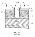
- Figure 1A illustrates a cross-section partial view of a layer stack, representing the layers formed during the fabrication of a typical semiconductor integrated circuit (IC) device.
- the layer stack typically can have numerous layers in the stack. Only a top portion of the stack where processing is taking place is shown.
- Metallization layer 13 typically includes aluminum, copper or one or more of a variety of known aluminum alloys such as Al--Cu, Al--Si, and Al--Cu--Si.
- ARC anti-reflective coating
- ARC layer 14 is typically composed of Ti, TiN or TiW.
- ARC layer 14 is useful in preventing light used in photolithography processes from reflecting and scattering off of the metallization layer 13 surface.
- a low K dielectric layer 16 is then formed over the ARC layer 14.
- a photoresist layer 18 is then spin coated over the low K dielectric layer 16 and patterned to define windows where etching is desired.
- photoresist layer 18 represents a layer of conventional photo-sensitive resist material that may be patterned using patterned reticles and a stepper that passes selective light waves onto the surface of photoresist layer 18.
- the layers of the layer stack are readily recognizable to those skilled in the art and may be formed using any number of known deposition processes, including chemical vapor deposition (CVD), plasma-enhanced chemical vapor deposition (PECVD), physical vapor deposition (PVD) such as sputtering, spin coating, etc.
- CVD chemical vapor deposition
- PECVD plasma-enhanced chemical vapor deposition
- PVD physical vapor deposition
- an etch operation 20 is performed in order to selectively remove portions of the low K dielectric layer 16.
- a feature 17 is etched into the low K dielectric layer 16, and the feature 17 may be a trench, a via hole, or any other geometric pattern.
- the etch 20 is chosen to have good selectivity to enable efficient etching of the low K dielectric 16 layer.
- polymer formation 22 is known to occur on the sidewalls of features 17 being etched.
- Figure 1B shows the a cross-section view of a layer stack after an ashing operation 23 is conducted after the plasma etching operation.
- the ashing operation serves to remove the photoresist layer 18.
- Residue 27 is left after the ashing operation 23.
- Residue 27 may include both etching residues and ashing residues.
- the actual composition of the residue 27 depends upon the material being etched, the chemistry used for the etching, the chemistries used for ashing, and the underlying material.
- the material representing the residue 27 will generally be a low K dielectric material containing some of the etch chemistry components, ashing chemistry components, carbon from the photoresist, and organic residues.
- the residue 27 may extend along the sidewalls and up onto the photoresist layer 18.
- a residue crown 27' may form on the surface of the low K dielectric layer.
- the present invention tills these needs by providing an improved method for cleaning low K dielectric features after etching and ashing in a wafer processing operation. It should be appreciated that the present invention can be implemented in numerous ways, including as a process, or a system. Several inventive embodiments of the present invention are described below.
- a method for cleaning a semiconductor wafer comprising:
- a system for cleaning a semiconductor wafer comprising:
- a system is understood as including the machine to carry out the method, the necessary chemicals and the semiconductor water with etched low K dielectric layer.
- the advantages of the present invention are numerous. Most notably, by utilizing a method for optimized mechanical and chemical cleaning of a low K dielectric features after an etching and ashing processes, contaminating residues which may form crowns or other contaminating accumulations can be removed in an efficient manner. Specifically, mechanical brushing and use of a fluid mixture with a cleaning chemistry and a wetting agent may advantageously remove contaminating residues from the low K dielectric features and the surface of the low K dielectric layer. Therefore, when low K dielectric materials such as CoralTM is utilized, the fluid mixture in conjunction with brush scrubbing may clean CoraTM films and CoralTM contaminants in an substantially enhanced manner.
- low K dielectric materials such as CoralTM
- the present invention fills these needs by providing a method for efficiently cleaning post etch and post ashing residues when a low K dielectric features is formed in a semiconductor wafer.
- numerous specific details are set forth in order to provide a thorough understanding of the present invention. It will be understood, however, by one of ordinary skill in the art, that the present invention may be practiced without some or all of these specific details.
- well known process operations have not been described in detail in order not to unnecessarily obscure the present invention. It will be obvious, however, to one skilled in the art, that the present invention may be practiced without some or all of these specific details. In other instances, well known process operations have not been described in detail in order not to unnecessarily obscure the present invention.
- an invention for a method of efficiently cleaning etched features of given layers of a semiconductor wafer.
- the cleaning is designed to efficiently remove post plasma etch and post ashing residues and other particulates from in and around etched low K dielectric features.
- the low K dielectric material is typically engineered to have a dielectric constant ranging between about 1.5 and about 3.5 while silicon dioxide typically has a dielectric constant of about 4.0.
- CoralTM has a dielectric constant value of between about 2.5 to about 2.8.
- the low K dielectric polymer material is a much better insulator than the silicon dioxide dielectric materials, and greatly reduces the coupling capacitance between metal lines, it is much harder to clean and remove particles and/or metal contaminants from the surface of the a low K dielectric layer because it is hydrophobic. Consequently, conventional water and other aqueous cleaning fluids are unable to wet the surface and rinse away particle contaminants because they are repelled and bead on the surface of the low dielectric layer.
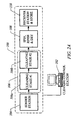
- FIG. 2A shows a wafer cleaning station 100 for use in cleaning low K dielectric features that may be controlled in an automated way by a cleaning control station 102 in accordance with one embodiment of the present invention.
- the wafer cleaning station 100 includes a sender station 104, a cleaning stage 106, a spin-rinse and dry (SRD) station 108, and a receiver station 110.
- SRD spin-rinse and dry
- cleaning systems can be used to carry out different kinds of substrate preparation operations, such as, cleaning, etching, buffing, and the like.
- semiconductor wafers are initially placed into the sender station 104.
- the sender station 104 then delivers wafers (one-at-a-time) to the cleaning stage 106.
- the cleaning stage 106 is divided into a first cleaning stage 106a and a second cleaning stage 106b, although having just one cleaning stage 106 will also work.
- the wafer After passing through the cleaning stage 106, the wafer is passed through an exit spray in order to remove the cleaning fluids and any contaminants.
- the SRD station 108 dries the wafer and then it is delivered to the receiver station 110 for temporary storage.
- FIG. 2B shows a more detailed schematic of an exemplary wafer cleaning station 100 in accordance with one embodiment of the present invention.
- Both the sender station 104 and the receiving station 110 are preferably adapted to receive a cassette containing a number of wafers.
- the first and second cleaning stages 106a and 106b preferably include a set of polyvinyl alcohol (PVA) brushes 120 that have through the brush cleaning fluid application, although fluid can be applied to the brush through the drip manifold.
- PVA polyvinyl alcohol
- Figure 3A illustrates a simplified three-dimensional diagram of a pair of brushes 120a and 120b for scrubbing a top surface and a bottom surface, respectively, of a wafer 130.
- the wafer 130 is caused to rotate in a particular direction while the brushes 120 rotate around an axis of rotation and the surface of the brushes 120 are in contact with the surfaces of the wafer 130.
- the brushes 120a and 120b are mounted on brush cores 200a and 200b.
- the brush cores 200 are configured to have a shaft 201 which has a fluid inlet 202.
- the fluid inlet 202 will thus supply the desired fluids into the brush cores 200.
- the brush cores 200 preferably have a plurality of holes that will allow the fluids to uniformly exit the brush core 200 and evenly supply the desired fluid to the brush 120.
- the desired fluid utilized in cleaning low K dielectric features such as, for example, CoralTM features may be a mixture of a cleaning chemistry and a wetting agent.
- the cleaning chemistry may be any suitable combination of chemicals that may enhance cleaning of contaminants such as, for example ammonia, deionized water, or SC-1 solution.
- the cleaning chemistry is a standard clean-1 (SC-1) solution mixed with a surfactant.
- SC-1 solution is a combination of NH 4 OH, H 2 O 2 , and deionized (DI) water.
- the SC-1 solution for use with a surfactant for cleaning low K dielectric features has a concentration of between about 1 part NH 4 OH, 4 parts H 2 O 2 30 parts deionized (DI) water and about 1 part NH 4 OH, 4 parts H 2 O 2 , 10 parts deionized (DI) water, and preferably about 1 part NH 4 OH, 4 parts H 2 O 2 20 parts deionized (DI) water.
- the wetting agent may any suitable chemical or a combination of chemicals that may render hydrophobic substances cleanable by the cleaning chemistry.
- the wetting agent is a surfactant such as, for example, hydrocarbon surfactants or fluorinated surfactants.
- the surfactant utilized may be fluorinated surfactants made by 3M of St. Paul, Minnesota. Fluorinated surfactants dramatically lower surface tension values at extremely low concentrations when compared to conventional surfactants. Examples of fluorinated surfactants made by 3M include anionic surfactants, such as FC-93, amphoteric surfactants, such as FC-100, FC-120, cationic surfactants, such as FC-135, and nonionic surfactants, such as FC-171.
- FC-120 is a preferred choice but others will work as well.
- Surfactants may provide additional cleaning abilities to the SC-1 solution because low K dielectrics such as, for example, CoralTM is generally a hydrophobic compound.
- Surfactant molecules are amphiphilic, containing both hydrophobic and hydrophilic groups (e.g., a hydrophilic group and a hydrophobic group). Thus, the hydrophobic group of the surfactant molecule is attracted to a hydrophobic surface. When surfactant is applied to the wafer, the hydrophobic group attaches the surfactant molecule to the low K dielectric polymer material.
- the hydrophilic group of the surfactant molecule attracts SC-1 solution to enable the wetting of the surface of the low K dielectric layer. Because the surface now wets, the contaminants in the low K dielectric features may be removed through the chemical cleaning. In addition, the top and bottom brushes 120a and 120b remove the particle and metal contaminants and sweep them into the cleaning fluids by scrubbing the low K dielectric layer. Therefore, by use of surfactants with the SC-1 solution, hydrophobic materials may be made wettable so both hydrophilic and hydrophobic materials can be cleaned away by the chemicals of the SC-1 solution.
- the SC-1 cleaning solution may be premixed with the surfactant so the fluid mixture that enters the brush cores 200 is the SC-1/surfactant cleaning solution. Therefore, the fluid mixture can be applied through the plurality of holes from the brush core 200 of the brushes 200. In this manner, the wafer with the low K dielectric features may be cleaned with a combination of mechanical energy and chemical removal.
- Figures 3B and 3C illustrate cross-sectional views of two different orientations for scrubbing a wafer 130, in accordance with one embodiment of the present invention.
- the wafer is held horizontally while a top brush 120a scrubs the top surface of the wafer 130, and a bottom brush 120b scrubs the bottom surface of the wafer 130.
- the wafer 130 is configured to rotate (using rollers not shown) at the same time that the brushes 120 rotate to ensure that the entire surface area of the wafer is properly scrubbed to remove contaminants, etch the surface to a desired degree, or buff the surface.
- Figure 3B illustrates a horizontal wafer scrubber 100b.
- Figure 3C illustrates a vertical wafer scrubber 100c in which the wafer 130 is scrubbed while in a vertical position.
- the wafer 130 sits on a pair of rollers of the scrubber 100c.
- the brushes 120 are configured to rotate in a desired direction such that both sides of the wafer 130 are evenly scrubbed, using an equal and opposite pressure on each side of the wafer 130.
- FIG 4 shows a flowchart 200 that illustrates a method for etching and cleaning low K dielectric features in accordance with one embodiment of the present invention.
- the method begins with operation 202 where a photoresist patterned low K dielectric layer of a semiconductor wafer is provided where the low K dielectric is hydrophobic.
- a semiconductor wafer may have a plurality of layers fabricated thereon, and the photoresist layer is used to pattern a desired layer.
- the layer requiring patterning is a low K dielectric layer.
- any suitable type of low K dielectric material may be utilized such as, for example, low K OSG, Black Diamond TM , HSQ, etc.
- CoralTM made by Novellus Systems, Inc., in San Jose, California, may be used as the low K dielectric layer.
- the method moves to operation 204 where a plasma etch operation is performed to etch the low K dielectric layer where the plasma etch generates residues.
- the plasma etching may be used to perform via hole etching, contact hole etching, trenches, and other features in the low K dielectric layer.
- Operation 204 typically generates etching residues (as can be seen in Figure 1 ) on the etched features.
- the etching residues may include a composition of the plasma etching chemistries, carbon from photoresist material, the low K dielectric layer being etched, and components from the material that underlies the low K dielectric layer being etched.
- the method moves to operation 206 which performs an ashing operation to remove the photoresist where the ashing operation leaves some ashing residues
- the method utilizes ashing operations well known to one skilled in the art that are commonly used to remove photoresist materials.
- operation 208 which performs a brush scrubbing operation using a fluid mixture including a cleaning chemistry and a wetting agent to remove residues from the low K dielectric layer.
- the wafer is processed through a brush scrubbing system with the cleaning chemistry and the wetting agent.
- the cleaning chemistry may be an SC-1 solution and the wetting agent may be a surfactant.
- the brush scrubbing operation can be performed in a brush scrubbing station that incorporates a pair of brushes for evenly brushing each side of the processed semiconductor wafer. Operation 208 is discussed in further detail in reference to Figure 5 .
- Figure 5 illustrates a flow chart 208 defining the performance of a brush scrubbing operation with cleaning chemistry and a wetting agent to remove the generated low K dielectric etch residues and ashing residues in accordance with one embodiment of the present invention.
- the flow chart 208 begins with operation 240 where the cleaning chemistry and the surfactant is premixed.
- the cleaning chemistry and the surfactant may be those as described in reference to Figure 3A .
- operation 242 applies the premixed chemistry to a brush in a first brush box.
- the brushing operation is designed to be performed by supplying the premixed chemistry through the brush (TTB) for application of the premixed chemistry to the surface of the wafer.
- TTB brush
- other suitable ways to apply the premixed chemistry to the brush such as also described in operation 248 below in reference to a brush in a second brush box
- two brushes may be utilized in the first brush box and second brush box to clean both sides of the wafer.
- the premixed chemistry is supplied to a brush core from which the premixed chemistry is supplied to the surface of the brush through a plurality of holes.
- the method moves to operation 244 which applies the brush in the first brush box to a wafer.
- the application of the brush to the wafer enables the scrubbing of the surface for a period of, in one embodiment, between about 15 seconds and about 60 seconds, and preferably around 35 seconds.
- the premixed chemistry may be continuously supplied to the brush during the scrubbing process.
- the pH of the brush is kept constant where the pH of the is between about 9 and about 13. It should be noted that brush scrub cleaning in the context of post etch and ashing operations of low K dielectric features is substantially different that the conventional technique of chemical bath treatment or chemical spray treatment. Therefore, by using both the premixed chemistry for chemical cleaning and mechanical scrubbing by the brush, residues (e.g. the etching residues and the ashing residues) on both the surface of the wafer and within the low K dielectric features may be effectively cleaned.
- residues e.g. the etching residues and the ashing residues
- the method advances to operation 246 which moves the wafer from the first brush box to a second brush box.
- operation 246 scrubbing in the first brush box is stopped and the wafer is transported to the second brush box for further wafer cleaning.
- the method progresses to operation 248 where the premixed chemistry is applied to a brush in the second brush box.
- Application of the premixed chemistry to the brush may keep the brush from becoming loaded with contaminants (e.g., etching and ashing residues).
- the same premixed chemistry as utilized in the first brush box may be applied, in one embodiment, TTB to the second brush.
- the method moves to operation 249 which applies the brush in the second brush box to a wafer.
- the brush may scrub for any suitable period of time.
- the brush may scrub the wafer between about 2 and 20 seconds, and preferably 5 seconds.
- the premixed chemistry may be continuously supplied to the brush.
- operation 250 applies deionized (DI) water to the wafer through the brush in the second brush box.
- Operation 250 removes the premixed chemistry and any remaining contaminants from the wafer.
- DI water application to the wafer may progress for any suitable period of time.
- the DI water is applied to the wafer through the brush between about 20 seconds to about 50 seconds, and preferably about 30 seconds.
- Any suitable DI water flow rate may be utilized in operation 250.
- the flow rate of DI water is between about 1200 ml per minute to about 3500 ml per minute, and preferably about 3000 ml per minute.
- DI water may be applied to the wafer through a separate set of rinse nozzles.
- the brush scrubbing operation that includes the delivery of chemicals followed by a DI water rinse is configured to yield a high degree of cleanliness while removing the generated etch residues and ashing residues from within the etched low K dielectric features, as well as removing other particulates and contaminants that may have been deposited during the ashing operation.
- operation 252 dries the wafer and delivers a wafer to a receiver station for temporary storage.
Landscapes
- Cleaning Or Drying Semiconductors (AREA)
Claims (14)
- Ein Verfahren zum Reinigen eines Halbleiter-Wafers, aufweisend:Plasmaätzen eines Merkmals (feature) in eine dielektrische Schicht mit niedrigem K-Wert mit einer Fotolackmaske, wobei das Plasmaätzen Ätzrückstände erzeugt,Veraschen des Haltleiter-Wafers zum Entfernen der Fotolackmaske, wobei das Veraschen Veraschungsrücksstände erzeugt, undEntfernen der Ätzrückstände und der Veraschungsrückstände von der dielektrischen Schicht mit geringem K-Wert, wobei das Entfernen verbessert wird durch ein Schrubben der dielektrischen Schicht mit geringem K-Wert des Halbleiter-Wafers mit einer nassen Bürste, die eine Fluid-Mischung aufbringt, die eine Reinigungschemikalie und ein Netzmittel enthält,
wobei das Netzmittel ein Tensid ist und die Reinigungschemikalie eine Kombination von NH4OH, H2O2 und entionisiertem Wasser umfasst. - Ein Verfahren zum Reinigen eines Halbleiter-Wafers nach Anspruch 1, wobei das Tensid ausgewählt ist aus einer Gruppe aufweisend Fluortenside und Hydrocarbontenside.
- Ein Verfahren zum Reinigen eines Halbleiter-Wafers nach Anspruch 2, wobei das Tensid eine Konzentration zwischen ungefähr 0,005 Gew.-% und 0,1 Gew.-% aufweist.
- Ein Verfahren zum Reinigen eines Halbleiter-Wafers nach Anspruch 2, wobei das Tensid eine Konzentration von ungefähr 0,01 Gew.-% aufweist.
- ein Verfahren zum Reinigen eines Halbleiter-Wafers nach Anspruch 1, wobei das Verhältnis der Kombination von NH4OH, H2O2 und entionisiertem Wasser zwischen ungefähr 1:4:10 und ungefähr 1:4:30 ist.
- Ein Verfahren zum Reinigen eines Halbleiter-Wafers nach Anspruch 5, wobei das Verhältnis der Kombination von NH4OH, H2O2 und entionisiertem Wasser ungefähr 1:4:20 ist.
- Ein Verfahren zum Reinigen eins Halbleiter-Wafers nach Anspruch 1, ferner aufweisend:Schrubben der dielektrischen Schicht mit geringem K-Wert unter Verwendung der Bürste während entionisiertes (DI) Wasser aufgebracht wird nach dem Entfernen der Ätzrückstände und der Veraschungsrückstände.
- Ein System zum Reinigen eines Halbleiter-Wafers, aufweisend:Mittel zum Plasmaätzen eines Merkmals (feature) in eine dielektrische Schicht mit geringem K-Wert mit einer Fotolackmaske, wobei das Plasmaätzen Ätzrückstände in und um das Merkmal erzeugt;Mittel zum Aussetzen des Halbleiter-Wafers einem Veraschungsarbeitsschritt zum Entfernen der Fotolackmaske, wobei der Veraschungs-Arbeitsschritt Veraschungsrückstände erzeugt; undMittel zum Schrubben der dielektrischen Schicht mit geringem K-Wert mit einer Bürste, während eine Fluid-Mischung verwendet wird, wobei diese eine Reinigungschemikalie und ein Netzmittel enthält, wobei das Netzmittel ausgewählt ist, die dielektrische Schicht mit geringem K-Wert aufzubereiten, um das Reinigen der Ätzrückstände und der Veraschungsrückstände mit der Reinigungschemikalie zu vereinfachen, wobei das Netzmittel ein Tensid ist und die Reinigungschemikalie eine Kombination von NH4OH, H2O2 und entionisiertem (DI) Wasser umfasst.
- Das System zum Reinigen eines Halbleiter-Wafers nach Anspruch 8, ferner aufweisend:Mittel zum Schrubben der dielektrischen Schicht mit geringem K-Wert unter Verwendung der Bürste während entionisiertes (DI) Wasser aufgebracht wird nach dem Entfernen der Ätzrückstände und der Veraschungsrückstände.
- Das System zum Reinigen eines Halbleiter-Wafers nach Anspruch 8, wobei das Tensid ausgewählt ist aus einer Gruppe, umfassend fluorierte Tenside und Hydrocarbontenside.
- Das System zum Reinigen eines Halbleiter-Wafers nach Anspruch 8, wobei das Tensid eine Konzentration zwischen ungefähr 0,005 Gew.-% und ungefähr 0,1 Gew.-% aufweist.
- Das System zum Reinigen eines Halbleiter-Wafers nach Anspruch 8, wobei das Tensid eine Konzentration von ungefähr 0,01 Gew.-% aufweist.
- Das System zum Reinigen eines Halbleiter-Wafers nach Anspruch 8, wobei das Verhältnis der Kombination von NH4OH, H2O2 und DI-Wasser zwischen ungefähr 1:4:10 und ungefähr 1:4:30 ist.
- Das System zum Reinigen eines Halbleiter-Wafers nach Anspruch 8, wobei das Verhältnis der Kombination von NH4OH, H2O2 und DI-Wasser ungefähr 1:4:20 ist.
Applications Claiming Priority (3)
| Application Number | Priority Date | Filing Date | Title |
|---|---|---|---|
| US33644 | 2001-12-27 | ||
| US10/033,644 US6949411B1 (en) | 2001-12-27 | 2001-12-27 | Method for post-etch and strip residue removal on coral films |
| PCT/US2002/040987 WO2003058694A1 (en) | 2001-12-27 | 2002-12-20 | Method for post-etch and strip residue removal on coral films |
Publications (3)
| Publication Number | Publication Date |
|---|---|
| EP1459363A1 EP1459363A1 (de) | 2004-09-22 |
| EP1459363A4 EP1459363A4 (de) | 2007-08-01 |
| EP1459363B1 true EP1459363B1 (de) | 2010-08-11 |
Family
ID=21871596
Family Applications (1)
| Application Number | Title | Priority Date | Filing Date |
|---|---|---|---|
| EP02797461A Expired - Lifetime EP1459363B1 (de) | 2001-12-27 | 2002-12-20 | Verfahren zur nachätz- und beseitigungsrestentfernung an koralfilmen |
Country Status (9)
| Country | Link |
|---|---|
| US (1) | US6949411B1 (de) |
| EP (1) | EP1459363B1 (de) |
| JP (1) | JP4317759B2 (de) |
| KR (1) | KR100977104B1 (de) |
| CN (1) | CN100392814C (de) |
| AU (1) | AU2002361829A1 (de) |
| DE (1) | DE60237310D1 (de) |
| TW (1) | TWI310403B (de) |
| WO (1) | WO2003058694A1 (de) |
Families Citing this family (10)
| Publication number | Priority date | Publication date | Assignee | Title |
|---|---|---|---|---|
| US7067016B1 (en) * | 2003-03-31 | 2006-06-27 | Lam Research Corporation | Chemically assisted mechanical cleaning of MRAM structures |
| US6936540B2 (en) * | 2003-09-18 | 2005-08-30 | Micron Technology, Inc. | Method of polishing a semiconductor substrate, post-CMP cleaning process, and method of cleaning residue from registration alignment markings |
| KR100720481B1 (ko) * | 2005-11-28 | 2007-05-22 | 동부일렉트로닉스 주식회사 | 반도체 소자의 제조 방법 |
| US7807219B2 (en) * | 2006-06-27 | 2010-10-05 | Lam Research Corporation | Repairing and restoring strength of etch-damaged low-k dielectric materials |
| JP2008060238A (ja) * | 2006-08-30 | 2008-03-13 | Toshiba Corp | 半導体装置の製造方法 |
| CN101622376B (zh) * | 2007-01-30 | 2012-04-04 | 朗姆研究公司 | 使用超临界溶剂在半导体基片上形成金属膜的组合物和方法 |
| US8617301B2 (en) * | 2007-01-30 | 2013-12-31 | Lam Research Corporation | Compositions and methods for forming and depositing metal films on semiconductor substrates using supercritical solvents |
| CN103050374B (zh) * | 2011-10-17 | 2015-11-25 | 中芯国际集成电路制造(北京)有限公司 | 蚀刻后的处理方法 |
| CN108054083A (zh) * | 2017-12-13 | 2018-05-18 | 武汉新芯集成电路制造有限公司 | 一种对晶圆表面颗粒物进行去除的方法 |
| CN111755319A (zh) * | 2019-03-29 | 2020-10-09 | 中芯集成电路(宁波)有限公司 | 晶圆清洗方法及光刻胶图案化方法 |
Family Cites Families (19)
| Publication number | Priority date | Publication date | Assignee | Title |
|---|---|---|---|---|
| JP3217116B2 (ja) * | 1992-03-06 | 2001-10-09 | 日産化学工業株式会社 | 低表面張力洗浄用組成物 |
| JPH07115078A (ja) * | 1993-10-19 | 1995-05-02 | Shimada Phys & Chem Ind Co Ltd | 基板の処理方法およびその装置 |
| JP3326642B2 (ja) | 1993-11-09 | 2002-09-24 | ソニー株式会社 | 基板の研磨後処理方法およびこれに用いる研磨装置 |
| US5413952A (en) * | 1994-02-02 | 1995-05-09 | Motorola, Inc. | Direct wafer bonded structure method of making |
| WO1997013590A1 (en) | 1995-10-13 | 1997-04-17 | Ontrak Systems, Inc. | Method and apparatus for chemical delivery through the brush |
| US5575706A (en) | 1996-01-11 | 1996-11-19 | Taiwan Semiconductor Manufacturing Company Ltd. | Chemical/mechanical planarization (CMP) apparatus and polish method |
| US6277203B1 (en) | 1998-09-29 | 2001-08-21 | Lam Research Corporation | Method and apparatus for cleaning low K dielectric and metal wafer surfaces |
| US6218290B1 (en) * | 1998-11-25 | 2001-04-17 | Advanced Micro Devices, Inc. | Copper dendrite prevention by chemical removal of dielectric |
| US6130167A (en) * | 1999-03-18 | 2000-10-10 | Taiwan Semiconductor Manufacturing Company | Method of preventing corrosion of a metal structure exposed in a non-fully landed via |
| JP4094174B2 (ja) * | 1999-06-04 | 2008-06-04 | 株式会社ルネサステクノロジ | 半導体装置の製造方法 |
| US6274478B1 (en) * | 1999-07-13 | 2001-08-14 | Motorola, Inc. | Method for forming a copper interconnect using a multi-platen chemical mechanical polishing (CMP) process |
| JP4554011B2 (ja) * | 1999-08-10 | 2010-09-29 | ルネサスエレクトロニクス株式会社 | 半導体集積回路装置の製造方法 |
| US6623579B1 (en) * | 1999-11-02 | 2003-09-23 | Alien Technology Corporation | Methods and apparatus for fluidic self assembly |
| US6187684B1 (en) | 1999-12-09 | 2001-02-13 | Lam Research Corporation | Methods for cleaning substrate surfaces after etch operations |
| US6315637B1 (en) * | 2000-01-18 | 2001-11-13 | Advanced Micro Devices, Inc. | Photoresist removal using a polishing tool |
| US6482678B1 (en) * | 2000-03-31 | 2002-11-19 | Lam Research Corporation | Wafer preparation systems and methods for preparing wafers |
| JP4057762B2 (ja) * | 2000-04-25 | 2008-03-05 | 株式会社ルネサステクノロジ | 半導体装置の製造方法 |
| KR100404560B1 (ko) * | 2001-01-06 | 2003-11-05 | 삼성전자주식회사 | 반도체 장치의 제조방법 |
| US20020105057A1 (en) * | 2001-02-02 | 2002-08-08 | Vyvoda Michael A. | Wafer surface that facilitates particle removal |
-
2001
- 2001-12-27 US US10/033,644 patent/US6949411B1/en not_active Expired - Fee Related
-
2002
- 2002-12-18 TW TW091136604A patent/TWI310403B/zh not_active IP Right Cessation
- 2002-12-20 WO PCT/US2002/040987 patent/WO2003058694A1/en not_active Ceased
- 2002-12-20 AU AU2002361829A patent/AU2002361829A1/en not_active Abandoned
- 2002-12-20 EP EP02797461A patent/EP1459363B1/de not_active Expired - Lifetime
- 2002-12-20 JP JP2003558912A patent/JP4317759B2/ja not_active Expired - Fee Related
- 2002-12-20 DE DE60237310T patent/DE60237310D1/de not_active Expired - Lifetime
- 2002-12-20 KR KR1020047010160A patent/KR100977104B1/ko not_active Expired - Fee Related
- 2002-12-20 CN CNB028262689A patent/CN100392814C/zh not_active Expired - Fee Related
Also Published As
| Publication number | Publication date |
|---|---|
| US6949411B1 (en) | 2005-09-27 |
| JP2006502559A (ja) | 2006-01-19 |
| KR100977104B1 (ko) | 2010-08-23 |
| AU2002361829A1 (en) | 2003-07-24 |
| TW200302271A (en) | 2003-08-01 |
| CN1608311A (zh) | 2005-04-20 |
| DE60237310D1 (de) | 2010-09-23 |
| CN100392814C (zh) | 2008-06-04 |
| WO2003058694A1 (en) | 2003-07-17 |
| EP1459363A4 (de) | 2007-08-01 |
| EP1459363A1 (de) | 2004-09-22 |
| JP4317759B2 (ja) | 2009-08-19 |
| KR20040065312A (ko) | 2004-07-21 |
| TWI310403B (en) | 2009-06-01 |
Similar Documents
| Publication | Publication Date | Title |
|---|---|---|
| EP1107301B1 (de) | Verfahren zur Reinigung von Substratoberflächen nach einer Ätzstufe | |
| US7718009B2 (en) | Cleaning submicron structures on a semiconductor wafer surface | |
| US6733596B1 (en) | Substrate cleaning brush preparation sequence, method, and system | |
| US5723019A (en) | Drip chemical delivery method and apparatus | |
| JP4709346B2 (ja) | ウェーハエッジの洗浄装置 | |
| KR100335450B1 (ko) | 반도체 장치의 세정 장비 및 반도체 장치의 세정 방법 | |
| US20090056744A1 (en) | Wafer cleaning compositions and methods | |
| KR101376897B1 (ko) | 액체 메니스커스를 이용한 포스트 에칭 웨이퍼 표면 세정 | |
| US6921494B2 (en) | Backside etching in a scrubber | |
| US6277203B1 (en) | Method and apparatus for cleaning low K dielectric and metal wafer surfaces | |
| US6949411B1 (en) | Method for post-etch and strip residue removal on coral films | |
| US7023099B2 (en) | Wafer cleaning method and resulting wafer | |
| US7067015B2 (en) | Modified clean chemistry and megasonic nozzle for removing backside CMP slurries | |
| US8375965B2 (en) | Systems and methods for single integrated substrate cleaning and rinsing | |
| KR20120108063A (ko) | 호환성 화학물을 이용하는 기판 브러시 스크러빙과 근접 세정-건조 시퀀스, 근접 기판 준비 시퀀스, 및 이를 구현하기 위한 방법, 장치, 및 시스템 | |
| US20080163905A1 (en) | Two step process for post ash cleaning for Cu/low-k dual damascene structure with metal hard mask |
Legal Events
| Date | Code | Title | Description |
|---|---|---|---|
| PUAI | Public reference made under article 153(3) epc to a published international application that has entered the european phase |
Free format text: ORIGINAL CODE: 0009012 |
|
| 17P | Request for examination filed |
Effective date: 20040622 |
|
| AK | Designated contracting states |
Kind code of ref document: A1 Designated state(s): AT BE BG CH CY CZ DE DK EE ES FI FR GB GR IE IT LI LU MC NL PT SE SI SK TR |
|
| AX | Request for extension of the european patent |
Extension state: AL LT LV MK RO |
|
| A4 | Supplementary search report drawn up and despatched |
Effective date: 20070629 |
|
| 17Q | First examination report despatched |
Effective date: 20090218 |
|
| GRAP | Despatch of communication of intention to grant a patent |
Free format text: ORIGINAL CODE: EPIDOSNIGR1 |
|
| GRAS | Grant fee paid |
Free format text: ORIGINAL CODE: EPIDOSNIGR3 |
|
| GRAA | (expected) grant |
Free format text: ORIGINAL CODE: 0009210 |
|
| AK | Designated contracting states |
Kind code of ref document: B1 Designated state(s): DE FR GB IT |
|
| REG | Reference to a national code |
Ref country code: GB Ref legal event code: FG4D |
|
| REF | Corresponds to: |
Ref document number: 60237310 Country of ref document: DE Date of ref document: 20100923 Kind code of ref document: P |
|
| PG25 | Lapsed in a contracting state [announced via postgrant information from national office to epo] |
Ref country code: IT Free format text: LAPSE BECAUSE OF FAILURE TO SUBMIT A TRANSLATION OF THE DESCRIPTION OR TO PAY THE FEE WITHIN THE PRESCRIBED TIME-LIMIT Effective date: 20100811 |
|
| PLBE | No opposition filed within time limit |
Free format text: ORIGINAL CODE: 0009261 |
|
| STAA | Information on the status of an ep patent application or granted ep patent |
Free format text: STATUS: NO OPPOSITION FILED WITHIN TIME LIMIT |
|
| 26N | No opposition filed |
Effective date: 20110512 |
|
| GBPC | Gb: european patent ceased through non-payment of renewal fee |
Effective date: 20101220 |
|
| REG | Reference to a national code |
Ref country code: DE Ref legal event code: R097 Ref document number: 60237310 Country of ref document: DE Effective date: 20110512 |
|
| REG | Reference to a national code |
Ref country code: FR Ref legal event code: ST Effective date: 20110831 |
|
| PG25 | Lapsed in a contracting state [announced via postgrant information from national office to epo] |
Ref country code: FR Free format text: LAPSE BECAUSE OF NON-PAYMENT OF DUE FEES Effective date: 20110103 |
|
| REG | Reference to a national code |
Ref country code: DE Ref legal event code: R119 Ref document number: 60237310 Country of ref document: DE Effective date: 20110701 |
|
| PG25 | Lapsed in a contracting state [announced via postgrant information from national office to epo] |
Ref country code: GB Free format text: LAPSE BECAUSE OF NON-PAYMENT OF DUE FEES Effective date: 20101220 Ref country code: DE Free format text: LAPSE BECAUSE OF NON-PAYMENT OF DUE FEES Effective date: 20110701 |