EP1460480B1 - Farbbilderzeugungsgerät und hierfür Steuerungsverfahren zur Farbmessung - Google Patents
Farbbilderzeugungsgerät und hierfür Steuerungsverfahren zur Farbmessung Download PDFInfo
- Publication number
- EP1460480B1 EP1460480B1 EP04003046.2A EP04003046A EP1460480B1 EP 1460480 B1 EP1460480 B1 EP 1460480B1 EP 04003046 A EP04003046 A EP 04003046A EP 1460480 B1 EP1460480 B1 EP 1460480B1
- Authority
- EP
- European Patent Office
- Prior art keywords
- color
- light
- image forming
- images
- reflectance
- Prior art date
- Legal status (The legal status is an assumption and is not a legal conclusion. Google has not performed a legal analysis and makes no representation as to the accuracy of the status listed.)
- Expired - Lifetime
Links
- 238000005259 measurement Methods 0.000 title claims description 49
- 238000000034 method Methods 0.000 title claims description 40
- 238000009825 accumulation Methods 0.000 claims description 98
- 239000000463 material Substances 0.000 claims description 48
- 238000001514 detection method Methods 0.000 claims description 34
- 230000008569 process Effects 0.000 claims description 15
- 239000003086 colorant Substances 0.000 claims description 14
- 238000001228 spectrum Methods 0.000 claims description 12
- 230000003247 decreasing effect Effects 0.000 claims description 11
- 230000000694 effects Effects 0.000 claims description 7
- 230000003287 optical effect Effects 0.000 claims description 6
- 229920006395 saturated elastomer Polymers 0.000 claims description 6
- 230000003595 spectral effect Effects 0.000 claims description 5
- 238000010276 construction Methods 0.000 description 14
- 238000013139 quantization Methods 0.000 description 14
- 238000006243 chemical reaction Methods 0.000 description 12
- 230000006870 function Effects 0.000 description 10
- 239000003990 capacitor Substances 0.000 description 8
- 238000012545 processing Methods 0.000 description 8
- 230000006641 stabilisation Effects 0.000 description 6
- 238000011105 stabilization Methods 0.000 description 6
- 230000006978 adaptation Effects 0.000 description 4
- 238000012937 correction Methods 0.000 description 4
- 238000010586 diagram Methods 0.000 description 4
- 230000006872 improvement Effects 0.000 description 4
- 230000007423 decrease Effects 0.000 description 3
- 238000013461 design Methods 0.000 description 3
- 238000002347 injection Methods 0.000 description 3
- 239000007924 injection Substances 0.000 description 3
- 238000012546 transfer Methods 0.000 description 3
- 230000005856 abnormality Effects 0.000 description 2
- 230000008859 change Effects 0.000 description 2
- 238000007599 discharging Methods 0.000 description 2
- 238000000295 emission spectrum Methods 0.000 description 2
- 230000001678 irradiating effect Effects 0.000 description 2
- 239000000758 substrate Substances 0.000 description 2
- 230000009471 action Effects 0.000 description 1
- XAGFODPZIPBFFR-UHFFFAOYSA-N aluminium Chemical compound [Al] XAGFODPZIPBFFR-UHFFFAOYSA-N 0.000 description 1
- 229910052782 aluminium Inorganic materials 0.000 description 1
- 238000013459 approach Methods 0.000 description 1
- 239000000872 buffer Substances 0.000 description 1
- 238000004140 cleaning Methods 0.000 description 1
- 230000001186 cumulative effect Effects 0.000 description 1
- 238000011161 development Methods 0.000 description 1
- 238000010438 heat treatment Methods 0.000 description 1
- 239000000203 mixture Substances 0.000 description 1
- 238000012986 modification Methods 0.000 description 1
- 230000004048 modification Effects 0.000 description 1
- 238000005375 photometry Methods 0.000 description 1
- 238000010257 thawing Methods 0.000 description 1
- 239000002699 waste material Substances 0.000 description 1
Images





Classifications
-
- G—PHYSICS
- G03—PHOTOGRAPHY; CINEMATOGRAPHY; ANALOGOUS TECHNIQUES USING WAVES OTHER THAN OPTICAL WAVES; ELECTROGRAPHY; HOLOGRAPHY
- G03G—ELECTROGRAPHY; ELECTROPHOTOGRAPHY; MAGNETOGRAPHY
- G03G15/00—Apparatus for electrographic processes using a charge pattern
- G03G15/50—Machine control of apparatus for electrographic processes using a charge pattern, e.g. regulating differents parts of the machine, multimode copiers, microprocessor control
- G03G15/5062—Machine control of apparatus for electrographic processes using a charge pattern, e.g. regulating differents parts of the machine, multimode copiers, microprocessor control by measuring the characteristics of an image on the copy material
-
- G—PHYSICS
- G01—MEASURING; TESTING
- G01J—MEASUREMENT OF INTENSITY, VELOCITY, SPECTRAL CONTENT, POLARISATION, PHASE OR PULSE CHARACTERISTICS OF INFRARED, VISIBLE OR ULTRAVIOLET LIGHT; COLORIMETRY; RADIATION PYROMETRY
- G01J1/00—Photometry, e.g. photographic exposure meter
- G01J1/10—Photometry, e.g. photographic exposure meter by comparison with reference light or electric value provisionally void
- G01J1/20—Photometry, e.g. photographic exposure meter by comparison with reference light or electric value provisionally void intensity of the measured or reference value being varied to equalise their effects at the detectors, e.g. by varying incidence angle
- G01J1/28—Photometry, e.g. photographic exposure meter by comparison with reference light or electric value provisionally void intensity of the measured or reference value being varied to equalise their effects at the detectors, e.g. by varying incidence angle using variation of intensity or distance of source
- G01J1/30—Photometry, e.g. photographic exposure meter by comparison with reference light or electric value provisionally void intensity of the measured or reference value being varied to equalise their effects at the detectors, e.g. by varying incidence angle using variation of intensity or distance of source using electric radiation detectors
- G01J1/32—Photometry, e.g. photographic exposure meter by comparison with reference light or electric value provisionally void intensity of the measured or reference value being varied to equalise their effects at the detectors, e.g. by varying incidence angle using variation of intensity or distance of source using electric radiation detectors adapted for automatic variation of the measured or reference value
-
- G—PHYSICS
- G01—MEASURING; TESTING
- G01J—MEASUREMENT OF INTENSITY, VELOCITY, SPECTRAL CONTENT, POLARISATION, PHASE OR PULSE CHARACTERISTICS OF INFRARED, VISIBLE OR ULTRAVIOLET LIGHT; COLORIMETRY; RADIATION PYROMETRY
- G01J1/00—Photometry, e.g. photographic exposure meter
- G01J1/42—Photometry, e.g. photographic exposure meter using electric radiation detectors
- G01J1/44—Electric circuits
-
- G—PHYSICS
- G01—MEASURING; TESTING
- G01J—MEASUREMENT OF INTENSITY, VELOCITY, SPECTRAL CONTENT, POLARISATION, PHASE OR PULSE CHARACTERISTICS OF INFRARED, VISIBLE OR ULTRAVIOLET LIGHT; COLORIMETRY; RADIATION PYROMETRY
- G01J3/00—Spectrometry; Spectrophotometry; Monochromators; Measuring colours
- G01J3/46—Measurement of colour; Colour measuring devices, e.g. colorimeters
- G01J3/50—Measurement of colour; Colour measuring devices, e.g. colorimeters using electric radiation detectors
- G01J3/51—Measurement of colour; Colour measuring devices, e.g. colorimeters using electric radiation detectors using colour filters
-
- G—PHYSICS
- G01—MEASURING; TESTING
- G01J—MEASUREMENT OF INTENSITY, VELOCITY, SPECTRAL CONTENT, POLARISATION, PHASE OR PULSE CHARACTERISTICS OF INFRARED, VISIBLE OR ULTRAVIOLET LIGHT; COLORIMETRY; RADIATION PYROMETRY
- G01J3/00—Spectrometry; Spectrophotometry; Monochromators; Measuring colours
- G01J3/46—Measurement of colour; Colour measuring devices, e.g. colorimeters
- G01J3/50—Measurement of colour; Colour measuring devices, e.g. colorimeters using electric radiation detectors
- G01J3/51—Measurement of colour; Colour measuring devices, e.g. colorimeters using electric radiation detectors using colour filters
- G01J3/513—Measurement of colour; Colour measuring devices, e.g. colorimeters using electric radiation detectors using colour filters having fixed filter-detector pairs
-
- G—PHYSICS
- G01—MEASURING; TESTING
- G01N—INVESTIGATING OR ANALYSING MATERIALS BY DETERMINING THEIR CHEMICAL OR PHYSICAL PROPERTIES
- G01N21/00—Investigating or analysing materials by the use of optical means, i.e. using sub-millimetre waves, infrared, visible or ultraviolet light
- G01N21/17—Systems in which incident light is modified in accordance with the properties of the material investigated
- G01N21/25—Colour; Spectral properties, i.e. comparison of effect of material on the light at two or more different wavelengths or wavelength bands
- G01N21/27—Colour; Spectral properties, i.e. comparison of effect of material on the light at two or more different wavelengths or wavelength bands using photo-electric detection ; circuits for computing concentration
- G01N21/274—Calibration, base line adjustment, drift correction
-
- G—PHYSICS
- G01—MEASURING; TESTING
- G01J—MEASUREMENT OF INTENSITY, VELOCITY, SPECTRAL CONTENT, POLARISATION, PHASE OR PULSE CHARACTERISTICS OF INFRARED, VISIBLE OR ULTRAVIOLET LIGHT; COLORIMETRY; RADIATION PYROMETRY
- G01J3/00—Spectrometry; Spectrophotometry; Monochromators; Measuring colours
- G01J3/46—Measurement of colour; Colour measuring devices, e.g. colorimeters
- G01J3/50—Measurement of colour; Colour measuring devices, e.g. colorimeters using electric radiation detectors
- G01J3/501—Colorimeters using spectrally-selective light sources, e.g. LEDs
-
- G—PHYSICS
- G01—MEASURING; TESTING
- G01N—INVESTIGATING OR ANALYSING MATERIALS BY DETERMINING THEIR CHEMICAL OR PHYSICAL PROPERTIES
- G01N21/00—Investigating or analysing materials by the use of optical means, i.e. using sub-millimetre waves, infrared, visible or ultraviolet light
- G01N21/17—Systems in which incident light is modified in accordance with the properties of the material investigated
- G01N21/25—Colour; Spectral properties, i.e. comparison of effect of material on the light at two or more different wavelengths or wavelength bands
- G01N21/27—Colour; Spectral properties, i.e. comparison of effect of material on the light at two or more different wavelengths or wavelength bands using photo-electric detection ; circuits for computing concentration
Definitions
- This invention relates to a color image forming apparatus capable of forming a color image, such as a copying machine or a printer of an electrophotographic type, an electrostatic memory type or the like, provided with a color measuring apparatus for automatically color-measuring an output image, a color measurement controlling method for the color image forming apparatus, and a storage medium and a program capable of being read by a computer.
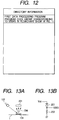
- Figs. 13A and 13B of the accompanying drawings illustrate the construction of a color measuring apparatus which can be utilized in a color image forming apparatus of this kind.
- Fig. 13A shows an example of the image detection thereof
- Fig. 13B shows an example of an image detection circuit (a circuit for converting the output current of a photodiode into a voltage).
- This example is an example of a sensor using a photodiode to detect reflected light from a toner.
- the reference numeral 201 designates a photodiode (sensor), and the reference numeral 102 denotes an LED which is a light source and which illuminates a toner with a constant amount of light.
- the reference numeral 104 designates a toner patch which is an object of detection formed on a conveyed transferring material 1, and reflected light 206 from this toner patch 104 enters the photodiode 201, whereby a photocurrent is generated.
- the photocurrent is converted into a photoelectric conversion output (voltage signal) V203 by a resistor 202.
- This photoelectric conversion output V203 reflects the amount of reflected light on the surface of a toner at real time.
- a color measuring apparatus can be formed by a sensor using such a photodiode.
- the LED 102 three LEDs of e.g. Red (R), Green (G) and Blue (B) differing in light emission spectrum from one another are provided for respective colors, and the respective LEDs are caused to emit light independently of one another for the toner patch which is the object of measurement, and the output of the sensor corresponding to each LED is obtained, whereby there can be obtained the R, G and B components of reflected light from the toner patch, and chromaticity such as L*a*b* or XYZ in color space processing or the like can be calculated.
- R Red
- G Green
- B Blue
- Fig. 14 of the accompanying drawings is a block diagram showing the pixel construction of a line sensor of an accumulation type utilized in a conventional color image forming apparatus.
- the reference numeral 204 denotes a sensor array comprising pixels 207 to 220.
- the reference numeral 205 designates a reading-out circuit, and the reference numeral 206 denotes a reset circuit.
- the pixels 207 to 209 and 220 are pixels of which the surfaces are shielded from light.
- the pixels 210 to 219 are a row of pixels responding to light.
- the pixels 207 and 220 serve also as dummy pixels absorbing the unevenness of a sensor characteristic by their being located at the end portions.
- Fig. 15 of the accompanying drawings is a timing chart illustrating the operation timing of the line sensor of the accumulation type shown in Fig. 14 .
- a reset pulse 221 is applied to a port P1 to thereby reset the sensor 201, whereafter the reset is released and accumulation is started.
- the accumulation capacity (not shown) of the sensor 201 is charged with a photocurrent conforming to the amount of incident light.
- the bits shielded from light have their accumulation capacity charged with a dark current generated by the pixel portion.
- a forwarding pulse 222 is applied to a port P2, whereupon the output of the sensor 201 is collectively forward to the reading-out circuit 205, and is outputted as an output signal 224 from a port P4 for each pixel on the basis of a shift pulse 223 inputted by a shift register in the reading-out circuit 205 through a port P3.
- an output corresponding to the dark pixel 208 is defined as a dark time output and is substrated from the outputs of the subsequent effective pixels, whereby there is obtained a signal in which an error amount by the dark current of the sensor 201 has been corrected.
- the color measuring apparatus can also be formed by such a cumulative type sensor.
- R, G and B filters are provided on the surface of the sensor, and the toner patch which is the object of measurement is illuminated by a light source like a white LED having a spectrum over the entire visible light area, and the output of the sensor 201 corresponding to each filter is obtained, whereby the R, G and B components of reflected light from the toner patch are obtained, and chromaticity such as L*a*b* or XYZ in the above-mentioned color space processing can be calculated.
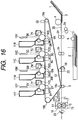
- Fig. 16 of the accompanying drawings is a. schematic cross-sectional view illustrating the construction of a color image forming apparatus of this kind, and corresponds, for example, to the case of a four-set tandem type color laser printer.
- the color laser printer forms an electrostatic latent image by image light formed on the basis of an image signal in an image forming portion, develops this electrostatic latent image to thereby form a visible image, further transfers this color visible image to a transferring material which is a recording medium, and then fixes the color visible image.
- the image forming portion is comprised of photosensitive drums 5Y, 5M, 5C, 5K, injection charging devices 7Y, 7M, 7C, 7K as primary charging means, developing devices 8Y, 8M, 8C, 8K and toner cartridges 11Y, 11M, 11C, 11K in respective stations juxtaposed by the number of developing colors, an intermediate transferring member 12, a sheet feeding portion, a transferring portion and a fixing portion 13.
- Each of the photosensitive drums 5Y, 5M, 5C and 5K is constituted by an aluminum cylinder and an organic photoconductive layer applied to the outer periphery thereof, and is rotated by the driving force of a drive motor, not shown, being transmitted thereto, and the drive motor counter-clockwisely rotates the photosensitive drums 5Y, 5M, 5C and 5K in conformity with an image forming operation.
- Exposure lights to the photosensitive drums 5Y, 5M, 5C and 5K are sent from scanner portions 10Y, 10M, 10C and 10K, and are selectively applied to the surfaces of the photosensitive drums 5Y, 5M, 5C and 5K, whereby electrostatic latent images are successively formed thereon.
- the primary charging means provision is made of the four injection charging devices 7Y, 7M, 7C and 7K for charging the yellow (Y), magenta (M), cyan (C) and black (K) photosensitive drums in the respective stations, and the respective injection charging devices are provided with sleeves 7YS, 7MS, 7CS and 7KS.
- the four developing devices 8Y, 8M, 8C and 8K for effecting yellow (Y), magenta (M), cyan (C) and black (K) development in the respective stations are provided to visualize the above-mentioned electrostatic latent images, and the respective developing devices are provided with sleeves 8YS, 8MS, 8CS and 8KS.
- the respective developing devices are detachably mounted with respect to an apparatus main body.
- the intermediate transferring member 12 is an endless belt member passed over a drive roller 18a and driven rollers 18b, 18c, is in contact with the photosensitive drums 5Y, 5M, 5C and 5K, is clockwisely rotated during color image forming, and is sequentially subjected to transfer by the action of primary transferring rollers 6Y, 6M, 6C and 6K for the respective colors.
- Transferring materials 1 are contained in a sheet feeding cassette 2 or a sheet feeding tray 3 as sheet feeding means (sheet feeding port), and the transferring materials 1 are conveyed one by one along a conveying path 25 constituted by a sheet feeding roller 4 and conveying rollers 24 and arrive at registration rollers 23. This is detected by an ante-registration sensor 19.
- the conveyance of the transferring material is stopped for a predetermined time by the ante-registration sensor 19 in timed relationship with the arrival of the color visible images on the intermediate transferring material 12 at a transferring area.
- the transferring material 1 is fed from the registration rollers 23 to the transferring area, and a secondary transferring roller 9 comes into contact with the intermediate transferring member 12 and nips and conveys the transferring material to thereby superimpose and transfer the color visible images on the intermediate transferring member 12 onto the transferring material 1 at a time.
- the secondary transferring roller 9 is brought into contact with the intermediate transferring member 12 as indicated by solid line as long as the color visible images are superimposed and transferred onto the intermediate transferring member 12, but it is brought to a spaced-apart position indicated by dotted line after the termination of the printing process.
- the fixing portion 13 serves to fix the transferred color visible images while conveying the transferring material 1, and is provided with a fixing roller 14 for heating the transferring material 1 and a pressure roller 15 for bringing the transferring material 1 into pressure contact with the fixing roller 14, as shown in Figs. 13A and 13B .
- the fixing roller 14 and the pressure roller 15 are formed into a hollow shape, and contain heaters 16 and 17, respectively, therein. That is, the transferring member 1 bearing the color visible image thereon is conveyed by the fixing roller 14 and the pressure roller 15 and also have heat and pressure applied thereto, whereby the toners are fixed on the surface thereof.
- the transferring material 1 is discharged to a sheet discharging portion, not shown, by discharge rollers, not shown, thus completing the image forming operation.
- the discharge of the transferring material 1 from the fixing portion is detected by a fixed sheet discharge sensor 20.
- Cleaning means 21 stores therein waste toners after the color visible images of the four colors formed on the intermediate transferring member 12 have been transferred to the transferring material 1.
- Color misregister detecting means 22 forms a color misregister detection patch on the transferring material, detects the amounts of misregister among the colors in a main scanning direction and a subscanning direction, and applies feedback so as to finely adjust image data to thereby reduce color misregister.
- process conditions such as several kinds of exposure amounts and developing biases corresponding to absolute humidity and gradation correcting means such as a look-up table (LUT) are provided for the toner of each color, and on the basis of the absolute humidity measured by a temperature and humidity sensor, not shown, the then process conditions and gradation correction value are selected.
- LUT look-up table
- a toner image for density detection (hereinafter referred to as the toner patch) is formed on the intermediate transferring member by a toner of each color, and this toner patch is detected by an optical sensor disposed at a location equivalent to the detecting means 22, and from the result thereof, feedback is applied to the process conditions such as the exposure amount and the developing bias and density control is effected to thereby obtain a stable image.
- the reflectance of the toner patch is various from a high level to a low level, and the output of the sensor 201 fluctuates from a nearly saturated output to nearly a dark-time output.
- the output thereof becomes small and is buried in the quantization error during the AD conversion of the signal or the noise of a reading-out system and a correct signal cannot be obtained.
- EP-A-1 310 832 discloses a color image forming apparatus and a method for controlling the same. This document essentially relates to density control and teaches control of a density sensor located prior to a fixing unit on the basis of a detection of a color sensor located after the fixing unit.
- the document WO-A-01/16567 discloses a system and a method for accurately reproducing color. This document essentially relates to color measurement on the basis of reflected light by distinguishing reflections from the surface of a patch image and reflections from the underlying substrate.
- the document WO-A-00/28289 discloses a method and a device for the colorimetric measurement of a colored surface. This document essentially relates to color measurement on the basis of an image-taking approach which is not based on reflected light.
- the present invention has been made in order to solve the above-noted problems and an object thereof is to provide a color image forming apparatus and a color measurement controlling method, which are capable of solving the above-noted problems.
- the present invention provides a color image forming apparatus and a color measurement controlling method, as defined in the appended claims.
- the color image forming apparatus and the color measurement controlling method according to the present invention can change a color measuring condition in adaptation to a reflectance predicted from the forming condition of color images to be detected and detect an amount of reflected light, adjust the image forming condition from the amount of reflected light of each of the detected color images to thereby accurately effect the color measurement of each color image irrespective of the reflectance of each color image, and accurately detect the hues and density of the color images which are the objects of detection and form a color image excellent in color reproducibility.
- the present invention encompasses a storage medium and a program capable of being read by a computer.
- Fig. 1 is a schematic cross-sectional view illustrating the construction of a color image forming apparatus according to a first embodiment of the present invention, and in Fig. 1 , the same members as those in Fig. 16 are given the same reference characters.
- the reference numeral 26 designates a color measuring apparatus which color-measures a patch image formed on a recording medium, at a position underlying the disposed position of a fixing portion B.
- the color measuring apparatus 26 is designed to be capable of being to changing a color measuring condition in adaptation to a reflectance predicted from the forming condition of a color image which is an object of detection, in accordance with a control procedure shown, for example, in Fig.
- the color measuring apparatus 26 is used as a sensor for detecting the colors of toners on paper after fixing and therefore is disposed at a location intermediate between the fixing portion 13 of Fig. 1 and a sheet discharging port (not shown).
- control can be effected so as to apply feedback to a process condition such as a developing bias and gradation correcting means such as a look-up table from the output of each of R, G and B sensors having read reflected light from a toner patch fixed on a transferring material 1 to thereby produce a desired hue on the transferring material.
- a process condition such as a developing bias and gradation correcting means such as a look-up table from the output of each of R, G and B sensors having read reflected light from a toner patch fixed on a transferring material 1 to thereby produce a desired hue on the transferring material.
- the reflectance of the toner patch is low, the amount of light of an LED can be increased to thereby take out an accurate signal without being buried in noise and therefore, the control of the image forming condition based on information of high accuracy becomes possible, and an improvement in the accuracy of color stabilization control can be achieved.
- the other operations of the image forming apparatus are the same as those of the example of the prior art and therefore need not be described.
- Fig. 2 is a circuit diagram showing an example of the detection circuit of the color measuring apparatus 26 shown in Fig. 1 .
- a light receiving portion is comprised of photodiodes 101R, 101G and 101B provided with R, G and B color filters, respectively.
- Photocurrents generated by the photodiodes 101R, 101G and 101B are converted into voltage signals by resistors 102R, 102G and 102B, and become output signals 111R, 111G and 111B impedance-converted by buffers 106, 107 and 108 comprised of operational amplifiers.
- an illuminating system is comprised of a white LED 103 having a light emission spectrum in an entire visible light area, and a driving current control circuit for the LED comprising an operational amplifier 105, a resistor 104 and an NPN transistor 110.
- a voltage signal 109 for controlling an electric current flowing to the white LED 103 is supplied from a DA converter, not shown.
- Feedback is applied to the operational amplifier 105 so that the voltage signal 109 inputted to the non-reversal input terminal of the operational amplifier 105 may be generated on the anode side of the resistor 104. Accordingly, an electric current determined by the voltage signal 109 and the resistance value of the resistor 104 flows to the emitter of the NPN transistor 110, and substantially the same collector current becomes a driving current for the white LED 103. Accordingly, by controlling the voltage level of the voltage signal 109, the driving current for the white LED 103 can be adjusted to thereby adjust the amount of emitted light.
- Fig. 3 illustrates the color measuring operation of the color measuring apparatus 26 shown in Fig. 1 .
- the reference numeral 112 designates the illuminating system
- the reference numeral 113 denotes the light receiving portion comprised of the three photodiodes.
- a patch of a single color C, M, Y or K or mixed colors of these is formed from the heads of the directions of arrows in Fig. 3 .
- the transferring material 1 to which respective developers are transferred is conveyed in the direction of arrow (leftwardly) in Fig. 3 , and toner patches 114 to 117 are formed on the transferring material 1.
- the reflectance of the toner patch 114 on the transferring material 1 is greatest, and the reflectance becomes gradually smaller and the reflectance of the toner patch 117 becomes smallest.
- Figs. 4A and 4B are characteristic graphs illustrating the detecting operation of the color measuring apparatus shown in Fig. 1 .
- Fig. 4A shows a predicted reflectance (foreseen reflectance) detected when the patches 114 to 117 shown in Fig. 3 are irradiated with a constant amount of light, along the directions of the axis of abscissas and the axis of ordinates of Fig. 4A.
- Fig. 4B shows the adjusted state of the amount of light of Fig. 4A to the patches 114 to 117, and the axis of ordinates of Fig. 4B indicates the amount of irradiating light, and the direction of the axis of abscissas indicates the respective patches 114 to 117.
- the light receiving portion 113 receives reflected lights from the toner patches 114 to 117 one after another, and outputs R, G and B signals 111R, 111G and 111B corresponding thereto.
- an input voltage applied to the illuminating system 112 can be changed in conformity with predicted reflectance to thereby adjust an LED driving current, i.e., the amount of light, and control so that the output may be substantially constant.
- the output 111 becomes small for a patch of low reflectance like the toner patch 117 corresponding to black, and the signal is buried in a quantization error when AD conversion is done or the noise of a reading-out circuit, and the R, G and B components of correct reflected light cannot be obtained.
- the sensor output is saturated with the patch 114 of e.g. Y color which is high in reflectance, and again in this case, correct color measurement becomes impossible.
- the R, G and B signals after AD-converted are converted into the values of the same amount of light condition (as an example, the amount of light of the LED is substantially proportional to the driving current and therefore can be multiplied by a value corresponding to the inverse number of the value of a DA converter set during measurement), and the chromaticity of the corresponding toner patch is calculated, and the image forming condition is changed so as to correct the deviation from desired chromaticity.
- the amount of light may be continuously changed in inverse proportion to the predicted reflectance (within such a range as will not exceed the upper limit of the allowable amount of light of the LED), or as shown in Fig. 5B , such stepwise control that a constant amount of light is set within a certain range of reflectance and if the range is exceeded, a new amount of light is set may be done.
- the sensor is not restricted to the photodiode, but of course may be a sensor like a phototransistor which generates an output current conforming to an incident light, or an accumulation type sensor like a CCD or a CMOS sensor which accumulates a photocurrent therein for a predetermined time, and thereafter converts it into a voltage and outputs it.
- each of the R, G and B components is varied by the hue of the patch and therefore, there is a patch of a hue which is great in the reflectance of the entire visible light but is small in the reflectances corresponding to the spectrum of the individual light sources.
- electric currents flowing to a plurality of light sources are changed for a toner patch to thereby control the output so as to be substantially constant.
- the amount of light of the light source is changed in conformity with the predicted reflectance of the toner patch by a circuit which will be described later, whereby the output is not saturated even for a toner patch of great reflectance (e.g. the Y patch), and the influence of the quantization error or the noise of the reading-out circuit during AD conversion can be reduced even for a patch of small reflectance (e.g. the K patch) and chromaticity information of high accuracy can be obtained.
- a toner patch of great reflectance e.g. the Y patch
- the influence of the quantization error or the noise of the reading-out circuit during AD conversion can be reduced even for a patch of small reflectance (e.g. the K patch) and chromaticity information of high accuracy can be obtained.
- a sensor of the accumulation type typified, for example, by a CMOS sensor is used as the light receiving portion 113 of the color measuring apparatus shown in Fig. 3 .
- the white LED 103 of the illuminating system use is made of a white LED having a spectrum in the entire visible light area as in the first embodiment and therefore, this need not be described.
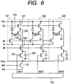
- Fig. 6 illustrates the construction of a circuit in the color measuring apparatus of a color image forming apparatus according to a second embodiment of the present invention, and in the present embodiment, an accumulation type sensor of a CMOS type is used as a sensor element.
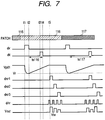
- Fig. 7 is a timing chart illustrating the operation of the CMOS sensor shown in Fig. 6 . Description will hereinafter be made of the operation of a pixel of the CMOS sensor.
- the reference numeral 124 designates a photodiode for detecting light.
- the reference numeral 125 denotes NMOSFET for resetting the photodiode to reset potential Vr on the basis of a sensor reset signal ⁇ r
- the reference numeral 126 designates PMOSFET for outputting the anode potential Vpd of the photodiode 124 by a source follower.
- the reference numeral 127 denotes PMOSFET to the gate of which a constant voltage Vb is applied and which supplies a constant current to the source follower:
- the reference numeral 128 designates NMOSFET for collectively forwarding the outputs of respective sensors to a capacitor 129 on the basis of a forwarding signal ⁇ t.
- the reference numeral 130 denotes NMOSFET for outputting the charges forwarded to the capacitor 129 to an output line Vout in conformity with the output ⁇ sr1 of a shift register 132.
- the reference numeral 131 designates NMOSFET for resetting the output line Vout to a voltage Vhr on the basis of an output line reset signal ⁇ hr.
- the senor shown in Fig. 6 is provided for three pixels (pixels 121, 122, 123) correspondingly to R, G and B colors, and R, G and B on-chip color filters are provided on the surfaces of the respective pixels, whereby it becomes possible to detect signals of three colors, i.e., R, G and B, of reflected light.
- the signal outputted to the output line Vout is buffered by an operational amplifier or the like, and thereafter is AD-converted, whereby it is possible to obtain a signal resulting from lights corresponding to the wavelengths of R, G and B components of reflected light reflected by the surface of the toner having been accumulated for a predetermined time.
- Each driving signal is supplied from a CPU or the like (not shown) for controlling the operation of the color image forming apparatus.
- CMOS sensor in the present embodiment will hereinafter be described with reference to the timing chart of Fig. 7 .
- patches to be detected are formed on the transferring material 1 in each image station on the basis of stored patch image data.
- the white LED 103 of the illuminating system shown in Fig. 3 is continuously made to emit light by a constant electric current throughout detection.
- the sensor reset signal ⁇ r assumes a high state (H) at a timing time t1, and the NMOSFET 125 is turned on and the anode of the photodiode is reset to the voltage Vr.
- the sensor reset signal ⁇ r assumes a low state (L), and when the reset of the photodiode 124 is released, the accumulation by the sensor is started.
- the timing of the timing time t2 is set to a state in which the toner patch on the transferring material has sufficiently entered the detection range of the sensor, in order to avoid the color mixing with the adjacent toner patch during color measurement.
- the anode potential Vpd1 of the photodiode 124 rises by the photocurrent by the R component of the incident light.
- the anode potentials Vpd2 and Vpd3 of the photodiodes of pixels 122 and 123 rise in conformity with the intensity of the G component and B component of the incident light.
- the forwarding signal ⁇ t is brought into a high state (H), whereupon the NMOSFET 128 is turned on, and an output voltage resulting from the anode potential Vpd1 having been buffered by a source follower circuit is forwarded to the capacitor 129.
- the forwarding signal ⁇ t assumes a low state (L), thereby terminating the forwarding to the capacitor 129.
- This interval becomes an accumulation time (ts) 116.
- the pixels 122 and 123 likewise operate.
- the shift register 132 is operated to thereby bring a shift pulse ⁇ sr1 into a high state (H) and the NMOSFET 130 is turned on to thereby read out an output pulse Vout which is the output of the sensor.
- the output pulse Vout thus read out is AD-converted by an AD converter (not shown) and is contained in the memory of a CPU (not shown) which controls the operation of the image forming apparatus.
- the output line brings the pulse ⁇ hr into a high state (H), whereby it is reset to a reset pulse Vhr by the NMOSFET 131.
- the shift register turns on shift pulses ⁇ sr2 and ⁇ sr3 one after another and reads out sensor outputs corresponding to the subsequent G and B filters.
- the detection of the toner patch 117 is likewise effected.
- the accumulation time (ts117) in this case is increased or decreased in conformity with the reflectance predicted from the image forming condition.
- the density of the toner patch 117 is high and the reflectance predicted from the image forming condition is low and therefore, the accumulation time ts117 corresponding to the toner patch 117 is made longer than ts116, and with respect also to the patch of low reflectance, the output of the sensor is made great as compared with the quantization error during AD conversion or the noise level of the reading-out system.
- the accumulation time is made short to thereby prevent the saturation of the sensor.
- R, G and B signals corresponding to a plurality of toner patches after AD-converted are converted into the values under the condition of the same accumulation time (as an example, they may be multiplied by a value corresponding to the inverse number of the accumulation type during measurement), and the chromaticity of the corresponding toner patch is calculated, and feedback is applied to several kinds of exposure amounts conforming to the absolute humidity corresponding to the toner of each color, the process condition such as the developing bias, and the gradation correcting means such as the look-up table to thereby control so as to provide a desired hue on the transferring material, but this is similar to the case of the first embodiment and therefore need not be described.
- Figs. 8A and 8B are characteristic graphs illustrating the correspondence of the accumulation time and the predicted reflectance to the capacitor 129 shown in Fig. 6 .
- Fig. 8A corresponds to a case where the accumulation time is continuously changed so as to be inversely proportional to the predicted reflectance
- Figs. 8A and 8B show an example in which in the case of a reflectance within a certain range.
- the accumulation time is stepwisely changed so as to be constant.
- the axis of ordinates indicates the accumulation time and the axis of abscissas indicates the predicted reflectance.
- the relation between the predicted reflectance of the toner patches and the accumulation time is such that it is basic to make the accumulation time long for the toner patch of smaller reflectance, but as shown in Fig. 8A .
- the accumulation time may be continuously changed so as to be inversely proportional to the predicted reflectance, or as shown in Fig. 8B , in the case of a reflectance within a certain range, the accumulation time may be stepwisely changed so as to be constant.
- the accumulation type sensor is used and the accumulation time thereof is changed in conformity with the reflectance predicted from the image forming condition of the toner patches, whereby without the adjustment of the amount of light of the LED for each toner patch, the influence of the quantization error during AD conversion or the noise of the reading-out circuit can be reduced even for the toner patch of small reflectance, and color information of high accuracy can be obtained. Further, an improvement in the color stability of the color image forming apparatus can be realized by the use of the obtained information.
- the example of three sensors carrying three R, G and B filters thereon has been shown as the sensor for detecting the chromaticity of the toners.
- the number of the sensors is not limited to three, but of course, in order to make symmetry good, a plurality of dummy pixels may be provided on both sides, or a plurality of pixels corresponding to R, G and B filters may be provided, and such control as takes the sum or average of the outputs thereof and averages the positional unevenness of the toner patches to thereby improve accuracy may be effected.
- the wavelengths transmitted through the filters are not limited to R, G and B.
- the example of the CMOS sensor has been shown as the accumulation type sensor.
- the kind of the sensor is not particularly restricted, but use may be made of any accumulation type sensor such as CCD or BASIS.
- the present embodiment is characterized in that design is made such that not only the accumulation time of the accumulation type sensor is changed in conformity with the reflectance predicted from the forming condition of the toner patches, but the lengths of the toner patches in the conveyance direction are made variable.
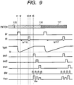
- Fig. 9 is a timing chart illustrating the operation of the CMOS sensor shown in Fig. 6 , and in Fig. 9 , the same reference characters as those in Fig. 7 are the same in significance. This example of the operation will also be described with respect to the patches 116 and 117 of the toners of relatively low reflectance as in the second embodiment.
- toner patches having their lengths changed in conformity with the reflectance predicted from the forming condition of the respective patches are formed on the transferring material 1.
- the white LED 103 of the illuminating system shown in Fig. 3 is continuously made to emit light by a constant electric current throughout patch detection.
- the reset signal ⁇ r assumes a high state (H), the NMOSFET 125 is turned on and the anode of the photodiode is reset to a voltage Vr.
- the reset signal ⁇ r assumes a low state (L), and when the reset of the photodiode 124 is released, accumulation is started.
- the potential Vpd1 of the anode of the photodiode 124 rises by a photocurrent.
- the potentials Vpd2 and Vpd3 of the anodes of the photodiodes of the pixels 122 and 123 rise in conformity with the intensity of the incident light.
- ⁇ t is brought into a low state (L), thus terminating the forwarding to the capacitor 129.
- This time is an accumulation time t2 116.
- the shift register 132 is operated, and at the timing time t5, ⁇ sr1 is brought into a high state (H), the NMOSFET 130 is turned on, and the output of the sensor is read out at Vout.
- the signal thus read out is AD-converted by an AD converter (not shown) and is contained in the memory of a CPU (not shown) for controlling the operation of the image forming apparatus.
- the output line brings ⁇ hr into a high state (H), whereby it is reset to Vhr by the NMOSFET 121.
- the shift register turns on ⁇ sr2 and ⁇ sr3 one after another, and reads out sensor outputs corresponding to the subsequent G and B color filters.
- the detection of the toner patch 117 is likewise effected.
- the density of the toner patch 117 is high and the reflectance predicted from the image forming condition is low and therefore, the accumulation time ts117 corresponding to the toner patch 117 is made longer than ts116, and with respect also to the patches of low reflectance, the output of the sensor is made great as compared with the quantization error during AD conversion or the noise level of the reading-out system, as in the second embodiment.
- the lengths of the patches along the conveyance direction are changed in conformity with the predicted reflectance.
- the length of the toner patch 117 of relatively low reflectance along the conveyance direction is lengthened and therefore, even if the accumulation time is lengthened, the detection range of the sensor does not extend to the next patch and detection can be effected.
- the length of the patch along the conveyance direction and the accumulation time can be made short, and the limited length of the transferring material can be efficiently used and color measurement of high accuracy becomes possible without the number of detectable patches being decreased.
- R, G and B signals corresponding to a plurality of toner patches after AD-converted are converted into the value of the condition of the same accumulation time (as an example, they can be multiplied by a value corresponding to the inverse number of the accumulation time during measurement), the chromaticity of the corresponding toner patch is calculated, and feedback is applied to the process condition such as the developing bias and the gradation correcting means such as a look-up table so as to provide a desired hue on the transferring material, but this is similar to the case of the first embodiment and therefore need not be described.
- the relation between the predicted reflectance of the toner patch and the accumulation time is such that it is basic to make the accumulation time longer for the patch of smaller reflectance, but as shown in Fig. 8A , the accumulation time may be continuously changed so as to be inversely proportional to the predicted reflectance, or as shown in Fig. 8B , in the case of a certain range of reflectance, the accumulation time may be changed so as to be made constant.
- the length of the patch in the conveyance direction conforming to the predicted reflectance of the toner patch, it is basic to make the patch of smaller reflectance longer, but as shown in Fig. 10A , the length of the patch may be continuously changed so as to be inversely proportional to the predicted reflectance, or as shown in Fig. 10B , in the case of a certain range of reflectance, the length of the patch may be stepwisely changed so as to be made constant.
- the accumulation type sensor is used and the accumulation time thereof is changed in conformity with the reflectance predicted from the image forming condition of the toner patch, whereby without the adjustment of the amount of light of the LED for each toner patch, the influence of the quantization error during AD conversion or the noise of the reading-out circuit can be reduced even for a toner patch of small reflectance, and color information of high accuracy can be obtained.
- the length of the patch can be changed in conformity with the predicted reflectance thereof, whereby the limited length of the transferring material can be effectively used to thereby realize the color measurement of high accuracy, and by the use of information obtained therefrom, an improvement in the color stability of the color image forming apparatus can be realized.
- the example of three sensors having three R, G and B filters put thereon has been shown as the sensor for detecting the chromaticity of the toner.
- the number of sensors is not restricted to three, but in order to make symmetry good, of course, such control as provides a plurality of dummy pixels on both sides or provides a plurality of pixels corresponding to the R, G and B filters, and takes the sum or average of the outputs thereof and averages the positional unevenness of the toner patches to thereby improve accuracy may be effected.
- the wavelengths transmitted through the filters are not limited to R, G and B.
- CMOS sensor has been shown as the accumulation type sensor.
- the kind of the sensor is not particularly restrictive, but use may be made of any accumulation type sensor such as CCD or BASIS.
- reflectance is predicted from the forming condition of the toner patch, and the amount of light and the accumulation time are controlled.
- This method is premised on that image forming is effected normally, and when the image forming condition remarkably deviates from a normal state, there is the possibility that the sensor output is saturated (when the reflectance deviates toward an extremely great side) or conversely the signal level becomes extremely small.
- design may be made such that the color measuring apparatus controls the amount of light and the accumulation time on the basis of not only the reflectance predicted from the forming condition of the toner patch but also the actually measured reflectance by the CPU executing a measurement control program stored in a ROM provided on a controller substrate, not shown, so that accurate color measurement may be made possible even when the image forming condition remarkably deviates from the normal state.
- This embodiment will hereinafter be described.
- the construction of the image forming apparatus corresponds to that of the color image forming apparatus shown in Fig. 1 .
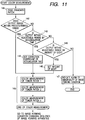
- Fig. 11 is a flow chart showing an example of the color measuring process procedure in the color image forming apparatus according to the present invention. Numbers (141) to (148) designate steps.
- the color measurement of a standard patch of a mixture of C, M, Y and K (141), and the magnitudes of the signal levels are judged (142), and if it is judged that the signal levels of the sensors of the color measuring apparatus are normal, the detection of the toner patches is effected by the method shown in the color measuring process of one of the first embodiment to the third embodiment (148).
- step (142) it is judged that the signal levels of the sensors of the color measuring apparatus are not normal, at a step 143, whether the signal levels are not normal, but yet are not extremely great or small and are correctable by the adjustment of the accumulation time is judged, and if it is judged that they are correctable by the adjustment of the accumulation time, at a step (144), an accumulation time correction coefficient is set, and advance is made to a step (148).
- the accumulation time correction coefficient is a coefficient to multiply the accumulation times of all toner patches when the accumulation time adjustment as shown in the second embodiment and the third embodiment is effected to thereby detect the reflected light from the toner patches, and a case where there is particularly no abnormality in the image forming condition, but a predetermined signal level is obtained is "1", and a case where the signal level is too small is a coefficient greater than "1".
- the upper limit is such a value that in case of color measurement, the detection area of the sensor does not extend to the next patch.
- the upper limit is a value smaller than "1".
- step (143) it is judged that the signal level is not correctable by the adjustment of the accumulation time
- step (145) that is, if the signal level of the standard patch is outside the range correctable by the adjustment of the accumulation time, whether the signal level is within a range adjustable by the amount of light is judged.
- the maximum amount of light is determined by the rated current of the LED and therefore, the range adjustable by the amount of light is limited.
- a new amount of light is set (146), and advance is made to the step (148).
- the step (145) if at the step (145), it is judged that the signal level is not within the range adjustable by the amount of light, that is, the signal level is outside such range, at a step (147), the alarm of the abnormality of the image forming condition is put out, thus ending the patch detecting process.
- the toner patches 1-n are color-measured, thus ending the measurement.
- the accumulation time or the amount of light of the light source is adjusted on the basis of the magnitude (the reflectance of the patch) of the signal actually read from the patch, whereby the accurate color measurement of the patch becomes possible.
- Fig. 12 shows the memory map of a storage medium such as a floppy disc or a CD-ROM storing therein various data processing programs readable out by the color image forming apparatus according to the present invention.
- information for controlling a program group stored in the storage medium for example, version information, the name of a program maker, etc. is also stored, and information depending on the OS or the like of the program reading side, for example, icon or the like for discriminating and indicating the program is also stored.
- data belong-ing to the various programs are controlled by the above-described directory.
- a program for installing the various programs in a computer, and a program or the like for thawing the program for installing when it is compressed are also stored.
- the function in the present embodiment shown in Fig. 11 may be performed by a host computer by the use of a program installed from the outside.
- the present invention is also applied when an information group including the program is supplied to an output apparatus by a storage medium such as a CD-ROM, a flash memory or an FD, or from an external storage medium through a network.
- the object of the present invention is also achieved by supplying a system or an apparatus with the storage medium having recorded therein the program code of software for realizing the function of the aforedescribed embodiments, as described above, and the computer (or the CPU or MPU) of the system or the apparatus reading out and executing the program code stored in the storage medium.
- the program code itself read out of the storage medium realizes the novel function of the present invention and thus, the storage medium storing the program code therein constitutes the present invention.
- the storage medium for supplying the program code use can be made, for example, of a flexible disc, a hard disc, an optical disc, a magneto-optical disc, a CD-ROM, a CD-R, a magnetic tape, a nonvolatile memory card, a ROM, an EEPROM or the like.
- the present- invention also covers a case where a program code read out by a computer is executed, whereby not only the function of the aforedescribed embodiments is realized, but also on the basis of the instructions of the program code, an operating system (OS) or the like working on the computer carries out part or the whole of actual processing, and the function of the aforedescribed embodiments is realized by that processing.
- OS operating system
- the present invention also covers a case where the program code read out of the storage medium is written into a memory provided in a function expanding board inserted into a computer or a function expanding unit connected to the computer, whereafter on the basis of the instructions of the program code, a CPU or the like provided in the function expanding board or the function expanding unit carries out part or the whole of actual processing, and the function of the aforedescribed embodiments is realized by that processing.
- the amount of light of the light source of the color measuring apparatus is controlled in conformity with the reflectance predicted from the forming condition of the toner patch and specifically, in a color measuring apparatus for detecting the reflected light from the toner patch on the transferring material to thereby find chromaticity, the amount of light of the light source is changed in conformity with the reflectance of the toner patch, and even for a patch of small reflectance, the signal components are made great and then read and therefore, the influence of the quantization error during AD conversion or the noise of the reading-out circuit can be reduced, and irrespective of the reflectance of the patch, color measurement of high accuracy becomes possible.
- the present color measuring apparatus is carried on the color image forming apparatus, and the chromaticity obtained from the toner patch is fed back to the image forming condition, whereby an image of a stable hue can be obtained.
- the amount of light of the light source is controlled, whereby even toner patch of low reflectance can be read out at a great signal level and detection good in S/N and reduced in the influence of the quantization error or the noise of the circuit can be accomplished.
- the accumulation time of the accumulation type sensor of the color measuring apparatus is controlled in conformity with the reflectance predicted from the forming condition of the toner patch and specifically, in a color measuring apparatus for detecting the reflected light form the toner patch on the transferring material to thereby find chromaticity, the accumulation time of the accumulation type sensor is changed in conformity with the reflectance of the toner patch, and even for a patch of small reflectance, the signal components are made great and then read and therefore, the influence of the quantization error during AD conversion or the noise of the reading-out circuit can be reduced, and irrespective of the reflectance of the patch, color measurement of high accuracy becomes possible.
- the amount of light of the light source is not changed and therefore, when the amount of light is to be changed, it is unnecessary to wait for color measurement until the amount of light becomes stable, and it is possible to increase the number of detectable patches for the limited length of the transferring material.
- controlling the accumulation time enables even a toner patch of low reflectance to be read at a great signal level, and enables detection good in S/N and reduced in the influence of the quantization error or the noise of the circuit to be accomplished.
- the present color measuring apparatus when the present color measuring apparatus is carried on the color image forming apparatus and the chromaticity obtained from the toner patch is to be fed back to the image forming condition, feedback can be applied on the basis of the information from more patches, and an image of a more stable hue can be obtained.
- the accumulation time of the accumulation type sensor of the color measuring apparatus and the length of the toner patch in the conveyance direction are controlled in conformity with the reflectance predicted from the forming condition of the toner patch, and specifically in a color measuring apparatus for detecting the reflected light from the toner patch on the transferring material to thereby find chromaticity, when the accumulation time of the accumulation type sensor is changed in conformity with the reflectance of the toner patch, the length of the toner patch is also changed, namely, is controlled, in conformity with the reflectance, to thereby prevent the color mixing with the adjacent toner patch when color measurement is effected with the accumulation time extended, and also the length of the transferring material can be effectively utilized to accurately detect as many toner patches as possible within the limited length of the transferring material.
- the amount of light of the light source of the color measuring apparatus and the accumulation time of the accumulation type sensor are controlled in conformity with the reflectance predicted from the forming condition of the toner patch and the actually measured reflectance (signal level) of the patch and therefore, changing the color measuring condition in conformity with the actually measured reflectance of the patch enables the toner patch to be accurately color-measured even if the image forming condition deviates form the normal state.
- color measurement is effected with the measuring condition changed depending on not only the forming condition of the toner patch, but also the actually measured intensity of the reflected light from the patch and therefore, even if the image forming condition of the toner patch deviates from the normal state, irrespective of the reflectance of the toner patch, there is obtained a sufficient signal amplitude difficult to be affected by the quantization error or the noise of the reading-out circuit and thus, color measurement of good accuracy becomes possible.
- the amount of reflected light is detected with the color measuring condition changed in adaptation to the reflectance predicted from the forming condition of color images to be detected, and the image forming condition is adjusted from the amount of reflected light of each of the detected color images and therefore, irrespective of the reflectance of each color image, the color measurement of each color image is accurately effected to thereby accurately detect the hues and density of the color images to be detected, and a color image excellent in color reproducibility can be formed.
- a color image forming apparatus when a white LED is made to emit light to thereby detect reflected light from a color image, changes a color measuring condition in adaptation to a reflectance predicted from the forming condition of the color image to be detected and detects the amount of reflected light by photodiodes (R,G,B), and adjusts the image forming condition from the detected amount of reflected light of each color image.
- the color measurement of each color image is effected with good accuracy, and the hue and density of the color image to be detected are accurately detected to thereby form a color image excellent in color reproducibility.
Landscapes
- Physics & Mathematics (AREA)
- Spectroscopy & Molecular Physics (AREA)
- General Physics & Mathematics (AREA)
- Engineering & Computer Science (AREA)
- Life Sciences & Earth Sciences (AREA)
- Mathematical Physics (AREA)
- Theoretical Computer Science (AREA)
- Health & Medical Sciences (AREA)
- Microelectronics & Electronic Packaging (AREA)
- Chemical & Material Sciences (AREA)
- Analytical Chemistry (AREA)
- Biochemistry (AREA)
- General Health & Medical Sciences (AREA)
- Immunology (AREA)
- Pathology (AREA)
- Color Electrophotography (AREA)
- Control Or Security For Electrophotography (AREA)
Claims (18)
- Farbbilderzeugungsvorrichtung, die konfiguriert ist zum Anwenden einer Rückkopplung auf eine Bilderzeugungsbedingung eines Ausgabebilds basierend auf einem vorhergesagten Reflexionsgrad eines Detektionsbilds, mit:einer Farbbilderzeugungseinrichtung (5, 6, 7, 8, 10, 11) zum Erzeugen von Bildern jeweiliger Entwicklerfarben auf einem Übertragungsmaterial gemäß einer Bilderzeugungsbedingung;einer Farbmesseinrichtung (26), angeordnet an einer Stelle nach einer Fixiereinrichtung zum Fixieren der auf dem Übertragungsmaterial erzeugten Bilder, zum Anwenden von Licht auf Bilder jeweiliger Entwicklerfarben, die auf dem Übertragungsmaterial erzeugt sind, und Detektieren von reflektiertem Licht von den Bildern durch einen optischen Sensor,gekennzeichnet durch:eine Vorhersageeinrichtung zum Vorhersagen eines vorhergesagten Reflexionsgrads von Licht, das von als Detektionsbilder dienenden Bildern reflektiert wird, aus der Bilderzeugungsbedingung dieser Detektionsbilder,eine Einstelleinrichtung zum variablen Einstellen einer Detektionsbedingung der Farbmesseinrichtung im Einklang mit dem vorhergesagten Reflexionsgrad der Detektionsbilder, sodass das Ausgabesignal des optischen Sensors nicht in Rauschen begraben und nicht gesättigt ist; undeine Steuereinrichtung zum Anpassen der Bilderzeugungsbedingung von als Ausgabebilder dienenden Bildern, welche eine Prozessbedingung zum Hervorbringen eines gewünschten Farbtons der Ausgabebilder ist, auf Grundlage des reflektierten Lichts, das durch die Farbmesseinrichtung gemäß der durch die Einstelleinrichtung eingestellten Detektionsbedingung detektiert wird,wobei die Detektionsbedingung eine Lichtmenge einer Lichtquelle ist oder die Detektionsbedingung eine Ansammlungszeit eines Ansammlungstypsensors ist oder die Detektionsbedingung eine Ansammlungszeit eines Ansammlungstypsensors und eine Länge der detektierten Bilder entlang einer Beförderungsrichtung ist.
- Farbbilderzeugungsvorrichtung gemäß Anspruch 1, wobei, wenn die Detektionsbedingung eine Lichtmenge einer Lichtquelle ist, die Lichtmenge der Lichtquelle als die Detektionsbedingung änderbar ist, um verringert zu werden, wenn der vorhergesagte Reflexionsgrad größer ist, und um erhöht zu werden, wenn der vorhergesagte Reflexionsgrad kleiner ist.
- Farbbilderzeugungsvorrichtung gemäß Anspruch 1, wobei, wenn die Detektionsbedingung eine Ansammlungszeit eines Ansammlungstypsensors ist, die Ansammlungszeit als die Detektionsbedingung änderbar ist, um verringert zu werden, wenn der vorhergesagte Reflexionsgrad größer ist, und um erhöht zu werden, wenn der vorhergesagte Reflexionsgrad kleiner ist.
- Farbbilderzeugungsvorrichtung gemäß Anspruch 1, wobei, wenn die Detektionsbedingung eine Ansammlungszeit eines Ansammlungstypsensors und eine Länge der detektierten Bilder entlang einer Beförderungsrichtung ist, die Länge der detektierten Bilder entlang der Beförderungsrichtung als die Detektionsbedingung verkürzt wird, wenn der vorhergesagte Reflexionsgrad größer ist, und verlängert wird, wenn der vorhergesagte Reflexionsgrad kleiner ist.
- Farbbilderzeugungsvorrichtung gemäß Anspruch 1, wobei die Farbmesseinrichtung versehen ist mit einer Lichtquelle (112) mit einem Spektrum über ein gesamtes sichtbares Licht und einem Sensor (113) mit Pixeln, die mit drei oder mehr Filtern mit einer Spektralcharakteristik versehen sind.
- Farbbilderzeugungsvorrichtung gemäß Anspruch 1, wobei die Farbmesseinrichtung versehen ist mit drei oder mehr Lichtquellen mit unterschiedlichen Spektren und ein oder mehr Sensoren.
- Farbbilderzeugungsvorrichtung gemäß Anspruch 1, wobei die Farbmesseinrichtung versehen ist mit einer Lichtquelle mit einem Spektrum über ein gesamtes sichtbares Licht und einem Sensor mit einer Einrichtung zum Trennen des reflektierten Lichts von den Bildern und einer Vielzahl von Pixeln zum Messen der Stärke der getrennten Lichter.
- Farbbilderzeugungsvorrichtung gemäß Anspruch 1, wobei die Farbmesseinrichtung versehen ist mit drei oder mehr Lichtquellen mit unterschiedlichen Spektren und ein oder mehr Sensoren, und, wenn die Lichtquellen einen nach der anderen eingeschaltet werden und reflektierte Lichter, die den jeweiligen Lichtquellen entsprechen, durch den Sensor oder die Sensoren detektiert werden, die Lichtmenge von jeder Lichtquelle im Einklang mit einem vorhergesagten Spektralreflexionsgrad geändert wird.
- Farbbilderzeugungsvorrichtung gemäß Anspruch 1, wobei die Einstelleinrichtung, wenn sie die Detektionsbedingung einstellt, angepasst ist zum Bewirken der Einstellung der Detektionsbedingung im Einklang mit dem tatsächlich gemessenen Reflexionsgrad der Bilder, zusätzlich zu dem vorhergesagten Reflexionsgrad.
- Farbmessungssteuerverfahren für eine Farbbilderzeugungsvorrichtung, die konfiguriert ist zum Anwenden einer Rückkopplung auf eine Bilderzeugungsbedingung eines Ausgabebilds basierend auf einem vorhergesagten Reflexionsgrad eines Detektionsbilds, mit:einem Farbbilderzeugungsschritt des Erzeugens von Bildern jeweiliger Entwicklerfarben auf einem Übertragungsmaterial gemäß einer Bilderzeugungsbedingung;einem Farbmessschritt des Anwendens von Licht auf Bilder jeweiliger Entwicklerfarben, die auf dem Übertragungsmaterial erzeugt sind, und des Detektierens von reflektiertem Licht von den Bildern durch einen optischen Sensor nach einem Fixierschritt des Fixierens der auf dem Übertragungsmaterial erzeugten Bilder,gekennzeichnet durch:einen Vorhersageschritt des Vorhersagens eines vorhergesagten Reflexionsgrads von Licht, das von als Detektionsbilder dienenden Bildern reflektiert wird, aus der Bilderzeugungsbedingung dieser Detektionsbilder,einen Einstellschritt des variablen Einstellens einer Detektionsbedingung des Farbmessschritts im Einklang mit dem vorhergesagten Reflexionsgrad der Detektionsbilder, sodass das Ausgabesignal des optischen Sensors nicht in Rauschen begraben und nicht gesättigt ist; undeinen Steuerschritt des Anpassens der Bilderzeugungsbedingung von als Ausgabebilder dienenden Bildern, welche eine Prozessbedingung zum Hervorbringen eines gewünschten Farbtons der Ausgabebilder ist, auf Grundlage des reflektierten Lichts, das in dem Farbmessschritt gemäß der durch den Einstellschritt variabel eingestellten Detektionsbedingung detektiert wird,wobei die Detektionsbedingung eine Lichtmenge einer Lichtquelle ist oder die Detektionsbedingung eine Ansammlungszeit eines Ansammlungstypsensors ist oder die Detektionsbedingung eine Ansammlungszeit eines Ansammlungstypsensors und eine Länge der detektierten Bilder entlang einer Beförderungsrichtung ist.
- Farbmessungssteuerverfahren gemäß Anspruch 10, wobei, wenn die Detektionsbedingung eine Lichtmenge einer Lichtquelle ist, die Lichtmenge der Lichtquelle als die Detektionsbedingung verringert wird, wenn der vorhergesagte Reflexionsgrad größer ist, und erhöht wird, wenn der vorhergesagte Reflexionsgrad kleiner ist.
- Farbmessungssteuerverfahren gemäß Anspruch 10, wobei, wenn die Detektionsbedingung eine Ansammlungszeit eines Ansammlungstypsensors ist, die Ansammlungszeit als die Detektionsbedingung verringert wird, wenn der vorhergesagte Reflexionsgrad größer ist, und erhöht wird, wenn der vorhergesagte Reflexionsgrad kleiner ist.
- Farbmessungssteuerverfahren gemäß Anspruch 10, wobei, wenn die Detektionsbedingung eine Ansammlungszeit eines Ansammlungstypsensors und eine Länge der detektierten Bilder entlang einer Beförderungsrichtung ist, die Länge des Bilds entlang der Beförderungsrichtung als die Detektionsbedingung verkürzt wird, wenn der vorhergesagte Reflexionsgrad größer ist, und verlängert wird, wenn der vorhergesagte Reflexionsgrad kleiner ist.
- Farbmessungssteuerverfahren gemäß Anspruch 10, wobei der Farbmessschritt ausgeführt wird durch eine Lichtquelle mit einem Spektrum über ein gesamtes sichtbares Licht und einen Sensor mit Pixeln, die mit drei oder mehr Filtern mit einer Spektralcharakteristik versehen sind.
- Farbmessungssteuerverfahren gemäß Anspruch 10, wobei der Farbmessschritt ausgeführt wird durch drei oder mehr Lichtquellen mit unterschiedlichen Spektren und ein oder mehr Sensoren.
- Farbmessungssteuerverfahren gemäß Anspruch 10, wobei der Farbmessschritt ausgeführt wird durch eine Lichtquelle mit einem Spektrum über ein gesamtes sichtbares Licht und einen Sensor mit einer Einrichtung zum Trennen des reflektierten Lichts von den Bildern und einer Vielzahl von Pixeln zum Messen der Stärken der getrennten Lichter.
- Farbmessungssteuerverfahren gemäß Anspruch 10, wobei der Farbmessschritt ausgeführt wird durch drei oder mehr Lichtquellen mit unterschiedlichen Spektren und ein oder mehr Sensoren und einen Schritt des Einschaltens der Lichtquellen eine nach der anderen und des Änderns der Lichtmenge von jeder Lichtquelle im Einklang mit dem vorhergesagten Spektralreflexionsgrad umfasst, wenn die reflektierte Lichter, die den jeweiligen Lichtquellen entsprechen, durch den Sensor oder die Sensoren detektiert werden.
- Farbmessungssteuerverfahren gemäß Anspruch 10, wobei im Fall des Einstellens der Detektionsbedingung in dem Einstellschritt das Einstellen der Detektionsbedingung im Einklang mit den tatsächlich gemessenen Reflexionsgraden der Bilder, zusätzlich zu dem vorhergesagten Reflexionsgrad, bewirkt wird.
Applications Claiming Priority (2)
| Application Number | Priority Date | Filing Date | Title |
|---|---|---|---|
| JP2003033516A JP2004245931A (ja) | 2003-02-12 | 2003-02-12 | カラー画像形成装置およびカラー画像形成装置の測色制御方法およびコンピュータが読み取り可能な記憶媒体およびプログラム |
| JP2003033516 | 2003-02-12 |
Publications (3)
| Publication Number | Publication Date |
|---|---|
| EP1460480A2 EP1460480A2 (de) | 2004-09-22 |
| EP1460480A3 EP1460480A3 (de) | 2011-11-30 |
| EP1460480B1 true EP1460480B1 (de) | 2018-07-04 |
Family
ID=32820989
Family Applications (1)
| Application Number | Title | Priority Date | Filing Date |
|---|---|---|---|
| EP04003046.2A Expired - Lifetime EP1460480B1 (de) | 2003-02-12 | 2004-02-11 | Farbbilderzeugungsgerät und hierfür Steuerungsverfahren zur Farbmessung |
Country Status (4)
| Country | Link |
|---|---|
| US (1) | US7111784B2 (de) |
| EP (1) | EP1460480B1 (de) |
| JP (1) | JP2004245931A (de) |
| CN (1) | CN1521575B (de) |
Families Citing this family (16)
| Publication number | Priority date | Publication date | Assignee | Title |
|---|---|---|---|---|
| US20080054320A1 (en) * | 2006-08-31 | 2008-03-06 | Micron Technology, Inc. | Method, apparatus and system providing suppression of noise in a digital imager |
| JP4965961B2 (ja) * | 2006-10-12 | 2012-07-04 | キヤノン株式会社 | 画像形成装置 |
| KR20080080841A (ko) * | 2007-03-02 | 2008-09-05 | 주식회사 아이센스 | 전기화학적 바이오센서 및 이의 측정기 |
| US8687193B2 (en) * | 2008-10-31 | 2014-04-01 | Hewlett-Packard Development Company, L.P. | Color measurement device |
| JP5310388B2 (ja) * | 2009-08-27 | 2013-10-09 | 株式会社リコー | 画像形成装置及び画質調整にかかるパターン画像の検出方法 |
| WO2011077586A1 (ja) * | 2009-12-26 | 2011-06-30 | キヤノン株式会社 | 画像形成装置 |
| CN104614962A (zh) * | 2009-12-26 | 2015-05-13 | 佳能株式会社 | 图像形成装置 |
| JP5804795B2 (ja) | 2011-06-23 | 2015-11-04 | キヤノン株式会社 | 画像形成装置 |
| JP5962239B2 (ja) * | 2011-07-29 | 2016-08-03 | 株式会社リコー | 測色装置、画像形成装置およびプログラム |
| JP2013235068A (ja) * | 2012-05-07 | 2013-11-21 | Canon Inc | 画像形成装置、画像処理装置とその制御方法、及びプログラム |
| EP2914942B1 (de) * | 2012-11-02 | 2023-06-14 | Variable Inc. | Computerimplementiertes system und verfahren für farberfassung, -speicherung und -vergleich |
| JP6116281B2 (ja) * | 2013-02-20 | 2017-04-19 | キヤノン株式会社 | 画像形成装置 |
| CN103344337B (zh) * | 2013-06-21 | 2015-03-18 | 杭州新叶光电工程技术有限公司 | 应用led照明光源的棉花色泽仪 |
| JP6409308B2 (ja) * | 2013-10-29 | 2018-10-24 | 株式会社リコー | 画像処理装置、画像処理方法、プログラム、及び、画像処理システム |
| JP6690088B2 (ja) * | 2016-02-02 | 2020-04-28 | コニカミノルタ株式会社 | 画像形成装置 |
| JP6240354B2 (ja) * | 2017-03-21 | 2017-11-29 | キヤノン株式会社 | 画像形成装置 |
Family Cites Families (8)
| Publication number | Priority date | Publication date | Assignee | Title |
|---|---|---|---|---|
| JP2507442B2 (ja) * | 1986-06-20 | 1996-06-12 | 株式会社リコー | 画像形成装置 |
| BE1012272A5 (fr) * | 1998-11-06 | 2000-08-01 | Biophotonics Sa | Dispositif et procede de mesure d'images colorees. |
| US6784994B1 (en) * | 1999-09-01 | 2004-08-31 | Hewlett-Packard Indigo B.V. | System and method for accurately reproducing color |
| JP2001273508A (ja) | 2000-03-24 | 2001-10-05 | Matsushita Electric Ind Co Ltd | 画像処理装置 |
| JP2001297068A (ja) | 2000-04-11 | 2001-10-26 | Hitachi Ltd | 並列プログラム生成方法およびその記録媒体 |
| JP2002086800A (ja) * | 2000-07-13 | 2002-03-26 | Fuji Xerox Co Ltd | 濃度補正方法及び画像形成装置 |
| JP4810022B2 (ja) | 2001-09-03 | 2011-11-09 | キヤノン株式会社 | 画像形成装置 |
| US6898381B2 (en) | 2001-11-09 | 2005-05-24 | Canon Kabushiki Kaisha | Color image forming apparatus and method for controlling the same |
-
2003
- 2003-02-12 JP JP2003033516A patent/JP2004245931A/ja active Pending
-
2004
- 2004-02-06 US US10/772,359 patent/US7111784B2/en not_active Expired - Lifetime
- 2004-02-11 CN CN2004100392856A patent/CN1521575B/zh not_active Expired - Fee Related
- 2004-02-11 EP EP04003046.2A patent/EP1460480B1/de not_active Expired - Lifetime
Non-Patent Citations (1)
| Title |
|---|
| None * |
Also Published As
| Publication number | Publication date |
|---|---|
| EP1460480A3 (de) | 2011-11-30 |
| EP1460480A2 (de) | 2004-09-22 |
| US20040156047A1 (en) | 2004-08-12 |
| US7111784B2 (en) | 2006-09-26 |
| CN1521575B (zh) | 2012-09-19 |
| JP2004245931A (ja) | 2004-09-02 |
| CN1521575A (zh) | 2004-08-18 |
Similar Documents
| Publication | Publication Date | Title |
|---|---|---|
| US6731889B2 (en) | Image forming apparatus and patch detection method | |
| KR100511236B1 (ko) | 센서의 쉐이딩 보정 방법 및 컬러 화상 형성 장치 | |
| EP1460480B1 (de) | Farbbilderzeugungsgerät und hierfür Steuerungsverfahren zur Farbmessung | |
| US7269369B2 (en) | Image forming apparatus with reduced paper consumption | |
| US8873045B2 (en) | Spectrocolorimeter and image forming apparatus | |
| US7982908B2 (en) | Color image forming apparatus and control method therefor | |
| US5805314A (en) | Color image forming apparatus separately correcting each color component image | |
| US7239427B2 (en) | Method of making correction for color sensor output values in color image forming apparatus, and color image forming apparatus | |
| US7206531B2 (en) | Image forming apparatus and method using light and dark toners of the same hue | |
| JP2006110952A (ja) | 画像形成装置及びその制御方法 | |
| JP2006025359A (ja) | 画像形成装置および画像形成方法 | |
| JP2009143188A (ja) | 画像形成装置及び校正方法 | |
| JP2007274438A (ja) | 画像形成装置及びその制御方法 | |
| JP2993556B2 (ja) | カラー画像出力装置 | |
| JP4564770B2 (ja) | 画像形成装置及びそのカラーバランス調整方法 | |
| JP2004101358A (ja) | 色彩計測装置及びこれを用いた画像形成装置 | |
| US20180231910A1 (en) | Image forming apparatus performing calibration, and control method therefor | |
| JP2004317132A (ja) | 測色装置及びその測色装置を備えたカラー画像形成装置 | |
| US20050147425A1 (en) | Image forming apparatus | |
| JP3870057B2 (ja) | 画像形成装置 | |
| JP2003107813A (ja) | 画像形成装置 | |
| JP2007121510A (ja) | カラープリンタ | |
| JP2007124101A (ja) | カラープリンタ | |
| JP2004198178A (ja) | 測色装置及びその測色装置を備えたカラー画像形成装置 |
Legal Events
| Date | Code | Title | Description |
|---|---|---|---|
| PUAI | Public reference made under article 153(3) epc to a published international application that has entered the european phase |
Free format text: ORIGINAL CODE: 0009012 |
|
| AK | Designated contracting states |
Kind code of ref document: A2 Designated state(s): AT BE BG CH CY CZ DE DK EE ES FI FR GB GR HU IE IT LI LU MC NL PT RO SE SI SK TR |
|
| AX | Request for extension of the european patent |
Extension state: AL LT LV MK |
|
| PUAL | Search report despatched |
Free format text: ORIGINAL CODE: 0009013 |
|
| AK | Designated contracting states |
Kind code of ref document: A3 Designated state(s): AT BE BG CH CY CZ DE DK EE ES FI FR GB GR HU IE IT LI LU MC NL PT RO SE SI SK TR |
|
| AX | Request for extension of the european patent |
Extension state: AL LT LV MK |
|
| RIC1 | Information provided on ipc code assigned before grant |
Ipc: G03G 15/00 20060101AFI20111025BHEP |
|
| 17P | Request for examination filed |
Effective date: 20120530 |
|
| 17Q | First examination report despatched |
Effective date: 20120626 |
|
| AKX | Designation fees paid |
Designated state(s): DE FR GB |
|
| GRAP | Despatch of communication of intention to grant a patent |
Free format text: ORIGINAL CODE: EPIDOSNIGR1 |
|
| INTG | Intention to grant announced |
Effective date: 20180123 |
|
| GRAS | Grant fee paid |
Free format text: ORIGINAL CODE: EPIDOSNIGR3 |
|
| GRAA | (expected) grant |
Free format text: ORIGINAL CODE: 0009210 |
|
| AK | Designated contracting states |
Kind code of ref document: B1 Designated state(s): DE FR GB |
|
| REG | Reference to a national code |
Ref country code: GB Ref legal event code: FG4D |
|
| REG | Reference to a national code |
Ref country code: DE Ref legal event code: R096 Ref document number: 602004052878 Country of ref document: DE |
|
| RIC2 | Information provided on ipc code assigned after grant |
Ipc: G03G 15/00 20060101AFI20111025BHEP |
|
| REG | Reference to a national code |
Ref country code: DE Ref legal event code: R097 Ref document number: 602004052878 Country of ref document: DE |
|
| PGFP | Annual fee paid to national office [announced via postgrant information from national office to epo] |
Ref country code: GB Payment date: 20190227 Year of fee payment: 16 |
|
| PLBE | No opposition filed within time limit |
Free format text: ORIGINAL CODE: 0009261 |
|
| STAA | Information on the status of an ep patent application or granted ep patent |
Free format text: STATUS: NO OPPOSITION FILED WITHIN TIME LIMIT |
|
| 26N | No opposition filed |
Effective date: 20190405 |
|
| PG25 | Lapsed in a contracting state [announced via postgrant information from national office to epo] |
Ref country code: FR Free format text: LAPSE BECAUSE OF NON-PAYMENT OF DUE FEES Effective date: 20190228 |
|
| GBPC | Gb: european patent ceased through non-payment of renewal fee |
Effective date: 20200211 |
|
| PG25 | Lapsed in a contracting state [announced via postgrant information from national office to epo] |
Ref country code: GB Free format text: LAPSE BECAUSE OF NON-PAYMENT OF DUE FEES Effective date: 20200211 |
|
| PGFP | Annual fee paid to national office [announced via postgrant information from national office to epo] |
Ref country code: DE Payment date: 20220119 Year of fee payment: 19 |
|
| REG | Reference to a national code |
Ref country code: DE Ref legal event code: R119 Ref document number: 602004052878 Country of ref document: DE |
|
| PG25 | Lapsed in a contracting state [announced via postgrant information from national office to epo] |
Ref country code: DE Free format text: LAPSE BECAUSE OF NON-PAYMENT OF DUE FEES Effective date: 20230901 |