EP1460609A2 - Procédé et panneau d'affichage transparent et programmable à diodes électroluminescentes - Google Patents
Procédé et panneau d'affichage transparent et programmable à diodes électroluminescentes Download PDFInfo
- Publication number
- EP1460609A2 EP1460609A2 EP03100889A EP03100889A EP1460609A2 EP 1460609 A2 EP1460609 A2 EP 1460609A2 EP 03100889 A EP03100889 A EP 03100889A EP 03100889 A EP03100889 A EP 03100889A EP 1460609 A2 EP1460609 A2 EP 1460609A2
- Authority
- EP
- European Patent Office
- Prior art keywords
- led
- transparent
- display
- message center
- wires
- Prior art date
- Legal status (The legal status is an assumption and is not a legal conclusion. Google has not performed a legal analysis and makes no representation as to the accuracy of the status listed.)
- Withdrawn
Links
Images




Classifications
-
- G—PHYSICS
- G09—EDUCATION; CRYPTOGRAPHY; DISPLAY; ADVERTISING; SEALS
- G09G—ARRANGEMENTS OR CIRCUITS FOR CONTROL OF INDICATING DEVICES USING STATIC MEANS TO PRESENT VARIABLE INFORMATION
- G09G3/00—Control arrangements or circuits, of interest only in connection with visual indicators other than cathode-ray tubes
- G09G3/20—Control arrangements or circuits, of interest only in connection with visual indicators other than cathode-ray tubes for presentation of an assembly of a number of characters, e.g. a page, by composing the assembly by combination of individual elements arranged in a matrix no fixed position being assigned to or needed to be assigned to the individual characters or partial characters
- G09G3/2007—Display of intermediate tones
- G09G3/2014—Display of intermediate tones by modulation of the duration of a single pulse during which the logic level remains constant
-
- G—PHYSICS
- G09—EDUCATION; CRYPTOGRAPHY; DISPLAY; ADVERTISING; SEALS
- G09F—DISPLAYING; ADVERTISING; SIGNS; LABELS OR NAME-PLATES; SEALS
- G09F9/00—Indicating arrangements for variable information in which the information is built-up on a support by selection or combination of individual elements
- G09F9/30—Indicating arrangements for variable information in which the information is built-up on a support by selection or combination of individual elements in which the desired character or characters are formed by combining individual elements
- G09F9/33—Indicating arrangements for variable information in which the information is built-up on a support by selection or combination of individual elements in which the desired character or characters are formed by combining individual elements being semiconductor devices, e.g. diodes
-
- G—PHYSICS
- G09—EDUCATION; CRYPTOGRAPHY; DISPLAY; ADVERTISING; SEALS
- G09G—ARRANGEMENTS OR CIRCUITS FOR CONTROL OF INDICATING DEVICES USING STATIC MEANS TO PRESENT VARIABLE INFORMATION
- G09G3/00—Control arrangements or circuits, of interest only in connection with visual indicators other than cathode-ray tubes
- G09G3/04—Control arrangements or circuits, of interest only in connection with visual indicators other than cathode-ray tubes for presentation of a single character by selection from a plurality of characters, or by composing the character by combination of individual elements, e.g. segments using a combination of such display devices for composing words, rows or the like, in a frame with fixed character positions
- G09G3/06—Control arrangements or circuits, of interest only in connection with visual indicators other than cathode-ray tubes for presentation of a single character by selection from a plurality of characters, or by composing the character by combination of individual elements, e.g. segments using a combination of such display devices for composing words, rows or the like, in a frame with fixed character positions using controlled light sources
- G09G3/12—Control arrangements or circuits, of interest only in connection with visual indicators other than cathode-ray tubes for presentation of a single character by selection from a plurality of characters, or by composing the character by combination of individual elements, e.g. segments using a combination of such display devices for composing words, rows or the like, in a frame with fixed character positions using controlled light sources using electroluminescent elements
- G09G3/14—Semiconductor devices, e.g. diodes
-
- G—PHYSICS
- G09—EDUCATION; CRYPTOGRAPHY; DISPLAY; ADVERTISING; SEALS
- G09G—ARRANGEMENTS OR CIRCUITS FOR CONTROL OF INDICATING DEVICES USING STATIC MEANS TO PRESENT VARIABLE INFORMATION
- G09G3/00—Control arrangements or circuits, of interest only in connection with visual indicators other than cathode-ray tubes
- G09G3/20—Control arrangements or circuits, of interest only in connection with visual indicators other than cathode-ray tubes for presentation of an assembly of a number of characters, e.g. a page, by composing the assembly by combination of individual elements arranged in a matrix no fixed position being assigned to or needed to be assigned to the individual characters or partial characters
- G09G3/22—Control arrangements or circuits, of interest only in connection with visual indicators other than cathode-ray tubes for presentation of an assembly of a number of characters, e.g. a page, by composing the assembly by combination of individual elements arranged in a matrix no fixed position being assigned to or needed to be assigned to the individual characters or partial characters using controlled light sources
- G09G3/30—Control arrangements or circuits, of interest only in connection with visual indicators other than cathode-ray tubes for presentation of an assembly of a number of characters, e.g. a page, by composing the assembly by combination of individual elements arranged in a matrix no fixed position being assigned to or needed to be assigned to the individual characters or partial characters using controlled light sources using electroluminescent panels
- G09G3/32—Control arrangements or circuits, of interest only in connection with visual indicators other than cathode-ray tubes for presentation of an assembly of a number of characters, e.g. a page, by composing the assembly by combination of individual elements arranged in a matrix no fixed position being assigned to or needed to be assigned to the individual characters or partial characters using controlled light sources using electroluminescent panels semiconductive, e.g. using light-emitting diodes [LED]
-
- G—PHYSICS
- G09—EDUCATION; CRYPTOGRAPHY; DISPLAY; ADVERTISING; SEALS
- G09G—ARRANGEMENTS OR CIRCUITS FOR CONTROL OF INDICATING DEVICES USING STATIC MEANS TO PRESENT VARIABLE INFORMATION
- G09G2320/00—Control of display operating conditions
- G09G2320/02—Improving the quality of display appearance
- G09G2320/0223—Compensation for problems related to R-C delay and attenuation in electrodes of matrix panels, e.g. in gate electrodes or on-substrate video signal electrodes
Definitions
- the present invention relates generally to displays and more particularly to a transparent display panel.
- display means to project to an observer one or more of alpha numeric characters or graphics.
- LED message centers are largely opaque; typically incorporating a fiberglass printed circuit board with copper traces or closely spaced light emitting elements with significant metallic circuit traces. Placed in a cooler door, such traditional LED message centers unacceptably block the view of branded products. Thus, there is a need to create programmable message centers within a generally "transparent" panel.
- a single row array as illustrated in Fig. 2 would have 64 LED's, illustrated partially by LED's 214-226 , V drive 228 , a current source, 230, and partial illustrative 2 ⁇ resistors, 232-246. The current through each LED 214-226 would be 0.070 amps.
- V drive a total drive voltage, 228, (V drive ) of more than 290 volts would be required. This amount of voltage could be decreased to about 74 volts by driving the display from both ends. In either case, however, the design would be very complex and impractical in that both the row drive voltage and the cathode sink current for each column would have to be dynamically varied as the display pattern changes.
- a programmable transparent display message center is formed from an array of rows and columns of light emitting diodes (LED's).
- a wire connects each row of LED's.
- Each column of LED's is connected to a conductive transparent layer.
- the transparent layer is electrically isolated from the rows of wires.
- a voltage drive is associated with each row and with each column.
- the LED's, the wires, the conductive transparent layer, and the voltage driver and sequenced controller do not obscure an object located on one side of the display message center to the observer located on the opposite side thereof.
- the message displays to the observer is one or more of alphanumeric characters or graphics in any language.
- a display message center is "transparent" to a viewer if it uses transparent components and/or components that are of such a size that the viewer would not be hindered in viewing objects (a "scene") behind the display message center.
- a message display center is transparent for present purposes if only a portion of the display center is transparent and another section of the display center is not transparent.
- the inventive display is transparent in both directions. Said another way, the display is two-way transparent. That is, a viewer can see through the display to view objects disposed on the opposite side of the display regardless of which side of the display the viewer is located.
- the inventive display can be driven to display messages viewable by a viewer regardless of which side of the display the viewer is located.
- Transparency then, often is achieved when less than about 20% of the display is obscured, i.e., one can see through about 80% or more of the display.
- the display's components must be capable of driving the display and either be formed of transparent material or be of sufficiently diminutive size so as to allow a viewer to view objects disposed on the opposite side of the display from the viewer.
- One advantage of the present invention is an innovative display that can be viewed by a viewer located on one side of the display, while concomitantly permitting the viewer to clearly view the scene located on the opposite side of the display. Another advantage is that the inventive display can be made rather large, for example, to serve as a walk-in cooler door. A further advantage is the ability of the display to project a bright, unexpected message to grab the attention of a purchaser.
- each row conductor of the LED array consists of a thin diameter, low resistance wire (e.g., copper, silver).
- a thin diameter, low resistance wire e.g., copper, silver.
- FIG. 3 depicts one embodiment of a display panel.
- Anode (time multiplexed) voltages, V1 through V7, are applied to row wires, 21 through 27, respectively.
- Wires 21-27 lie atop a conducting, transparent sheet, 30 , but are insulated (gapped from) sheet 30.
- Lines, 45-48 are (laser) cut lines in the conductive surface of sheet 30, which produce isolated conductive lands, 55-57 , in conductive sheet 30 .
- a cut line, 60 isolates lands 55-57 at the top and a second cut line , 61, isolates lands or bars 55-57 at the bottom.
- Individual (surface mount) LED's, as represented as 70 and 71, are connected so that the anode is connected to a wire, such as wire 22 for LED 70 , and the cathode is connected to the conductive coating of land 55.
- a wire, 80 provides a high current path for all LED cathodes and is connected to the sources of column driver FETs (field effect transistors), 85 through 87 , whose gates are driven via isolated conductive paths, 95 through 97, respectively.
- Conductive paths 95-97 are formed by cutting the conductive layer of sheet 30 and are driven by data (logic) signals, represented as D5 through D7, respectively.
- each cathode drive bar lands 55 through 57 provide a minimum protective series resistance for each LED. Area 90 , then, may be made narrow to increase this series resistance, such as, for example, as depicted by dashed lines 91.
- the column resistance for the representative LED 70 also includes the conductive column resistance identified by numeral 92.
- diode 70 will receive less current than LED 71, because LED 70 is located a greater distance (i.e., resistance) from cut line 61 .
- the ON time for voltage source V1 can be made longer than the ON time for voltage source V2, etc. This scheme will be described in more detail below in connection with the "Constant Anode Drive level with ON time compensation" embodiment.
- the anode (row wire) voltages may differ for each row as will be described in more detail below in connection with the "Anode Drive Level Changes" embodiment.
- Column drive transistors 85-87 also are very small surface mount devices and all isolating cuts within conductive sheet 30 are quite thin ( e.g., about 0.1 mm wide) and nearly invisible. The result is a nearly transparent, attention grabbing display, which does not obscure the product behind it.
- the resistivity of practical glass coatings lies in the range of about 10 to 100 ⁇ /square (dimensionless). This means that a 0.25" wide (column) conductor strip (land) has a resistance of between about 40 and 400 ⁇ /linear inch.
- a single column land, 100 is seen to be connected to 7 LED's, LED1-LED7 . In a complete message center there may be, say between about 40 and 64 such column lands.
- the anode of each LED is connected to the (negligible resistance) wires, 101-107 , respectively.
- each LED is bonded to the (resistive) coating in column land 100 , which is switched to a common (wire connected) ground, 111, by an N channel FET, 110.
- the controlling gate signal for FET 110 is identified by numeral V8 .
- the resistivity of column land 100 is illustrated schematically in Fig. 4 by a series of 6 segment additive resistances identified by numerals 120-125, and an additional protective, connective resistance, 126 , leading to a switching column driver, 110, whose ON resistance can be ignored.
- resistance 126 results from a 2.0" length of column land 100.
- Equal ON times, thus, require a peak row current equal to 7 resistances ⁇ 0.010 amps 0.70 amps.
- the voltage for each Vx is as follows:
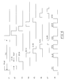
- Fig. 5 represents the drive and logic signals to illuminate rows 1, 4, and 6. Note should be taken that the scan time shown as T10 must be less than 1/30 sec to avoid the appearance of display flicker to the human eye.
- Timax (flicker) 9.625 ⁇ 1/30 sec (persistence of vision).
- T7 should be less than 3.5 msec.
- Fig. 6 represents the drive and logic signals to illuminate rows 1, 4, and 6 using on time compensation. Note should be taken that the period of the logic signals must match the (differing) row pulse widths.
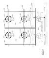
- FIG. 7 A section of a transparent display message center constructed in accordance with the precepts of the present invention is illustrated in Fig. 7.
- ITO coated glass e.g. 1 micron thickness ITO layer
- Associated mesas, 214-220 are laser cut in the ITO to isolate such mesas within their respective columns.
- S Surface mount LEDS
- 230-236 are attached to each mesa 214-220 at one end and to their respective columns at the other end.
- Voltage drives associated with each wire 200 and 202 are not shown, but are provided.
- a laser cut line, 238, terminates the length of column lands 210 and 212.
- the terminal resistance, which can be varied by physical design, of each column land 210, 212, is shown generally by numeral 240.
- FET's, 242 and 244 are associated respectively with column lands 210 and 212.
- the source (S), gate (G), and drain (D) are connected in conventional fashion.
- a ground wire, 246, is electrically coupled to the ITO coated glass by conductive epoxy, such as identified by numerals 248 and 250.
- conductive epoxy such as identified by numerals 248 and 250.
- Logic to FET's 242 and 244 are represented as V1 Logic and V2 logic. The size of each pixel is 0.25" (ignoring kerf).
- the areas of opacity may, for example, come from the FET's (e.g., 244 and it's affixing conductive adhesive spots)and associated LED's (e.g., 232 and 234 and their affixing conductive adhesive spots), , and the row wire conductors ( e.g. , 200, 202).
- the display can achieve a transparency of about 80% or greater.
- the inventive display may utilize widely dispersed, surface mount LED's having dimensions of, for example, about 0.8 mm X 1.6 mm.
- Table 2 below, based on Reference Data for Engineers Seventh Edition Howard Sams & Co Edited by E.C. Jordan, illustrates the apparent opacity resulting when standard thickness copper platings, for example, are etched away leaving a conductor that will carry the required 4.5 A current without fusing at 30 deg. C for a display with 64 columns of LED elements spaced 6 mm ( 240 mil inches) apart.
- the row conductors consist of small 30 gauge wire, which has a diameter of 10 mil inches and a fusing current of over 10 amperes. Using this thin wire, the resulting obscurity would be about 4.1 %.
- the total obscurity caused by the foregoing components will be the sum of the obscurities of the LEDs, their associated dots, and the row conductors.
- the transparency of the display is approximately 88%.
- the LED's, conductive adhesive spots, and row conductors represent opaque areas, these should not objectionably interfere with the otherwise transparent display message center manufactured as shown in Fig. 7.
- the transparent display message center is programmable. Because the display is two-way transparent, the message center may be programmed to display a message viewable from either side of the display. For example, when driven in one direction, the message may be displayed to a viewer observing the front or exterior side of a cooler door. When driven in the opposite direction, the message may be displayed to be a viewer observing the back or interior side of a cooler door, e.g., when viewer has opened the cooler door to examine or remove a product.
- Fig. 8 shows a second and preferred embodiment of a section of a transparent display message center constructed in accordance with the precepts of the present invention.
- the construction of the column and rows in this second embodiment is the same as the construction described in connection with Fig. 7.
- column drives for each column consist of a sinking driver, 291, controlled by a control shift register/latch data, 292, located in a thin, opaque block, 290 , at one edge of the otherwise nearly transparent display. Similar column drivers are associated with each column.
- opaque block 290 detracts somewhat from the otherwise nearly transparent display, block 290 can be positioned over a cooler shelf edge and, thereby still not obscure the produce on display in the cooler. The LED message still appears "magically" in a nearly clear area and the point of purchase attention is gleaned.
Landscapes
- Engineering & Computer Science (AREA)
- Physics & Mathematics (AREA)
- General Physics & Mathematics (AREA)
- Theoretical Computer Science (AREA)
- Computer Hardware Design (AREA)
- Control Of Indicators Other Than Cathode Ray Tubes (AREA)
- Devices For Indicating Variable Information By Combining Individual Elements (AREA)
Applications Claiming Priority (2)
| Application Number | Priority Date | Filing Date | Title |
|---|---|---|---|
| US390211 | 2003-03-17 | ||
| US10/390,211 US20060164333A1 (en) | 2001-01-29 | 2003-03-17 | Transparent programmable LED display panel and method |
Publications (1)
| Publication Number | Publication Date |
|---|---|
| EP1460609A2 true EP1460609A2 (fr) | 2004-09-22 |
Family
ID=32824840
Family Applications (1)
| Application Number | Title | Priority Date | Filing Date |
|---|---|---|---|
| EP03100889A Withdrawn EP1460609A2 (fr) | 2003-03-17 | 2003-04-03 | Procédé et panneau d'affichage transparent et programmable à diodes électroluminescentes |
Country Status (3)
| Country | Link |
|---|---|
| US (1) | US20060164333A1 (fr) |
| EP (1) | EP1460609A2 (fr) |
| CN (1) | CN1530897A (fr) |
Cited By (6)
| Publication number | Priority date | Publication date | Assignee | Title |
|---|---|---|---|---|
| EP1715523A1 (fr) | 2005-04-21 | 2006-10-25 | C.R.F. Società Consortile per Azioni | Dispositif d'affichage transparent à diodes LED |
| EP1715522A1 (fr) | 2005-04-21 | 2006-10-25 | C.R.F. Società Consortile per Azioni | Dispositif d'affichage transparent à diodes LED et son procédé de fabrication |
| EP1918351A3 (fr) * | 2006-10-12 | 2008-07-09 | Lintec Corporation | Feuille luminescente ayant un propriété de visualisation, matériel décoratif luminescent, et procédé de production d'une feuille luminescente |
| EP2037438A1 (fr) * | 2007-09-13 | 2009-03-18 | Dmitrijs Volohovs | Module d'affichage configurant un affichage transparent de grande taille |
| EP2182503A1 (fr) | 2008-11-04 | 2010-05-05 | Electrolux Home Products N.V. | Appareil électroménager |
| US8837120B2 (en) | 2010-12-17 | 2014-09-16 | Bsh Home Appliances Corporation | Transparent display for home appliances |
Families Citing this family (3)
| Publication number | Priority date | Publication date | Assignee | Title |
|---|---|---|---|---|
| US10157316B2 (en) * | 2012-11-05 | 2018-12-18 | Whirlpool Corporation | Interactive touch screen device for wine |
| KR102337353B1 (ko) * | 2014-08-20 | 2021-12-09 | 삼성디스플레이 주식회사 | 투명 표시 패널 및 이를 포함하는 투명 유기 발광 다이오드 표시 장치 |
| US10957284B1 (en) | 2019-10-30 | 2021-03-23 | Kristi Nay | Changeable holiday display |
Family Cites Families (6)
| Publication number | Priority date | Publication date | Assignee | Title |
|---|---|---|---|---|
| US3757322A (en) * | 1971-02-03 | 1973-09-04 | Hall Barkan Instr Inc | Transparent touch controlled interface with interreactively related display |
| US4549918A (en) * | 1982-10-08 | 1985-10-29 | Sanders Associates, Inc. | Precision wire grid glass digitizing tablets |
| US5184114A (en) * | 1982-11-04 | 1993-02-02 | Integrated Systems Engineering, Inc. | Solid state color display system and light emitting diode pixels therefor |
| US5623201A (en) * | 1993-09-28 | 1997-04-22 | Samsung Electronics Co., Ltd. | 3-phase power meter having a display board |
| JPH07253594A (ja) * | 1994-03-15 | 1995-10-03 | Fujitsu Ltd | 表示装置 |
| US5896575A (en) * | 1997-02-28 | 1999-04-20 | Motorola, Inc. | Electronic device with display viewable from two opposite ends |
-
2003
- 2003-03-17 US US10/390,211 patent/US20060164333A1/en not_active Abandoned
- 2003-04-03 EP EP03100889A patent/EP1460609A2/fr not_active Withdrawn
-
2004
- 2004-02-24 CN CNA2004100059980A patent/CN1530897A/zh active Pending
Cited By (9)
| Publication number | Priority date | Publication date | Assignee | Title |
|---|---|---|---|---|
| EP1715523A1 (fr) | 2005-04-21 | 2006-10-25 | C.R.F. Società Consortile per Azioni | Dispositif d'affichage transparent à diodes LED |
| EP1715522A1 (fr) | 2005-04-21 | 2006-10-25 | C.R.F. Società Consortile per Azioni | Dispositif d'affichage transparent à diodes LED et son procédé de fabrication |
| US7884784B2 (en) | 2005-04-21 | 2011-02-08 | C.R.F. Societa Consortile Per Azioni | Transparent LED display |
| US7932524B2 (en) | 2005-04-21 | 2011-04-26 | C.R.F. Societa Consortile Per Azioni | Transparent LED display and method for manufacture thereof |
| EP1918351A3 (fr) * | 2006-10-12 | 2008-07-09 | Lintec Corporation | Feuille luminescente ayant un propriété de visualisation, matériel décoratif luminescent, et procédé de production d'une feuille luminescente |
| US8758883B2 (en) | 2006-10-12 | 2014-06-24 | Lintec Corporation | Luminescent sheet having see-through property, luminescent decorative material, and method of producing luminescent sheet |
| EP2037438A1 (fr) * | 2007-09-13 | 2009-03-18 | Dmitrijs Volohovs | Module d'affichage configurant un affichage transparent de grande taille |
| EP2182503A1 (fr) | 2008-11-04 | 2010-05-05 | Electrolux Home Products N.V. | Appareil électroménager |
| US8837120B2 (en) | 2010-12-17 | 2014-09-16 | Bsh Home Appliances Corporation | Transparent display for home appliances |
Also Published As
| Publication number | Publication date |
|---|---|
| US20060164333A1 (en) | 2006-07-27 |
| CN1530897A (zh) | 2004-09-22 |
Similar Documents
| Publication | Publication Date | Title |
|---|---|---|
| EP1460609A2 (fr) | Procédé et panneau d'affichage transparent et programmable à diodes électroluminescentes | |
| US4948232A (en) | Device for the presentation of information with rollable plastic substrate | |
| US6379209B1 (en) | Alpha-numeric character display panel | |
| US20040256977A1 (en) | Overlapping array display | |
| US20140331532A1 (en) | Flexible clear and transparent lighting strips and signage | |
| US10573230B2 (en) | Backlight source, display device and driving method thereof | |
| WO2007055457A1 (fr) | Panneau electrique transparent et del de puce associee | |
| CA2246761A1 (fr) | Appareil d'eclairage pour presentoir | |
| CN110660837A (zh) | 显示面板及显示装置 | |
| KR20150015606A (ko) | 유기 발광 표시장치 | |
| KR20130069309A (ko) | 유기 전계 발광 표시장치 | |
| US20020149547A1 (en) | Transparent programmable LED display panel and method | |
| KR102162880B1 (ko) | 투명 디지털 사이니지 디스플레이 및 그를 위한 선 저항이 감소된 인쇄회로기판 | |
| JP4637513B2 (ja) | 表示装置およびその駆動方法 | |
| KR102882181B1 (ko) | 표시 장치 | |
| US20200133085A1 (en) | Liquid crystal display device | |
| KR102534079B1 (ko) | 표시 장치 | |
| CN108091668B (zh) | 有机发光显示屏及有机发光显示组件 | |
| US11735700B2 (en) | Display device | |
| JP3210219U (ja) | 看板装置 | |
| DE29606511U1 (de) | Elektrolumineszenzleuchtflächen auf transparenter Platte mit nicht sichtbarer Kontaktierung | |
| KR102953048B1 (ko) | 양방향 시인성을 가지는 투명 표시장치 | |
| JP7285538B2 (ja) | 透過性制御ディスプレイ、透過性制御ディスプレイ付ホームドア及び車両用透過性制御ディスプレイ | |
| KR20220050284A (ko) | 표시 장치 | |
| US20250378778A1 (en) | Micro-led panel, operating method thereof and pixel compensation circuit |
Legal Events
| Date | Code | Title | Description |
|---|---|---|---|
| PUAI | Public reference made under article 153(3) epc to a published international application that has entered the european phase |
Free format text: ORIGINAL CODE: 0009012 |
|
| AK | Designated contracting states |
Kind code of ref document: A2 Designated state(s): AT BE BG CH CY CZ DE DK EE ES FI FR GB GR HU IE IT LI LU MC NL PT RO SE SI SK TR |
|
| AX | Request for extension of the european patent |
Extension state: AL LT LV MK |
|
| STAA | Information on the status of an ep patent application or granted ep patent |
Free format text: STATUS: THE APPLICATION IS DEEMED TO BE WITHDRAWN |
|
| 18D | Application deemed to be withdrawn |
Effective date: 20051101 |