EP1460686A2 - Procédé de fabrication d'une résistance à couche mince dans une structure à double damasquinage - Google Patents
Procédé de fabrication d'une résistance à couche mince dans une structure à double damasquinage Download PDFInfo
- Publication number
- EP1460686A2 EP1460686A2 EP04101105A EP04101105A EP1460686A2 EP 1460686 A2 EP1460686 A2 EP 1460686A2 EP 04101105 A EP04101105 A EP 04101105A EP 04101105 A EP04101105 A EP 04101105A EP 1460686 A2 EP1460686 A2 EP 1460686A2
- Authority
- EP
- European Patent Office
- Prior art keywords
- thin film
- film resistor
- dielectric layer
- trench
- forming
- Prior art date
- Legal status (The legal status is an assumption and is not a legal conclusion. Google has not performed a legal analysis and makes no representation as to the accuracy of the status listed.)
- Ceased
Links
Images


Classifications
-
- H—ELECTRICITY
- H10—SEMICONDUCTOR DEVICES; ELECTRIC SOLID-STATE DEVICES NOT OTHERWISE PROVIDED FOR
- H10D—INORGANIC ELECTRIC SEMICONDUCTOR DEVICES
- H10D1/00—Resistors, capacitors or inductors
- H10D1/40—Resistors
- H10D1/47—Resistors having no potential barriers
-
- H—ELECTRICITY
- H10—SEMICONDUCTOR DEVICES; ELECTRIC SOLID-STATE DEVICES NOT OTHERWISE PROVIDED FOR
- H10W—GENERIC PACKAGES, INTERCONNECTIONS, CONNECTORS OR OTHER CONSTRUCTIONAL DETAILS OF DEVICES COVERED BY CLASS H10
- H10W20/00—Interconnections in chips, wafers or substrates
- H10W20/01—Manufacture or treatment
-
- H—ELECTRICITY
- H10—SEMICONDUCTOR DEVICES; ELECTRIC SOLID-STATE DEVICES NOT OTHERWISE PROVIDED FOR
- H10W—GENERIC PACKAGES, INTERCONNECTIONS, CONNECTORS OR OTHER CONSTRUCTIONAL DETAILS OF DEVICES COVERED BY CLASS H10
- H10W20/00—Interconnections in chips, wafers or substrates
- H10W20/40—Interconnections external to wafers or substrates, e.g. back-end-of-line [BEOL] metallisations or vias connecting to gate electrodes
- H10W20/498—Resistive arrangements or effects of, or between, wiring layers
Definitions
- the invention is generally related to the field of thin film resistors and more specifically to a method of forming a thin film resistor in a dual damascene structure with copper interconnects.
- Thin film resistors are very attractive components for high precision analog and mixed signal applications. In addition to a low thermal coefficient of resistance, low voltage coefficient of resistance, and good resistor matching they should provide good stability under stress.
- Integrated circuit copper interconnects are formed using damascene processes.
- a damascene process a trench is first formed in a dielectric layer.
- the trench is then filled with copper and the excess copper is removed by a number of methods including chemical mechanical polishing.
- the formation of thin film resistors in an integrated cir cuit containing copper interconnects presents many challenges.
- the thin film resistor is not formed using copper and so is incompatible with existing damascene processes.
- the incompatibility is exacerbated by the requirement that the thin film resistors be formed in the same levels as the copper interconnects. There is therefore a need for a method to form thin film resistors in integrated circuits with copper interconnects formed using damascene processes.
- the instant invention describes a method for integrating a thin film resistor into an integrated circuit comprising copper interconnects formed using dual damascene structures.
- an etch stop layer is formed on a dielectric layer.
- a thin film resistor is formed over the etch stop layer and contact pads are formed on the thin film resistor.
- a second dielectric layer is formed over the thin film resistor and at least one trench is formed in the second dielectric layer.
- thin film resistor vias are formed above the contact pads on the thin film resistor.
- a via trench is formed in the trench structure and metal is formed in the trench, via trench, and thin film resistor vias.
- FIG. 1 (a) An embodiment of the instant invention is shown in Figure 1 (a) - Figure 1 (f) .
- a metal interconnect 20 is formed over a dielectric layer 10.
- the dielectric layer 10 is formed over a semiconductor substrate and any number of intervening layers.
- the semiconductor and any intervening layers have been omitted from the Figures for clarity.
- the layers beneath the dielectric layer 10 will comprise any number of active devices including MOS and/or bipolar transistors as well as any number of metal interconnect levels.
- an inter-level dielectric layer 30 is formed over the metal interconnect layer 20.
- the inter -level dielectric layer 30 can comprise silicon oxide formed using any suitable method including chemical vapor deposition.
- the inter-level dielectric layer 30 is formed using material selected from the group comprising TEOS silicon oxides, PECVD silicon oxides, silicon nitrides, silicon oxynitrides, silicon carbides, spin-on glass (SOG) such as silsesquioxanes and siloxane, xerogels or any other suitable material.
- SOG spin-on glass
- an etch stop layer 40 is formed over the inter-level dielectric layer 30.
- the etch stop layer 40 can comprise silicon nitride, silicon carbide, silicon oxynitride, combinations of one or all of these and other suitable layers, and any other suitable dielectric material.
- a thin film resistor layer 50 is then formed over the etch stop layer 40. In subsequent processing the resistor layer 50 will be etched to form the thin film resistor (TFR).
- the resistor layer 50 is formed using a silicon chromium (SiCr) alloy, nickel chromium (NiCr) alloy, tantalum nitride, titanium nitride, tungsten, or any other suitable material.
- a photoresist layer 58 is formed and patterned over the thin film resistor layer 50 and will be used to define the TFR during the etching process.
- FIG. 1 (b) Shown in Figure 1 (b) is the TFR 55 formed by etching the resistor layer 50 using the photoresist layer 58 shown in Figure 1(a) as a masking layer.
- the resistor layer 50 can be etched using any suitable dry or wet etching process.
- a conductive contact layer 60 is formed over the TFR structure 55.
- the conductive contact layer 60 is formed using titanium nitride, titanium tungsten, or any other suitable conductive material.
- the conductive contact layer 60 can comprise multiple layers formed using layers comprised of the same or differing conductive material.
- patterned photoresist 70 is formed over the capping layer as shown in Figure 1 (b) and will be used to pattern the contact layer 60.
- inter-level dielectric layer 80 is formed over the TFR 55.
- the inter-level dielectric layer 80 can comprise silicon oxide formed using any suitable method including chemical vapor deposition.
- the inter-level dielectric layer 80 is formed using material selected from the group comprising TEOS silicon oxides, PECVD silicon oxides, silicon nitrides, silicon oxynitrides, silicon carbides, spin-on glass (SOG) such as silsesquioxanes and siloxane, xerogels or any other suitable material.
- patterned photoresist layers 90 are formed on the inter-level dielectric layer 80.
- the patterned photoresist layers 90 will function as etch masks during the subsequent etching of vias and trenches in the dielectric layer 80.
- FIG. 1(d) Shown in Figure 1(d) is the structure of Figure 1(c) following the simultaneous etching of TFR vias 92 and a trench 94 in the inter-level dielectric layer 80.
- TFR and trench are shown in the Figure, it should be noted that the method of the instant invention could be used to form any number of trench and via structures in the dielectric layer in addition to the TFR vias.
- a via will be used in the instant invention to describe a structure that contacts an underlying conductive layer such as a TFR, a metal interconnect, or an electronic device.
- a trench will be used to describe the structure formed in the dielectric lay er in which a metal interconnect line will be formed.
- the etching of the inter -level dielectric layer 80 in Figure 1 (d) is performed using a dry etch process that is designed to stop on the etch stop layer 40.
- a dry etch process that is designed to stop on the etch stop layer 40.
- any dry etch process with high silicon oxide to silicon nitride selectivity can be used.
- the contact pads 65 will protect the regions of the TFR 55 that would have been exposed to the etch process.
- the etch process used should therefore also have high selectivity between the dielectric layer 80 and the contact pads 65.
- the etched TFR vias 92 will be used to provide electrical contact to the TFR 55 and a copper interconnect metal line will be formed in the trench structure 94.
- a patterned photoresist layer 100 is formed and used as a mask during the formation of t he trench via 96.
- the trench via 96 is formed by etching through the etch stop layer 40 and the underlying dielectric layer 30.
- the photoresist layer 100 is removed and metal 120 and 11 0 is formed in the TFR vias and the trench and trench via respectively.
- the metal formed can comprise copper or any other suitable metal.
- 120 and 110 can be formed using any known integrated circuit processing method including copper metal deposition and chemical mechanical polishing.
- the integrated circuit can be completed using known manufacturing methods.
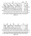
- FIG. 2(a)- Figure 2(d) A further embodiment of the instant invention is shown in Figure 2(a)- Figure 2(d). Shown in Figure 2(a) is a metal interconnect 20 is formed over a dielectric layer 10. An inter-level dielectric layer 30 is formed on the metal interconnect layer 10.
- the inter-level dielectric layer 30 can comprise silicon oxide formed using any suitable method including chemical vapor deposition.
- the inter-level dielectric layer 30 is formed using material selected from the group comprising TEOS silicon oxides, PECVD silicon oxides, silicon nitrides, silicon oxynitrides, silicon carbides, spin -on glass (SOG) such as silsesquioxanes and siloxane, xerogels or any other suitable material.
- SOG spin -on glass
- the resistor layer is formed using a silicon chromium (SiCr) alloy, nickel chromium (NiCr) alloy, tantalum nitride, titanium nitride, tungsten, or any other suitable material.
- an inter-level dielectric layer 80 is formed over the TFR 55.
- the inter-level dielectric layer 80 can comprise silicon oxide formed using any suitable method including chemical vapor deposition.
- the inter-level dielectric layer 80 is formed using material selected from the group comprising TEOS silicon oxides, PECVD silicon oxides, silicon nitrides, silicon oxynitrides, silicon carbides, spin-on glass (SOG) such as silsesquioxanes and siloxane, xerogels or any other suitable material.
- patterned photoresist layers 90 are formed on the dielectric layer 80. The patterned photoresist layers 90 will function as etch masks during the subsequent etching of trenches in the dielectric layer 80.
- FIG. 2(b) Shown in Figure 2(b) is the structure of Figure 2(a) following the simultaneous etching of TFR vias 92 and the trench 94 in the dielectric layer 80.
- the etching of the inte r-level dielectric layer 80 in Figure 2(b) is performed using a timed dry etch process that is designed to stop upon etching through the dielectric layer 80. It is not critical that the etch process stop immediately at the interface between the dielectric layers 80 and 30. It is however important that the contact pads 65 be exposed following the etch process. During the etching of the inter -level dielectric layer 80, the contact pads 65 will protect the regions of the TFR 55 that would have been exposed to the etch process. This implies that the etch process used should also have high selectivity between the dielectric layer 80 and the contact pads 65.
- the etched TFR vias 92 will be used to provide electrical contact to the TFR 55 and a copper interconnect will be formed in the trench structure 94.
- a patterned photoresist layer 100 is formed and used as a mask during the formation of the trench via 96.
- the trench via 96 is formed by etching through the etch stop layer 40 and the underlying inter-level dielectric layer 30.
- the photoresist layer 100 is removed and copper metal 120 and 110 is formed in the TFR vias, the trench, and the trench via.
- the copper metal 120 and 110 can be formed using any known integrated circuit processing method including copper metal deposition and chemical mechanical polishing. Following the formation of the structure shown in Figure 2(d), the integrated circuit can be completed using known manufacturing methods.
Landscapes
- Internal Circuitry In Semiconductor Integrated Circuit Devices (AREA)
- Semiconductor Integrated Circuits (AREA)
Applications Claiming Priority (2)
| Application Number | Priority Date | Filing Date | Title |
|---|---|---|---|
| US10/390,054 US6734076B1 (en) | 2003-03-17 | 2003-03-17 | Method for thin film resistor integration in dual damascene structure |
| US390054 | 2003-03-17 |
Publications (2)
| Publication Number | Publication Date |
|---|---|
| EP1460686A2 true EP1460686A2 (fr) | 2004-09-22 |
| EP1460686A3 EP1460686A3 (fr) | 2008-09-17 |
Family
ID=32230105
Family Applications (1)
| Application Number | Title | Priority Date | Filing Date |
|---|---|---|---|
| EP04101105A Ceased EP1460686A3 (fr) | 2003-03-17 | 2004-03-17 | Procédé de fabrication d'une résistance à couche mince dans une structure à double damasquinage |
Country Status (3)
| Country | Link |
|---|---|
| US (1) | US6734076B1 (fr) |
| EP (1) | EP1460686A3 (fr) |
| JP (1) | JP2004282081A (fr) |
Families Citing this family (17)
| Publication number | Priority date | Publication date | Assignee | Title |
|---|---|---|---|---|
| US7323751B2 (en) * | 2003-06-03 | 2008-01-29 | Texas Instruments Incorporated | Thin film resistor integration in a dual damascene structure |
| US7291525B1 (en) * | 2004-08-05 | 2007-11-06 | National Semiconductor Corporation | System and method for manufacturing thin film resistors using a trench and chemical mechanical polishing |
| US7064414B2 (en) * | 2004-11-12 | 2006-06-20 | International Business Machines Corporation | Heater for annealing trapped charge in a semiconductor device |
| US7211494B2 (en) * | 2004-12-28 | 2007-05-01 | Medtronic, Inc. | Semiconductor structures utilizing thin film resistors and tungsten plug connectors and methods for making the same |
| KR100599949B1 (ko) | 2004-12-30 | 2006-07-12 | 매그나칩 반도체 유한회사 | 반도체 소자의 박막 레지스터 제조 방법 |
| KR100667915B1 (ko) | 2004-12-30 | 2007-01-11 | 매그나칩 반도체 유한회사 | 반도체 소자의 박막 레지스터 형성 방법 |
| KR101159113B1 (ko) * | 2005-04-29 | 2012-06-25 | 매그나칩 반도체 유한회사 | 반도체 소자의 제조방법 |
| US7485540B2 (en) * | 2005-08-18 | 2009-02-03 | International Business Machines Corporation | Integrated BEOL thin film resistor |
| US7829428B1 (en) | 2008-08-26 | 2010-11-09 | National Semiconductor Corporation | Method for eliminating a mask layer during thin film resistor manufacturing |
| DE102010008942B4 (de) * | 2010-02-23 | 2019-07-11 | Texas Instruments Deutschland Gmbh | Verfahren für eine vereinfachte Integration von hochgenauen Dünnfilmwiderständen |
| US8400257B2 (en) * | 2010-08-24 | 2013-03-19 | Stmicroelectronics Pte Ltd | Via-less thin film resistor with a dielectric cap |
| CN102324427B (zh) * | 2011-10-20 | 2016-03-16 | 上海集成电路研发中心有限公司 | 一种金属薄膜电阻结构及其制造方法 |
| US9502284B2 (en) | 2013-12-31 | 2016-11-22 | Texas Instruments Incorporated | Metal thin film resistor and process |
| US10211278B2 (en) * | 2017-07-11 | 2019-02-19 | Texas Instruments Incorporated | Device and method for a thin film resistor using a via retardation layer |
| CN111009512A (zh) * | 2018-10-08 | 2020-04-14 | 无锡华润上华科技有限公司 | 薄膜电阻的制造方法和薄膜电阻 |
| US11315876B2 (en) | 2020-02-17 | 2022-04-26 | Globalfoundries Singapore Pte. Ltd. | Thin film conductive material with conductive etch stop layer |
| CN120752713A (zh) * | 2022-12-22 | 2025-10-03 | 绿源制造有限公司 | 选择性薄膜电阻器及其制造方法 |
Citations (1)
| Publication number | Priority date | Publication date | Assignee | Title |
|---|---|---|---|---|
| US6500724B1 (en) * | 2000-08-21 | 2002-12-31 | Motorola, Inc. | Method of making semiconductor device having passive elements including forming capacitor electrode and resistor from same layer of material |
Family Cites Families (11)
| Publication number | Priority date | Publication date | Assignee | Title |
|---|---|---|---|---|
| US3988824A (en) * | 1972-05-22 | 1976-11-02 | Hewlett-Packard Company | Method for manufacturing thin film circuits |
| JP3404064B2 (ja) * | 1993-03-09 | 2003-05-06 | 株式会社日立製作所 | 半導体装置及びその製造方法 |
| US5874770A (en) * | 1996-10-10 | 1999-02-23 | General Electric Company | Flexible interconnect film including resistor and capacitor layers |
| US5976943A (en) * | 1996-12-27 | 1999-11-02 | Vlsi Technology, Inc. | Method for bi-layer programmable resistor |
| JPH10303372A (ja) * | 1997-01-31 | 1998-11-13 | Sanyo Electric Co Ltd | 半導体集積回路およびその製造方法 |
| US6921962B1 (en) * | 1998-12-18 | 2005-07-26 | Texas Instruments Incorporated | Integrated circuit having a thin film resistor located within a multilevel dielectric between an upper and lower metal interconnect layer |
| US6235628B1 (en) * | 1999-01-05 | 2001-05-22 | Advanced Micro Devices, Inc. | Method of forming dual damascene arrangement for metal interconnection with low k dielectric constant materials and oxide middle etch stop layer |
| US6313003B1 (en) * | 2000-08-17 | 2001-11-06 | Taiwan Semiconductor Manufacturing Company | Fabrication process for metal-insulator-metal capacitor with low gate resistance |
| US6426268B1 (en) * | 2000-11-28 | 2002-07-30 | Analog Devices, Inc. | Thin film resistor fabrication method |
| US6943414B2 (en) * | 2001-03-15 | 2005-09-13 | Newport Fab, Llc | Method for fabricating a metal resistor in an IC chip and related structure |
| US6534374B2 (en) * | 2001-06-07 | 2003-03-18 | Institute Of Microelectronics | Single damascene method for RF IC passive component integration in copper interconnect process |
-
2003
- 2003-03-17 US US10/390,054 patent/US6734076B1/en not_active Expired - Lifetime
-
2004
- 2004-03-16 JP JP2004073661A patent/JP2004282081A/ja active Pending
- 2004-03-17 EP EP04101105A patent/EP1460686A3/fr not_active Ceased
Patent Citations (1)
| Publication number | Priority date | Publication date | Assignee | Title |
|---|---|---|---|---|
| US6500724B1 (en) * | 2000-08-21 | 2002-12-31 | Motorola, Inc. | Method of making semiconductor device having passive elements including forming capacitor electrode and resistor from same layer of material |
Also Published As
| Publication number | Publication date |
|---|---|
| EP1460686A3 (fr) | 2008-09-17 |
| JP2004282081A (ja) | 2004-10-07 |
| US6734076B1 (en) | 2004-05-11 |
Similar Documents
| Publication | Publication Date | Title |
|---|---|---|
| US7323751B2 (en) | Thin film resistor integration in a dual damascene structure | |
| US6734076B1 (en) | Method for thin film resistor integration in dual damascene structure | |
| US6825092B2 (en) | Semiconductor device having passive elements and method of making same | |
| US10177214B2 (en) | Metal thin film resistor and process | |
| US8013394B2 (en) | Integrated circuit having resistor between BEOL interconnect and FEOL structure and related method | |
| US6872655B2 (en) | Method of forming an integrated circuit thin film resistor | |
| US7960240B1 (en) | System and method for providing a dual via architecture for thin film resistors | |
| CN107750390B (zh) | 具有增加的掩模层的镶嵌薄膜电阻器 | |
| US10818748B2 (en) | Thin-film resistor (TFR) formed under a metal layer and method of fabrication | |
| US20080132056A1 (en) | INTEGRATION OF THIN FILM RESISTORS HAVING DIFFERENT TCRs INTO SINGLE DIE | |
| US7808048B1 (en) | System and method for providing a buried thin film resistor having end caps defined by a dielectric mask | |
| EP1168432A2 (fr) | Méthode d'intégration d'une résistance en couches minces dans une structure d'interconnection multicouches de Tungstene | |
| US6607962B2 (en) | Globally planarized backend compatible thin film resistor contact/interconnect process | |
| US20020132442A1 (en) | Method for fabricating a metal resistor in an IC chip and related structure | |
| US6855585B1 (en) | Integrating multiple thin film resistors | |
| CN111033718A (zh) | 用于使用通孔阻滞层的薄膜电阻器的装置和方法 | |
| US20090200674A1 (en) | Structure and method of forming transitional contacts between wide and thin beol wirings | |
| EP4682915A1 (fr) | Résistance à couche mince avec structure de barre d'interconnexion | |
| KR101087183B1 (ko) | 반도체 소자의 박막 레지스터 형성방법 | |
| KR20110078953A (ko) | 반도체 소자의 박막 저항 제조방법 | |
| KR20060068289A (ko) | 반도체소자의 레지스터 형성방법 |
Legal Events
| Date | Code | Title | Description |
|---|---|---|---|
| PUAI | Public reference made under article 153(3) epc to a published international application that has entered the european phase |
Free format text: ORIGINAL CODE: 0009012 |
|
| AK | Designated contracting states |
Kind code of ref document: A2 Designated state(s): AT BE BG CH CY CZ DE DK EE ES FI FR GB GR HU IE IT LI LU MC NL PL PT RO SE SI SK TR |
|
| AX | Request for extension of the european patent |
Extension state: AL LT LV MK |
|
| PUAL | Search report despatched |
Free format text: ORIGINAL CODE: 0009013 |
|
| AK | Designated contracting states |
Kind code of ref document: A3 Designated state(s): AT BE BG CH CY CZ DE DK EE ES FI FR GB GR HU IE IT LI LU MC NL PL PT RO SE SI SK TR |
|
| AX | Request for extension of the european patent |
Extension state: AL LT LV MK |
|
| 17P | Request for examination filed |
Effective date: 20090317 |
|
| AKX | Designation fees paid |
Designated state(s): DE FR GB |
|
| 17Q | First examination report despatched |
Effective date: 20090609 |
|
| RBV | Designated contracting states (corrected) |
Designated state(s): DE FR GB NL |
|
| APBK | Appeal reference recorded |
Free format text: ORIGINAL CODE: EPIDOSNREFNE |
|
| APBN | Date of receipt of notice of appeal recorded |
Free format text: ORIGINAL CODE: EPIDOSNNOA2E |
|
| APAF | Appeal reference modified |
Free format text: ORIGINAL CODE: EPIDOSCREFNE |
|
| APBT | Appeal procedure closed |
Free format text: ORIGINAL CODE: EPIDOSNNOA9E |
|
| STAA | Information on the status of an ep patent application or granted ep patent |
Free format text: STATUS: THE APPLICATION HAS BEEN REFUSED |
|
| 18R | Application refused |
Effective date: 20190815 |