EP1460697A2 - Organische elektrolumineszente Anzeigevorrichtung und Herstellungsverfahren - Google Patents
Organische elektrolumineszente Anzeigevorrichtung und Herstellungsverfahren Download PDFInfo
- Publication number
- EP1460697A2 EP1460697A2 EP04251435A EP04251435A EP1460697A2 EP 1460697 A2 EP1460697 A2 EP 1460697A2 EP 04251435 A EP04251435 A EP 04251435A EP 04251435 A EP04251435 A EP 04251435A EP 1460697 A2 EP1460697 A2 EP 1460697A2
- Authority
- EP
- European Patent Office
- Prior art keywords
- film
- organic electroluminescence
- organic
- high molecular
- molecular compound
- Prior art date
- Legal status (The legal status is an assumption and is not a legal conclusion. Google has not performed a legal analysis and makes no representation as to the accuracy of the status listed.)
- Withdrawn
Links
Images

Classifications
-
- H—ELECTRICITY
- H10—SEMICONDUCTOR DEVICES; ELECTRIC SOLID-STATE DEVICES NOT OTHERWISE PROVIDED FOR
- H10K—ORGANIC ELECTRIC SOLID-STATE DEVICES
- H10K59/00—Integrated devices, or assemblies of multiple devices, comprising at least one organic light-emitting element covered by group H10K50/00
- H10K59/80—Constructional details
- H10K59/87—Passivation; Containers; Encapsulations
- H10K59/873—Encapsulations
- H10K59/8731—Encapsulations multilayered coatings having a repetitive structure, e.g. having multiple organic-inorganic bilayers
-
- H—ELECTRICITY
- H10—SEMICONDUCTOR DEVICES; ELECTRIC SOLID-STATE DEVICES NOT OTHERWISE PROVIDED FOR
- H10K—ORGANIC ELECTRIC SOLID-STATE DEVICES
- H10K50/00—Organic light-emitting devices
- H10K50/80—Constructional details
- H10K50/84—Passivation; Containers; Encapsulations
- H10K50/844—Encapsulations
- H10K50/8445—Encapsulations multilayered coatings having a repetitive structure, e.g. having multiple organic-inorganic bilayers
-
- H—ELECTRICITY
- H10—SEMICONDUCTOR DEVICES; ELECTRIC SOLID-STATE DEVICES NOT OTHERWISE PROVIDED FOR
- H10K—ORGANIC ELECTRIC SOLID-STATE DEVICES
- H10K59/00—Integrated devices, or assemblies of multiple devices, comprising at least one organic light-emitting element covered by group H10K50/00
- H10K59/10—OLED displays
- H10K59/17—Passive-matrix OLED displays
Definitions
- the present invention relates to an organic electroluminescence element (hereinafter referred to as an 'organic EL element') that includes one or more thin films each having a light emission layer (hereinafter referred to as 'organic functional layers').
- the light emission layer is made from an organic compound material that exhibits electroluminescence in which light emission takes place due to application (injection) of a current.
- the present invention also relates to an organic electroluminescence display panel (hereinafter referred to as an 'organic EL display panel' ) having a substrate and one or more Organic EL elements formed on the substrate.
- an organic electroluminescence display panel hereinafter referred to as an 'organic EL display panel'
- an organic EL element is formed such that an organic functional layer is interposed between an anode and a cathode.
- Excitons are formed when electrons and positive holes that are implanted from the electrodes (i.e., the cathode and anode) are recombined.
- the organic EL element generates light when the excitons return to a base state from an excited state.
- an organic EL element is formed by sequentially laminating a transparent electrode constituting an anode, an organic functional layer, and a metal electrode constituting a cathode, on a transparent substrate, and light emission is obtained from the transparent substrate side.
- the organic functional layer is a single-layer light emission layer or is a laminate body with a three-layer structure consisting of an organic positive hole carrier layer, a light emission layer and an organic electron carrier layer, or a two-layer structure consisting of an organic positive hole carrier layer and light emission layer.
- An electron or positive-hole injection layer and/or a carrier block layer is sometimes inserted between suitable layers of the aforementioned layers.
- organic EL display panels include the matrix display type and those having a predetermined light emission pattern.
- the organic EL elements When exposed to the atmosphere, these organic EL elements degrade readily under the effects of moisture, gases such as oxygen, and other molecules of a certain type in a given environment. Characteristic degradation is particularly prominent at the interfaces between the electrodes of the organic EL element and the organic functional layer. The characteristic degradation often causes a drop in light emission characteristics such as luminance, color, and so forth.
- the organic EL element In order to prevent the characteristic degradation of the organic EL display panel, the organic EL element is sealed by means of an inorganic single-layer protective film of silicon oxide or the like. However, such a protective film does not possess adequate barrier properties. This is because the generation of pinholes in the inorganic barrier film (protective film) is unavoidable. When pinholes exist in the protective film, moisture, oxygen, and so forth penetrate into the organic EL element via the pinholes, resulting in expansion of so-called dark spots in the organic EL element. No light emission occurs in the dark spots.
- One object of the present invention is to provide an organic EL element in which an organic functional layer and electrodes are afforded the property of high insulation with respect to oxygen and moisture and so forth, so that the degradation of light emission characteristics does not readily occur.
- Another object of the present invention is to provide an organic EL display panel that can prevent penetration of oxygen, moisture and the like.
- a novel organic EL display panel having a plurality of organic EL elements.
- Each organic EL element of the display panel includes first and second display electrodes and one or more organic functional layers.
- the organic functional layer includes an organic compound and is laminated between the first and second display electrodes.
- the display panel also includes a substrate for supporting the organic EL elements.
- a high molecular compound film made of polyurea or polyimide, for example, is provided over the organic EL elements on the substrate to cover the organic EL elements and their peripheral areas on the substrate surface.
- An inorganic barrier film is also provided to cover the high molecular compound film, its edge face, and its peripheral substrate surface. It should be noted that the inorganic barrier film may be formed over the organic EL element, and then the high molecular compound film may be formed on the inorganic barrier film.
- a method of fabricating an organic EL display panel First, a substrate is prepared. Then, at least one organic EL element is formed on the substrate. Each organic EL element has first and second display electrodes and at least one organic functional layer made from an organic compound. The organic functional layer is laminated between the first and second display electrodes. A first sealing film is deposited over the organic EL element. The first sealing film has a larger area than the organic EL element so as to cover the organic EL element and a peripheral area of the organic EL element on the substrate. A second sealing film is deposited over the first sealing film.
- the second sealing film has a larger area than the first sealing film so as to cover the first sealing film, an edge portion of the first sealing film, and a peripheral area of the first sealing film on the substrate.
- the first sealing film may be a high molecular compound film, made from polyurea or polyimide
- the second sealing film may be an inorganic barrier film.
- the first sealing film may be an inorganic barrier film
- the second sealing film may be a high molecular compound film, made from polyurea or polyimide.
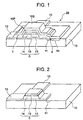
- an organic EL device 28 of this embodiment includes a substrate 10, a first display electrode 13 (transparent electrode anode), one or more organic functional layers 14 each having a light emission layer made of an organic compound, and a second display electrode 15 (metal electrode cathode), which are sequentially deposited on the substrate 10.
- the combination of the first display electrode 13, organic functional layer(s) 14 and second display electrode 15 is referred to as an organic EL element D in this specification.
- the substrate 10 is made of glass or the like.
- the organic EL device 28 also includes a multi-layer sealing part made from two films, i.e., a high molecular compound film 16P and an inorganic barrier film 16S which are laminated in this order, to cover the top surface of the second display electrode 15.
- the high molecular compound film 16P is a polyurea or polyimide film formed by vapor deposition polymerization.
- the high molecular compound film 16P covers the organic EL element D and its peripheral area (surface) R1 on the substrate 10.
- the inorganic barrier film 16S covers the high molecular compound film 16P, its edge portion E, and its peripheral area (surface) R2 on the substrate 10.
- the edge face E of the high molecular compound film 16P is formed having a film thickness that gradually decreases (or a tapered shape) in order to secure smooth or easy deposition of the inorganic barrier film 16S.
- There are no limitations on the material of the substrate 10 so that an organic material such as a high molecular compound may be used for the substrate 10, or an inorganic material such as glass may be used for the substrate 10.
- the organic EL element D has, over itself, a multi-layered deposition structure consisting of the inorganic barrier film 16S and the high molecular compound film 16P.
- the reversed deposition order is acceptable for the inorganic barrier film 16S and the high molecular compound film 16P, i.e., the barrier film 16S may be formed on the organic EL element D, and the high molecular compound film 16P may be formed over the barrier film 16S.
- the organic EL device 28 is fabricated by means of the following procedure.
- the first display electrode 13 which is made of indium tin oxide (ITO), is deposited on the substrate 10 by means of vapor deposition or sputtering. Subsequently, a predetermined pattern is formed by means of a photolithographic process.
- the organic functional layer 14 is formed by using vapor deposition to sequentially deposit, on top of this predetermined pattern, a positive hole injection layer made of copper phthalocyanine, a positive hole carrier layer made of TPD (triphenylamine derivative), a light emission layer made of an Alq3 (aluminum chelate complex), and an electron injection layer made of Li 2 O (lithium oxide).
- the second display electrode 15 made of Al is deposited, by means of vapor deposition, on top of the organic functional layer 14 to face the electrode pattern of the transparent electrode 13 via the organic functional layer 14.
- a polyurea or polyimide film is deposited by means of vapor deposition polymerization as the high molecular compound film 16P atop the organic EL element D.
- the vapor deposition polymerization is carried out within a vacuum chamber of a vapor deposition polymerization device (not shown).
- the high molecular compound film 16P is deposited over a larger area than a display region containing a pixel or organic EL element D by using a first mask M1.
- the first mask M1 has an opening of predetermined shape for passage of a aterial of the high molecular compound film 16P.
- Gas within the high molecular compound film 16P is removed by annealing the polyurea or polyimide film 16P deposited on the organic EL element D at or below a temperature (about 100°C) of a magnitude so as not to damage the organic functional layer 14 in a vacuum or an inert gas such as N 2 . Then, the inorganic film 16S is deposited as described below ( Figure 4).
- the substrate 10 of Figure 3 is removed from the vapor deposition polymerization device and then loaded into a chamber of a plasma chemical vapor deposition device (not shown).
- a silicon nitride film i.e., inorganic barrier film 16S
- the inorganic barrier film 16S is deposited over a larger area than the high molecular compound film 16P by using a second mask M2, whereby the organic EL device 28 shown in Figure 1 is created.
- the second mask M2 has an opening for passage of the inorganic material. The opening of the second mask M2 is larger than the first opening mask M1.
- the inorganic barrier film 16S is deposited so as to cover the edge face of the high molecular compound film 16P and the peripheral area on the substrate 10.
- one pair of high molecular compound film 16P and inorganic barrier film 16S is provided over the organic EL element D. If a plurality of pairs of high molecular compound film 16P and inorganic barrier film 16S should be provided over the organic EL element D, the above described deposition processes may be repeated so that the films 16P and 16S are alternately laminated.
- vapor deposition polymerization process to prepare the high molecular compound film 16P, two or more types of organic molecule are vaporized and gasified within the vacuum chamber, and the gas thus generated comes into contact with a predetermined coated surface, reacts therewith, and is deposited thereon, whereby organic molecules are polymerized.
- this is a film deposition method in which a polymer thin film is fabricated by causing a monomer to undergo a polymerization reaction in a vacuum.
- vapor deposition polymerization a high molecular compound film can be obtained as long as the monomer or oligomer possesses the vapor pressure.
- Polyimide is a polymer having a molecular structure of, for example, imide ring (heterocyclic ring), aromatic ring, or the like, that is thermochemically stable in the principal chain, and is highly superior in terms of its heat resistance, mechanical strength, electrical insulation properties, and chemical resistance.
- Polyurea or polyimide is preferably used as the high molecular compound film.
- the polyimide film is deposited by performing condensation polymerization of pyromellitic dianhydride and a diamine monomer.
- Raw materials for the polyurea film include MDI (4, 4' diphenylmethane diisocyanate), ODA (4, 4' diamine phenylethyl), or the like, for example.
- dry process vapor deposition polymerization When dry process vapor deposition polymerization is employed such that a thin film of polyimide or polyurea or the like is polymerized at the substrate surface by means of the codeposition of a bifunctional monomer, or the like, a high purity polymer thin film is obtained because no solvent is employed.
- the dry process vapor deposition polymerization can also control the film thickness of the polymer thin film. Further, straightforward formation of the film pattern is possible because mask vapor deposition is permitted in the dry process vapor deposition polymerization.
- Catalytic chemical vapor deposition used to deposit the inorganic barrier film 16S differs from plasma chemical vapor deposition.
- the catalytic chemical vapor deposition thin film molecules are generated from raw materials by using high temperature catalysis and then deposited on the substrate. The thin film is not damaged, and characteristics of the thin film are not degraded.
- the plasma chemical vapor deposition would damage and degrade the thin film.
- the catalyst itself is about 1000°C or more in the catalytic chemical vapor deposition, the thin film, which is supported by a cooling holder, is kept at or below about 100° C, and hence the organic EL element is not damaged.
- the catalytic chemical vapor deposition is chemical vapor deposition employing thermal catalysis that uses a material gas decomposition reaction at the surface of a catalyst wire consisting of a high temperature metal or metal compound.
- the metal or metal compound of the catalyst wire may be selected from tungsten, tantalum, molybdenum, titanium, or vanadium, or an alloy of two or more of these elements, for example.
- film deposition is carried out by using silane gas (SiH 4 ) and ammonia gas (NH 3 ), for example.
- the catalytic chemical vapor deposition device includes a vacuum chamber inside which the substrate undergoes a predetermined treatment.
- a gas supply system which supplies a predetermined material gas for the inorganic barrier film, and an exhaust system such as a vacuum pump, are connected to the vacuum chamber.
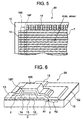
- FIG. 5 is a partially enlarged rear view of an organic EL display panel 30.
- This organic EL display panel 30 includes a plurality of organic EL elements D arranged in the form of a matrix on the substrate 10.
- the organic EL display panel 30 is constituted by sequentially laminating, on the substrate 10, row electrodes 13 having a transparent electrode layer (first display electrodes of the anode), an organic functional layer, and column electrodes 15 having a metal electrode layer (second display electrodes).
- the column electrodes 15 cross the row electrodes 13 at right angles.
- the row electrodes 13 are each formed having a belt (or band) shape and arranged in parallel at predetermined intervals from each other.
- the column electrodes 15 are each formed having a belt shape and arranged in parallel at predetermined intervals from each other.
- the matrix-display-type display panel 30 has an array of pixels. Specifically, a plurality of light emitting pixels (i.e., a plurality of organic EL elements) is formed at intersections of the row electrodes 13 and column electrodes 15 in the display panel 30.
- the organic EL display panel 30 may also include a plurality of partition walls 7 provided in parallel between the organic EL elements on the substrate 10.
- the high molecular compound film 16P is formed over the second display electrodes 15, the partition walls 7 and the peripheral area, so as to cover the organic EL elements completely. Once this high molecular compound film 16P has been made smooth, the inorganic barrier film 16S is formed thereon.
- the materials for the organic functional layer(s) may be selected and laminated to form red R, green G or blue B light emission portions.
- FIG. 6 shows an organic EL device 28 according to another embodiment of the present invention. Similar reference numerals and symbols are used to designate similar parts in Figures 1 and 6.
- This organic EL device 28 is the same as that of the embodiment shown in Figure 1 except for the fact that the substrate 10 is a plastic substrate consisting of a synthetic resin and the surface of the substrate 10 is covered with a barrier film 22 consisting of an inorganic material such as silicon nitride or silicon oxynitride (SiON).
- the first and second electrodes 13 and 15 of the organic EL element are formed on the inorganic barrier film 22.
- a film of polyethylene terephthalate, polyethylene-2,6-naphthalate, polycarbonate, polysulphone, polyethylsulphone, polyethylethylketone, polyphenoxyethyl, polyarylate, fluorine resin, polypropylene, or the like, can be used as the synthetic resin substrate 10.
- the surface of the plastic substrate 10 covered with the inorganic barrier film 22 preferably includes at least a surface that makes contact with the organic EL element D, a surface surrounding the organic EL element D, and a surface between the organic EL element D and an adjacent organic EL element (not shown).
- a surface on the rear side of the substrate 10 opposite the organic EL element D may also be covered with another barrier film (not shown).
- the barrier film(s) 22 prevent (s) penetration of outgas from the plastic substrate 10 to the organic functional layer 14. Further, warping of the plastic substrate 10 can be prevented by covering (sandwiching) both sides of the plastic substrate 10 with the inorganic barrier films 22.
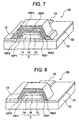
- Figure 7 shows an organic EL device 28 of another embodiment of the present invention. Similar reference numerals and symbols are used to designate similar parts in Figures 6 and 7.
- the organic EL element D is formed on the inorganic barrier film 22 of the substrate 10, and is protected by multiple-layer sealing part including the films 16S1, 16P1, 16S2, 16P2, 16S3 and 16P3.
- a first inorganic barrier film 1651 there are provided a first high molecular compound film 16P1, a second inorganic barrier film 16S2, a second high molecular compound film 16P2, a third inorganic barrier film 16S3, and a third high molecular compound film 16P3 in that order.
- the top surface of the second display electrode 15 is in contact with the first inorganic barrier film 16S1.
- the film deposition steps for the inorganic barrier film and high molecular compound film are alternately repeated. It should be noted that the lamination order of the inorganic barrier films 16S1 to 16S3 and high molecular compound films 16P1 to 16P3 may be reversed.
- the first high molecular compound film 16P1 may be formed on the top surface of the second display electrode 15, the first inorganic barrier film 16S1 may be formed on the first high molecular compound film 16P1, the second high molecular compound film 16P2 may be then formed on the first inorganic barrier film 16S1, and so on.
- a plastic substrate (10) having an inorganic barrier film (22) was prepared, and an organic functional layer (14) was formed on an anode (13) of the plastic substrate (10). Then, an Al cathode (15) was deposited on the organic functional layer (14) to create an organic EL element (D) on the substrate (10) .
- a polyurea high molecular compound film (16P1) was deposited by means of vapor deposition polymerization so as to cover the organic EL element (D), and a silicon nitride inorganic barrier film (16S1) was formed over the whole surface of the polyurea high molecular compound film (16P1) by means of plasma CVD.
- the edge (face) (E) of the high molecular compound film (16P1) and the peripheral substrate surface (R2) were also covered by the silicon nitride inorganic barrier film (16S1).
- the deposition processes for the polyurea high molecular compound film and silicon nitride inorganic barrier film were repeated to form a multilayered sealing (16P1, 16S1, 16P2, 16S2, 16P3 and 16S3) over the organic EL element (D).
- a multi-layer sealing part which is similar to Figure 7, was made over the organic EL element (D).
- an organic EL element sealed simply by a single-layer inorganic barrier film (22) was fabricated.
- the conditions for the plasma CVD of the silicon nitride film 10 SCCM silane (SiH 4 ) and 200 SCCM nitrogen gas were used, the pressure was 0.9 Torr, the RF power was 50 mW/cm 2 , the frequency was 13.56 MHz, the substrate temperature was 100°C, and the deposited film thickness was 1.0 ⁇ m.
- a test of the durability was conducted. In the atmosphere under the conditions of 60° C and 95% RH, the expansion of dark spots in these organic EL devices was measured. The test result revealed that there was no dark spot expansion in the organic EL device of this embodiment, but dark spot expansion occurred in the organic EL device of the comparative example.
- Figure 8 illustrates another embodiment of the present invention. Similar reference numerals and symbols are used to designate similar parts in Figures 7 and 8.
- the first inorganic barrier film 16S1 covers the organic EL element D and the peripheral substrate surface 10 (more specifically, the inorganic barrier film 22 formed on the substrate 10).
- the first high molecular compound film 16P1 covers the first inorganic barrier film 16S1 and the peripheral substrate surface 10.
- the second inorganic barrier film 16S2 covers the first high molecular compound film 16P1, the edge face (lateral face) thereof, and the peripheral substrate surface.
- the second high molecular compound film 16P2 covers the second inorganic barrier film 16S2, the edge face thereof, and the peripheral substrate surface.
- Masks having different sizes of opening are used to deposit the films 16S1, 16P1, 16S2 and 16P2 such that the respective openings of the masks allow the passage of respective deposition materials.
- the opening of one mask has a larger size than the opening of another mask used in the preceding step.
- the multi-layer protective part including the films 16S1, 16P1, 16S2 and 16P2, can be deposited in a desired manner.
- One film covers the edge face of the preceding film in the multi-layer part.
- the inside high molecular compound film (16P1; 16P2) is sandwiched and embedded between a pair of inorganic barrier films (16S1 and 16S2; 16S2 and 16S3).
- the inorganic barrier films 22 and 16S1 are always in contact with the organic EL element D. It can be said that the inorganic barrier film 16S1 is always in contact with the organic EL element D.
- a multilayered sealing part in which at least one inorganic barrier film and at least one high molecular compound film are laminated, is provided over the organic EL element D. Therefore, pinholes that may be present in the inorganic barrier film are embedded in and rendered smooth by the high molecular compound film. Thus, the multilayered sealing part does not include defects. Further, the second (and third) inorganic barrier film is laminated over the high molecular compound film(s) in the embodiments of Figures 7 and 8. Thus, the sealing effect of the multilayered sealing part is further enhanced in these embodiments.
- vapor deposition polymerization is employed in the above embodiments as the method for fabricating a high molecular compound film of polyureas or the like, the present invention is not restricted to this method. Chemical vapor deposition, vacuum spraying, and so-called sputtering can also be applied.
- Vacuum spraying involves the deposition of a film by spraying a polymer solution via a nozzle in a vacuum or inert gas.
- the solvent becomes volatile immediately and disappears before reaching the substrate. If the substrate is heated to a temperature (about 100° C) of a magnitude so as not to damage the organic functional layer of the organic EL element, the solvent becomes volatile even if the solvent remains in the film.
- a solvent is preferably selected to have a volatility temperature lower than the temperature of the substrate heated, so that the solvent becomes volatile at the same time as the solution adheres to the substrate, and hence solvent that would otherwise damage the organic EL element no longer remains.
- a vacuum spraying device includes a vacuum chamber, a fluid spraying device connected to the vacuum chamber, an exhaust system connected to the vacuum chamber, and a substrate heating holder located in the vacuum chamber.
- the present invention can also be applied to the substrate of an active matrix display type panel using a TFT and so forth.
Landscapes
- Chemical & Material Sciences (AREA)
- Inorganic Chemistry (AREA)
- Physics & Mathematics (AREA)
- Optics & Photonics (AREA)
- Electroluminescent Light Sources (AREA)
- Physical Vapour Deposition (AREA)
Applications Claiming Priority (2)
| Application Number | Priority Date | Filing Date | Title |
|---|---|---|---|
| JP2003071423 | 2003-03-17 | ||
| JP2003071423A JP2004281247A (ja) | 2003-03-17 | 2003-03-17 | 有機エレクトロルミネッセンス表示パネル及びその製造方法 |
Publications (2)
| Publication Number | Publication Date |
|---|---|
| EP1460697A2 true EP1460697A2 (de) | 2004-09-22 |
| EP1460697A3 EP1460697A3 (de) | 2006-05-10 |
Family
ID=32821276
Family Applications (1)
| Application Number | Title | Priority Date | Filing Date |
|---|---|---|---|
| EP04251435A Withdrawn EP1460697A3 (de) | 2003-03-17 | 2004-03-12 | Organische elektrolumineszente Anzeigevorrichtung und Herstellungsverfahren |
Country Status (4)
| Country | Link |
|---|---|
| US (2) | US20040232832A1 (de) |
| EP (1) | EP1460697A3 (de) |
| JP (1) | JP2004281247A (de) |
| CN (1) | CN1531381A (de) |
Cited By (4)
| Publication number | Priority date | Publication date | Assignee | Title |
|---|---|---|---|---|
| WO2007043703A1 (en) * | 2005-10-14 | 2007-04-19 | Matsushita Electric Industrial Co., Ltd. | Light emitting apparatus, exposure apparatus, and method for manufacturing light emitting apparatus |
| EP1916725A1 (de) * | 2006-10-27 | 2008-04-30 | Nederlandse Organisatie voor toegepast-natuurwetenschappelijk Onderzoek TNO | Vorrichtung mit organichen lichtemittierenden Dioden und mehrschichtiger Abdichtung |
| EP2135971A4 (de) * | 2007-04-16 | 2012-08-08 | Ulvac Inc | Polyharnstofffilm und verfahren zu seiner herstellung |
| EP3163646A1 (de) * | 2015-10-29 | 2017-05-03 | LG Display Co., Ltd. | Organische lichtemittierende anzeigevorrichtung |
Families Citing this family (37)
| Publication number | Priority date | Publication date | Assignee | Title |
|---|---|---|---|---|
| JP4643138B2 (ja) * | 2003-11-27 | 2011-03-02 | 東芝モバイルディスプレイ株式会社 | 表示装置及びその製造方法 |
| TWI367686B (en) * | 2004-04-07 | 2012-07-01 | Semiconductor Energy Lab | Light emitting device, electronic device, and television device |
| US20060066235A1 (en) * | 2004-09-27 | 2006-03-30 | Brody Thomas P | Receptacles for inkjet deposited PLED/OLED devices and method of making the same |
| JP4887473B2 (ja) * | 2005-06-30 | 2012-02-29 | エルジー ディスプレイ カンパニー リミテッド | 有機el素子及びそれを用いた有機elディスプレイ並びに有機elディスプレイの製造方法 |
| JP4795779B2 (ja) * | 2005-11-09 | 2011-10-19 | 株式会社アルバック | 有機エレクトロルミネッセンス表示パネル |
| JP2007134243A (ja) * | 2005-11-11 | 2007-05-31 | Sony Corp | 表示装置の製造方法およびマスク |
| JP4702009B2 (ja) | 2005-11-22 | 2011-06-15 | セイコーエプソン株式会社 | 発光装置および電子機器 |
| JP5268249B2 (ja) * | 2005-12-14 | 2013-08-21 | キヤノン株式会社 | 有機発光素子の製造方法 |
| US20070164673A1 (en) * | 2006-01-18 | 2007-07-19 | Au Optronics Corporation | Organic electro-luminescent display device and method for making same |
| JPWO2007123102A1 (ja) * | 2006-04-18 | 2009-09-03 | 株式会社アルバック | 成膜装置、バリア膜製造方法 |
| TWI307611B (en) * | 2006-06-05 | 2009-03-11 | Au Optronics Corp | Organic electroluminescence device and organic electroluminescence panel using the same |
| US20080138624A1 (en) * | 2006-12-06 | 2008-06-12 | General Electric Company | Barrier layer, composite article comprising the same, electroactive device, and method |
| US20080138538A1 (en) * | 2006-12-06 | 2008-06-12 | General Electric Company | Barrier layer, composite article comprising the same, electroactive device, and method |
| KR101369910B1 (ko) * | 2007-03-30 | 2014-03-05 | 삼성전자주식회사 | 유기전계 발광소자 및 그 제조방법 |
| US7795613B2 (en) * | 2007-04-17 | 2010-09-14 | Toppan Printing Co., Ltd. | Structure with transistor |
| KR100943185B1 (ko) * | 2008-04-24 | 2010-02-19 | 삼성모바일디스플레이주식회사 | 유기 발광 디스플레이 장치 |
| US8053984B2 (en) * | 2008-05-26 | 2011-11-08 | Lg Display Co., Ltd. | Organic light emitting diode display |
| CN101436648B (zh) * | 2008-12-09 | 2010-06-16 | 彩虹集团公司 | 一种新型有机电致发光器件薄膜封装方法 |
| EP2273579A1 (de) * | 2009-07-10 | 2011-01-12 | Nederlandse Organisatie voor toegepast -natuurwetenschappelijk onderzoek TNO | Verfahren zur Verkapselung einer flexiblen optoelektronischen mehrschichtigen Struktur |
| KR101097321B1 (ko) * | 2009-12-14 | 2011-12-23 | 삼성모바일디스플레이주식회사 | 유기 발광 장치 및 이의 제조 방법 |
| KR20120065049A (ko) * | 2010-12-10 | 2012-06-20 | 삼성모바일디스플레이주식회사 | 유기발광 표시장치 및 그 제조 방법 |
| JP2012209209A (ja) * | 2011-03-30 | 2012-10-25 | Toppan Printing Co Ltd | 有機エレクトロルミネッセンスパネルの製造方法 |
| KR101863853B1 (ko) * | 2011-07-29 | 2018-06-04 | 삼성디스플레이 주식회사 | 유기 발광 표시장치 및 그 제조방법 |
| WO2013027278A1 (ja) * | 2011-08-24 | 2013-02-28 | パイオニア株式会社 | 有機発光パネル及びその製造方法 |
| KR20140066974A (ko) | 2011-09-26 | 2014-06-03 | 파나소닉 주식회사 | 발광 장치의 제조 방법 및 발광 장치 |
| US9853245B2 (en) | 2011-10-14 | 2017-12-26 | Samsung Display Co., Ltd. | Organic light emitting diode display and method for manufacturing the same |
| JP6054763B2 (ja) | 2013-02-12 | 2016-12-27 | 株式会社ジャパンディスプレイ | 有機el表示装置 |
| KR20150011231A (ko) * | 2013-07-22 | 2015-01-30 | 삼성디스플레이 주식회사 | 유기 발광 표시 장치 및 이의 제조 방법 |
| WO2015029608A1 (ja) * | 2013-08-28 | 2015-03-05 | シャープ株式会社 | エレクトロルミネッセンス装置、及びその製造方法 |
| JP6254459B2 (ja) * | 2014-02-27 | 2017-12-27 | 東京エレクトロン株式会社 | 重合膜の耐薬品性改善方法、重合膜の成膜方法、成膜装置、および電子製品の製造方法 |
| KR102253531B1 (ko) | 2014-07-25 | 2021-05-18 | 삼성디스플레이 주식회사 | 표시 장치 및 그 제조 방법 |
| CN104659271B (zh) * | 2015-03-17 | 2017-03-01 | 京东方科技集团股份有限公司 | 一种有机发光二极管封装结构及封装方法、显示装置 |
| JP6584162B2 (ja) * | 2015-06-22 | 2019-10-02 | 東京エレクトロン株式会社 | 積層封止膜形成方法および形成装置 |
| JP2017152256A (ja) * | 2016-02-25 | 2017-08-31 | 株式会社ジャパンディスプレイ | 表示装置 |
| CN114899346B (zh) * | 2017-06-13 | 2025-07-29 | 堺显示器制品株式会社 | 有机el设备的制造方法及薄膜密封结构形成装置 |
| KR102814722B1 (ko) * | 2019-10-29 | 2025-05-30 | 삼성디스플레이 주식회사 | 디스플레이 장치 |
| KR102775872B1 (ko) * | 2020-04-09 | 2025-03-05 | 삼성디스플레이 주식회사 | 표시 장치 및 그 제조 방법 |
Family Cites Families (19)
| Publication number | Priority date | Publication date | Assignee | Title |
|---|---|---|---|---|
| JPS6441192A (en) * | 1987-08-07 | 1989-02-13 | Alps Electric Co Ltd | Thin film electroluminescent display element |
| JP2774351B2 (ja) * | 1990-03-26 | 1998-07-09 | 出光興産株式会社 | 有機薄膜エレクトロルミネッセンス素子及びその製造方法 |
| JP3101300B2 (ja) * | 1990-07-13 | 2000-10-23 | 三洋電機株式会社 | 有機電界発光素子 |
| EP0566736B1 (de) * | 1990-11-30 | 1998-07-29 | Idemitsu Kosan Company Limited | Organische elektroluminszente vorrichtung |
| JPH07169569A (ja) * | 1993-12-17 | 1995-07-04 | Idemitsu Kosan Co Ltd | 有機el素子およびその製造方法 |
| JP3615817B2 (ja) * | 1995-02-14 | 2005-02-02 | 株式会社アルバック | 有機エレクトロルミネッセンス素子の製造方法 |
| JP3162313B2 (ja) * | 1997-01-20 | 2001-04-25 | 工業技術院長 | 薄膜製造方法および薄膜製造装置 |
| JPH10247587A (ja) * | 1997-02-28 | 1998-09-14 | Tdk Corp | 有機エレクトロルミネッセンス表示装置およびその製造方法 |
| JP3199006B2 (ja) * | 1997-11-18 | 2001-08-13 | 日本電気株式会社 | 層間絶縁膜の形成方法および絶縁膜形成装置 |
| JP4040240B2 (ja) * | 2000-07-10 | 2008-01-30 | パナソニック コミュニケーションズ株式会社 | 有機エレクトロルミネッセンス素子及びその製造方法 |
| TWI226205B (en) * | 2000-03-27 | 2005-01-01 | Semiconductor Energy Lab | Self-light emitting device and method of manufacturing the same |
| JP4004709B2 (ja) * | 2000-03-30 | 2007-11-07 | パイオニア株式会社 | 有機エレクトロルミネッセンス表示パネル及びその製造方法 |
| JP2001307873A (ja) * | 2000-04-21 | 2001-11-02 | Toppan Printing Co Ltd | 有機エレクトロルミネッセンス表示素子およびその製造方法 |
| JP3783099B2 (ja) * | 2000-05-16 | 2006-06-07 | 株式会社豊田中央研究所 | 有機電界発光素子 |
| JP2002100469A (ja) * | 2000-09-25 | 2002-04-05 | Pioneer Electronic Corp | 有機エレクトロルミネッセンス表示パネル |
| US6664137B2 (en) * | 2001-03-29 | 2003-12-16 | Universal Display Corporation | Methods and structures for reducing lateral diffusion through cooperative barrier layers |
| TW490868B (en) * | 2001-08-10 | 2002-06-11 | Ritdisplay Corp | Method for forming a waterproof layer of organic light emitting device |
| JP2003282241A (ja) * | 2002-03-25 | 2003-10-03 | Pioneer Electronic Corp | 有機エレクトロルミネッセンス表示パネル及び製造方法 |
| JP2004103442A (ja) * | 2002-09-11 | 2004-04-02 | Ulvac Japan Ltd | 有機el素子及びその製造方法 |
-
2003
- 2003-03-17 JP JP2003071423A patent/JP2004281247A/ja active Pending
-
2004
- 2004-03-11 US US10/797,573 patent/US20040232832A1/en not_active Abandoned
- 2004-03-12 EP EP04251435A patent/EP1460697A3/de not_active Withdrawn
- 2004-03-17 CN CNA2004100294054A patent/CN1531381A/zh active Pending
-
2006
- 2006-08-04 US US11/498,769 patent/US20060275540A1/en not_active Abandoned
Non-Patent Citations (1)
| Title |
|---|
| ATSUSHI KUBONO ET AL: "DIRECT FORMATION OF POLYMIDE THIN FILMS BY VAPOR DEPOSITION POLYMERIZATION", THIN SOLID FILMS, ELSEVIER-SEQUOIA S.A. LAUSANNE, CH LNKD- DOI:10.1016/0040-6090(93)90018-K, vol. 232, no. 2, 2 September 1993 (1993-09-02), pages 256 - 260, XP000396068, ISSN: 0040-6090 * |
Cited By (7)
| Publication number | Priority date | Publication date | Assignee | Title |
|---|---|---|---|---|
| WO2007043703A1 (en) * | 2005-10-14 | 2007-04-19 | Matsushita Electric Industrial Co., Ltd. | Light emitting apparatus, exposure apparatus, and method for manufacturing light emitting apparatus |
| EP1916725A1 (de) * | 2006-10-27 | 2008-04-30 | Nederlandse Organisatie voor toegepast-natuurwetenschappelijk Onderzoek TNO | Vorrichtung mit organichen lichtemittierenden Dioden und mehrschichtiger Abdichtung |
| WO2008051078A3 (en) * | 2006-10-27 | 2008-06-26 | Tno | Organic light emitting diode device with multilayer seal |
| EP2135971A4 (de) * | 2007-04-16 | 2012-08-08 | Ulvac Inc | Polyharnstofffilm und verfahren zu seiner herstellung |
| KR101443941B1 (ko) * | 2007-04-16 | 2014-09-23 | 가부시키가이샤 알박 | 폴리우레아막 및 그 성막 방법 |
| EP3163646A1 (de) * | 2015-10-29 | 2017-05-03 | LG Display Co., Ltd. | Organische lichtemittierende anzeigevorrichtung |
| US10326110B2 (en) | 2015-10-29 | 2019-06-18 | Lg Display Co., Ltd. | Organic light emitting display device |
Also Published As
| Publication number | Publication date |
|---|---|
| JP2004281247A (ja) | 2004-10-07 |
| US20040232832A1 (en) | 2004-11-25 |
| CN1531381A (zh) | 2004-09-22 |
| US20060275540A1 (en) | 2006-12-07 |
| EP1460697A3 (de) | 2006-05-10 |
Similar Documents
| Publication | Publication Date | Title |
|---|---|---|
| EP1460697A2 (de) | Organische elektrolumineszente Anzeigevorrichtung und Herstellungsverfahren | |
| US7102176B2 (en) | Organic electroluminescent display panel and manufacturing method therefor | |
| US7208872B2 (en) | Multilayer barrier film structure and organic electroluminescent display panel and manufacturing method thereof | |
| KR101303291B1 (ko) | 발광장치 제작방법 및 증착장치 | |
| KR101481749B1 (ko) | 제조 시스템 | |
| JP3783099B2 (ja) | 有機電界発光素子 | |
| US20050023974A1 (en) | Protected organic electronic devices and methods for making the same | |
| US20100244068A1 (en) | Method For Applying A Thin-Film Encapsulation Layer Assembly To An Organic Device, And An Organic Device Provided With A Thin-Film Encapsulation Layer Assembly Preferably Applied With Such A Method | |
| US20050174045A1 (en) | Organic light-emitting device display having a plurality of passive polymer layers | |
| US20070184292A1 (en) | Flat panel display device and manufacturing method for the same | |
| CN100459209C (zh) | 有机电致发光面板及其制造方法 | |
| JP2003017244A (ja) | 有機電界発光素子およびその製造方法 | |
| CN1239395A (zh) | 制造有机场致发光显示板的方法 | |
| KR20040014659A (ko) | 유기 광발산 장치용 투명 지지체 | |
| KR20110068176A (ko) | 플렉서블 디스플레이용 기판, 이를 제조하는 방법, 및 이 기판제조방법을 이용한 유기 발광 디스플레이 장치의 제조 방법 | |
| KR20050112318A (ko) | 평판 표시장치의 제조방법, 평판 표시장치, 및 평판표시장치의 패널 | |
| US7696683B2 (en) | Organic electroluminescent element and the manufacturing method | |
| WO2007055168A1 (ja) | 有機エレクトロルミネッセンス表示パネル | |
| US7549905B2 (en) | Method of encapsulating an organic light emitting device | |
| US20050168136A1 (en) | Organic electroluminescence display panel and method for manufacturing the same | |
| JP2004103442A (ja) | 有機el素子及びその製造方法 | |
| US20050158454A1 (en) | Method and system for forming an organic light-emitting device display having a plurality of passive polymer layers | |
| JP2007059407A (ja) | 有機電界発光表示装置およびこれに備えられる有機薄膜トランジスタ | |
| KR101369908B1 (ko) | 유기 전계 발광 소자 및 그 제조 방법 | |
| KR100592280B1 (ko) | 평판 표시장치의 제조방법, 및 평판 표시장치 |
Legal Events
| Date | Code | Title | Description |
|---|---|---|---|
| PUAI | Public reference made under article 153(3) epc to a published international application that has entered the european phase |
Free format text: ORIGINAL CODE: 0009012 |
|
| 17P | Request for examination filed |
Effective date: 20040330 |
|
| AK | Designated contracting states |
Kind code of ref document: A2 Designated state(s): AT BE BG CH CY CZ DE DK EE ES FI FR GB GR HU IE IT LI LU MC NL PL PT RO SE SI SK TR |
|
| AX | Request for extension of the european patent |
Extension state: AL HR LT LV MK |
|
| PUAL | Search report despatched |
Free format text: ORIGINAL CODE: 0009013 |
|
| AK | Designated contracting states |
Kind code of ref document: A3 Designated state(s): AT BE BG CH CY CZ DE DK EE ES FI FR GB GR HU IE IT LI LU MC NL PL PT RO SE SI SK TR |
|
| AX | Request for extension of the european patent |
Extension state: AL LT LV MK |
|
| AKX | Designation fees paid |
Designated state(s): DE FR GB |
|
| 17Q | First examination report despatched |
Effective date: 20061221 |
|
| RAP1 | Party data changed (applicant data changed or rights of an application transferred) |
Owner name: PIONEER CORPORATION |
|
| STAA | Information on the status of an ep patent application or granted ep patent |
Free format text: STATUS: THE APPLICATION IS DEEMED TO BE WITHDRAWN |
|
| 18D | Application deemed to be withdrawn |
Effective date: 20101110 |