EP1460711A1 - Elektronisches Chip-Bauteil - Google Patents
Elektronisches Chip-Bauteil Download PDFInfo
- Publication number
- EP1460711A1 EP1460711A1 EP04004025A EP04004025A EP1460711A1 EP 1460711 A1 EP1460711 A1 EP 1460711A1 EP 04004025 A EP04004025 A EP 04004025A EP 04004025 A EP04004025 A EP 04004025A EP 1460711 A1 EP1460711 A1 EP 1460711A1
- Authority
- EP
- European Patent Office
- Prior art keywords
- electrode
- chip
- ground
- electrodes
- ground electrode
- Prior art date
- Legal status (The legal status is an assumption and is not a legal conclusion. Google has not performed a legal analysis and makes no representation as to the accuracy of the status listed.)
- Granted
Links
- 230000008878 coupling Effects 0.000 claims description 4
- 238000010168 coupling process Methods 0.000 claims description 4
- 238000005859 coupling reaction Methods 0.000 claims description 4
- 239000000758 substrate Substances 0.000 description 13
- 230000005540 biological transmission Effects 0.000 description 6
- 230000000052 comparative effect Effects 0.000 description 5
- 230000002349 favourable effect Effects 0.000 description 5
- 238000012986 modification Methods 0.000 description 2
- 230000004048 modification Effects 0.000 description 2
- 239000000919 ceramic Substances 0.000 description 1
- 229910010293 ceramic material Inorganic materials 0.000 description 1
- 230000007423 decrease Effects 0.000 description 1
- 239000003989 dielectric material Substances 0.000 description 1
- 230000000694 effects Effects 0.000 description 1
- 230000005684 electric field Effects 0.000 description 1
- 238000005516 engineering process Methods 0.000 description 1
- 229920002313 fluoropolymer Polymers 0.000 description 1
- 238000010030 laminating Methods 0.000 description 1
- 238000003475 lamination Methods 0.000 description 1
- 238000004806 packaging method and process Methods 0.000 description 1
Images




Classifications
-
- H—ELECTRICITY
- H01—ELECTRIC ELEMENTS
- H01P—WAVEGUIDES; RESONATORS, LINES, OR OTHER DEVICES OF THE WAVEGUIDE TYPE
- H01P7/00—Resonators of the waveguide type
- H01P7/08—Strip line resonators
-
- H—ELECTRICITY
- H01—ELECTRIC ELEMENTS
- H01P—WAVEGUIDES; RESONATORS, LINES, OR OTHER DEVICES OF THE WAVEGUIDE TYPE
- H01P7/00—Resonators of the waveguide type
- H01P7/08—Strip line resonators
- H01P7/082—Microstripline resonators
-
- H—ELECTRICITY
- H01—ELECTRIC ELEMENTS
- H01P—WAVEGUIDES; RESONATORS, LINES, OR OTHER DEVICES OF THE WAVEGUIDE TYPE
- H01P7/00—Resonators of the waveguide type
- H01P7/08—Strip line resonators
- H01P7/084—Triplate line resonators
Definitions
- the present invention relates to electronic chip components used as chip resonant elements and band-pass filters. More specifically, the present invention relates to a electronic chip component including a chip provided with a resonator electrode and input and output electrodes connected or coupled to the resonator electrode.
- band-pass filters used in high-frequency regions, such as dual-mode band-pass filters and band-pass filters using a wavelength resonator, have been proposed.
- Patent Document 1 Japanese Unexamined Patent Application Publication No. 2001-237610, discloses a dual-mode band-pass filter using a resonator electrode including a through hole.
- a dual-mode band-pass filter 101 includes a dielectric substrate 102.
- a resonator electrode 103 is disposed at the center in a height direction of the dielectric substrate 102.
- the resonator electrode 103 includes a through hole 103a.
- the resonator electrode 103 generates a plurality of resonance modes which are not degraded.
- the through hole 103a couples the resonance modes, such that the dual-mode band-pass filter is obtained.
- Ground electrodes 104 and 105 which face the resonator electrode 103, are disposed on the upper and lower surfaces of the dielectric substrate 102. Also, as shown in Fig. 15B, input/output coupled electrodes 106 and 107 are coupled to the resonator electrode 103. Although not shown in Fig. 15A, the input/output coupled electrodes 106 and 107 extend outward from the vicinity of the resonator electrode 103 and are electrically connected to input/output electrodes (not shown).
- the ground electrode In a chip-shaped band-pass filter in which ground electrodes are disposed over and under a resonator electrode via dielectric substrate layers, such as the dual-mode band-pass filter 101, or in a band-pass filter in which a ground electrode covers four surfaces of a substrate, the ground electrode is usually also provided on side surfaces of the dielectric substrate. Therefore, the ground electrodes define a waveguide. In other words, the resonator electrode 103 is in the waveguide. With this configuration, resonance is generated depending only on the shape of the waveguide. On the other hand, the above-described waveguide portion defined by the ground electrodes is inevitably larger than the resonator electrode 103.
- a basic-mode resonance caused by the ground electrodes is generated at the side of a frequency lower than the resonance frequency of the resonator electrode 103, and higher modes thereof tend to be generated one after another at the portion overlapping the resonance mode of the resonator electrode 103.
- the resonance caused by the ground electrodes generates undesired spurious signals in the dual-mode band-pass filter 101, and thus a favorable transmission characteristic is not obtained.
- preferred embodiments of the present invention provide a band-pass filter that suppresses undesired spurious signals based on resonance caused by a ground electrode and that has a favorable transmission characteristic.
- the electronic chip component includes a chip having upper and lower surfaces, a pair of side surfaces, and first and second end surfaces facing each other, a resonator electrode in the chip, input and output electrodes extending in the vertical direction, which are coupled or connected to the resonator electrode, and a first ground electrode around the chip, the first ground electrode having a tubular shape so as to enclose the resonator electrode.
- the input and output electrodes are disposed at end portions or inner sides of the tubular first ground electrode, such that the input and output electrodes are not electrically connected to the first ground electrode.
- the electronic chip component further includes at least a pair of second ground electrodes which are disposed on both sides of the input electrode and/or the output electrode and which are electrically connected to the first ground electrode.
- the chip is preferably substantially rectangular, the input and output electrodes are preferably disposed on the first and second end surfaces facing each other, respectively, and the first ground electrode preferably includes surfaces that are substantially parallel with the upper and lower surfaces and the pair of side surfaces of the chip so as to have a tubular shape.
- At least one of the surfaces of the first ground electrode that is substantially parallel with the upper and lower surfaces and the pair of side surfaces of the chip may is preferably embedded in the chip.
- the first ground electrode preferably surrounds the upper and lower surfaces and the pair of side surfaces of the chip. In that case, the first ground electrode is easily formed by providing a conductive film on the outer surface of the chip.
- the input and output electrodes may extend in the vertical direction on the first and second end surfaces, respectively. In that case, the input and output electrodes can be easily formed by applying conductive films on the end surfaces.
- the input and output electrodes preferably include via-hole electrodes which extend in the vertical direction in the chip and which are led to the upper or lower surface of the chip so as not to be electrically connected to the first ground electrode. In that case, the entire outer surface of the chip except a region to which the input and output electrodes are led is covered by the first ground electrode, so as to enhance an electromagnetic shielding characteristic. Also, packaging space in the electronic chip component is saved.
- the second ground electrodes preferably extend in the vertical direction at the end surfaces of the chip. In that case, the portion of the second ground electrodes on the end surfaces of the chip is easily formed by applying conductive films on the end surfaces.
- the second ground electrodes preferably extend in the vertical direction in the chip and are electrically connected to the first ground electrode at the upper surface and/or the lower surface of the chip.
- the second ground electrodes are formed by using via-hole electrodes. Therefore, the positions of the second ground electrodes are precisely adjusted so as to suppress undesired spurious signals more effectively.
- the resonator electrode is preferably configured so as to generate a plurality of resonance modes which are not degraded and the resonator electrode preferably includes a through hole for coupling the plurality of resonance modes, whereby a band-pass filter is obtained.
- a band-pass filter having a favorable transmission characteristic is obtained according to preferred embodiments of the present invention.
- the electronic chip component preferably further includes a third ground electrode which extends in the through hole so as not to be in contact with the resonator electrode and which is electrically connected to the first ground electrode.
- the third ground electrode further suppresses undesired spurious signals.
- the resonator electrode may be a ring-shaped resonator.
- a dual-mode band-pass filter generating reduced undesired spurious signals is provided according to preferred embodiments of the present invention.
- FIGs. 1A and 1 B are a perspective view and a plan view showing a band-pass filter 1 serving as a electronic chip component according to a first preferred embodiment of the present invention.
- the band-pass filter 1 includes a substantially rectangular chip 2.
- the chip 2 includes a dielectric substrate, which includes an adequate dielectric material, such as fluoroplastics or ceramic.
- a resonator electrode 3 is disposed at the approximate center in a height direction of the chip 2. Further, as shown in the schematic cross-sectional view in Fig. 3 taken along the horizontal plane, the resonator electrode 3 includes a metallic film having a through hole 3a. The resonator electrode 3 generates two resonance modes which are not degraded. The two resonance modes are coupled by the through hole 3a, such that a band-pass filter is obtained.
- the coupling degree of the two resonance modes is freely and significantly adjusted by adjusting the size of the through hole 3a.
- Such a band-pass filter is disclosed in the above-described Patent Document 1.
- input/output coupled electrodes 4 and 5 are disposed at a different height from the resonator electrode 3 so as to have lamination capacitance with the resonator electrode 3.
- the input/output coupled electrodes 4 and 5 are led to a pair of end surfaces 2a and 2b facing each other of the chip 2, respectively.
- the chip 2 includes the end surfaces 2a and 2b, an upper surface 2c, a lower surface 2d, and side surfaces 2e and 2f.
- the chip 2 is formed by laminating a plurality of dielectric layers.
- Each of the resonator electrode 3, the input/output coupled electrodes 4 and 5, and a first ground electrode 10 is provided on an upper or lower surface of one of the dielectric layers.
- the input/output coupled electrodes 4 and 5 may be disposed at the same position as the resonator electrode 3 in a height direction, such that the input/output coupled electrodes 4 and 5 are separated from the resonator electrode 3.
- An input electrode 6 and an output electrode 7 are disposed on the end surfaces 2a and 2b, respectively.
- the input and output electrodes 6 and 7 are electrically connected to the input/output coupled electrodes 4 and 5, respectively.
- the input and output electrodes 6 and 7 extend in the vertical direction on the end surfaces 2a and 2b.
- the first ground electrode 10 is disposed around the outer surface of the chip 2.
- the first ground electrode 10 covers the upper and lower surfaces 2c and 2b and the side surfaces 2e and 2f of the chip 2.
- the first ground electrode 10 includes notches 10a and 10b at the upper surface 2c so as to prevent short circuit caused between the first ground electrode 10 and the input and output electrodes 6 and 7.
- notches are provided in the first ground electrode 10 at the lower surface 2d of the chip 2.
- the first ground electrode 10 covers the upper and lower surfaces 2c and 2d and the side surfaces 2e and 2f of the chip 2, except the notches 10a and 10b and the notches provided at the lower surface.
- the first ground electrode 10 has a tubular shape.
- the band-pass filter 1 of this preferred embodiment includes a pair of second ground electrodes 11 and 12 are disposed on both sides of the input electrode 6, and a pair of second ground electrodes 13 and 14 are disposed on both sides of the output electrode 7.
- each of the second ground electrodes 11 to 14 includes a via-hole electrode for connecting upper and lower portions of the first ground electrode 10 on the upper and lower surfaces 2c and 2d of the chip 2. That is, the upper and lower portions of the first ground electrode 10 around the chip 2 are electrically connected by the second ground electrodes 11 to 14.
- the via-hole electrodes in the chip 2 function as the second ground electrodes 11 to 14, which are positioned at the inner sides of the ends of the tubular first ground electrode 10 but at the closest positions to the input and output electrodes 6 and 7.
- the electric field is controlled by providing the second ground electrodes 11 to 14, which suppresses the undesired spurious signals. This will be described below based on a specific example.
- a chip component which is the same as the band-pass filter 1 except that the resonator electrode 3 and the input/output coupled electrodes 4 and 5 are not provided was prepared.
- a substantially rectangular dielectric substrate which includes a ceramic material primarily containing an oxide such as Ba, Al, and Si and which has a size of, for example, about 3.2 x about 4.5 x about 0.5 (thickness) mm was used.
- the input and output electrodes 6 and 7 having a width of about 0.4 mm were provided at the approximate center of the end surfaces 2a and 2b of the chip 2 in the vertical direction, respectively.
- the notches 10a and 10b on the upper surface and the notches on the lower surface were provided in a size of about 0.5 mm ⁇ about 0.5 mm in the width and longitudinal directions of the chip 2.
- the second ground electrodes 11 to 14 were positioned about 0.35 mm inside the end surfaces 2a and 2b of the chip 2. Also, each of the second ground electrodes 11 to 14 was positioned at a distance of x mm in the width direction of the chip 2 from the center in the width direction of the chip 2, that is, the center in the width direction of the input electrode 6 or the output electrode 7.
- the distance x was varied in the range of about 0.4 mm, about 0.5 mm, about 0.55 mm, and about 0.6 mm, so as to prepare four types of chip components, and the frequency characteristics of each component were obtained. The result is shown in Figs. 4 and 5.
- Fig. 4 shows the frequency characteristics of each of the prepared chip components
- Fig. 5 is an enlarged view showing the critical portion of the characteristics shown in Fig. 4.
- the relative permittivity ⁇ r was set to about 6.27 and tan ⁇ was set to about 0.001 in the chip 2
- each of the resonator electrode 3, input and output electrodes 6 and 7, first ground electrode 10, and second ground electrodes 11 to 14 were formed by using Cu.
- a curve Pa-1 in Figs. 4 and 5 indicates the frequency characteristics of the chip component prepared for comparison.
- Curves Pa-2 to Pa-5 indicate the frequency characteristics of resonance of the chip components in which the distance x is about 0.4 mm, about 0.5 mm, about 0.55 mm, or about 0.6 mm.
- spurious signals S1 and S2 of attenuation of about 5 dB or less is generated at about 20.4 GHz and about 24.4 GHz. Also, shown in the figure, a frequency band in which the attenuation level is about 15 dB or less does not exist in the range of about 20 GHz to about 30 GHz.
- spurious signals caused at about 20.4 GHz and about 24.4 GHz are suppressed in the chip components 1 including the second ground electrodes 11 to 14. Also, although spurious signal is generated at the vicinity of about 25 GHz, attenuation in the other region of the about 20 GHz to about 30 GHz band is reduced to about 20 dB or less.
- the input electrode 6 or the output electrode 7 and the second ground electrodes 11 to 14 may not be provided on the same plane or in a line.
- the input/output coupled electrodes 4 and 5 may be extended between the pair of second ground electrodes 11 and 12 and between 13 and 14, which connect the upper and lower portions of the first ground electrode 10. Accordingly, freedom of design is enhanced.
- the chip components including the second ground electrodes 11 to 14 have a more enhanced transmission characteristic than that of the chip component of the comparative example which does not include the second ground electrodes 11 to 14.
- the resonator electrode 3 prepared by forming a through hole 3a having a size of about 0.9 mm ⁇ about 0.8 mm in a circular metallic film having a radius of about 1.1 mm and the input/output coupled electrodes 4 and 5 were further provided in the chip component including the second ground electrodes 11 to 14, so as to produce the band-pass filter 1 according to the first preferred embodiment.
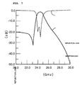
- Fig. 7 shows an example of the frequency characteristic of the dual-mode band-pass filter 1 formed in the above-described manner. As can be seen, spurious signals do not appear in Fig. 7.
- spurious signals caused by the shape of filter that is, spurious signals caused by the ground electrode in a shape of a waveguide, are suppressed, and the band-pass filter is obtained.
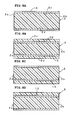
- Figs. 8A to 8D are schematic cross-sectional views showing modifications of the band-pass filter 1 of this preferred embodiment.
- the first ground electrode 10 covers the upper and lower surfaces of the chip 2. That is, as shown in Fig. 8A, the first ground electrode 10 is disposed on the upper and lower surfaces 2c and 2d of the chip 2.
- a portion of the first ground electrode 10 which is substantially parallel to the upper or lower surface of the chip 2 may be embedded in the chip 2.
- both upper and lower portions of the first ground electrode 10 which are substantially parallel to the upper and lower surfaces 2c and 2d are embedded in the chip 2.
- Fig. 8B both upper and lower portions of the first ground electrode 10 which are substantially parallel to the upper and lower surfaces 2c and 2d are embedded in the chip 2.
- the portion of the first ground electrode 10 that is substantially parallel to the lower surface 2d is embedded in the chip 2, and the portion that is substantially parallel to the upper surface 2c is disposed on the upper surface 2c.
- the portion of the first ground electrode that is substantially parallel to the upper surface 2c is embedded in the chip 2, and the portion that is substantially parallel to the lower surface 2d is disposed on the lower surface 2d.
- the portions of the first ground electrode 10 that are substantially parallel to the side surfaces 2e and 2f may be embedded in the chip 2.
- Fig. 9 is a schematic cross-sectional view illustrating the shape of a resonator electrode in a band-pass filter serving as a electronic chip component of a second preferred embodiment of the present invention, and the figure corresponds to Fig. 3 illustrating the first preferred embodiment.
- a via-hole electrode 3c defining a third ground electrode is provided in the through hole 3a of the resonator electrode 3.
- the band-pass filter of the second preferred embodiment is the same as the band-pass filter 1 of the first preferred embodiment. Therefore, the description of the portions other than the via-hole electrode 3c is omitted.
- the upper and lower ends of the via-hole electrode 3c are connected to the portions of the first ground electrode 10 on the upper and lower surfaces of the chip 2 shown in Fig. 1, respectively. That is, similar to the second ground electrodes 11 to 14, the via-hole electrode 3c short-circuits the portions of the first ground electrode 10 on the upper and lower surfaces of the chip 2.
- a chip component which does not include a resonator electrode and input/output coupled electrodes was prepared as in the first example of the first preferred embodiment, and it was examined whether different frequency characteristics are obtained when the via-hole electrode 3c is provided. That is, the chip components having the characteristic curves Pa-1 and Pa-3 shown in Fig. 4 were prepared for comparison.
- the via-hole electrode 3c for connecting the upper and lower portions of the first ground electrode 10 was provided in the chip component having the characteristic Pa-3 so as to obtain another chip component.
- the via-hole electrode 3c was formed so as to have a substantially rectangular cross-section of about 0.2 mm ⁇ about 0.2 mm.
- Fig. 10 shows curves Pa-1 and Pa-3 indicating the characteristics of the chip components prepared for comparison and the frequency characteristic of the chip component including the via-hole electrode 3c.
- Fig. 11 is an enlarged view showing the critical portion of the characteristic curves shown in Fig. 10.
- Fig. 12 is a partial perspective view showing the critical portion of a band-pass filter 31 defining a electronic chip component of a third preferred embodiment of the present invention.
- the second ground electrodes 11 to 14 are providing using via-hole electrodes and are disposed in the chip 2.
- the second ground electrodes 11 to 14 are disposed in the inner sides of the ends of the tubular first ground electrode 10.
- second ground electrodes 32 and 33 on both sides of the output electrode 7 extend to the end surface 2b.
- the second ground electrodes 32 and 33 extend to the end portion of the tubular first ground electrode 10.
- a chip component including the second ground electrodes was prepared so as to determine the frequency characteristics thereof.
- the chip component a chip component which is the same as the one used in the first example of the first preferred embodiment was prepared.
- the second ground electrodes 11 to 14 were provided at the end surfaces 2a and 2b of the chip 2 as shown in Fig. 12.
- the curve Pa-9 in Fig. 13 shows the characteristic of the chip component prepared in this way.
- the curve Pa-8 in Fig. 13 is the same as that shown in Figs. 10 and 11.
- the resonance electrode is provided in the chip.
- a tubular ground electrode is provided around the chip so as to enclose the resonator electrode, the shape of the resonator electrode and the ground electrode is not limited. Therefore, the resonator electrode is not limited to a resonator electrode for coupling two resonance modes which are not degraded so as to obtain the band-pass filter.
- a resonator electrode ring 41 shown in Fig. 14 may be used.
- the resonator electrode ring 41 preferably has a ring-shape. By controlling the positions of junctions 42 and 43, the band-pass filter is obtained.
- a feedback circuit 44 is connected to the junctions 42 and 43.
- the present invention can be applied not only to dual-mode band-pass filters, but also to electronic chip components including various types of resonator electrodes.
- via-hole electrodes 207 and 208 which connect ground electrodes 205 and 206 provided on the upper and lower surfaces of the package substrate 201, are disposed on both sides of the via-hole electrode 204.
- the via-hole electrodes 207 and 208 for connecting the upper and lower ground electrodes are canceled, such that mismatch in signal lines is suppressed.
- the via-hole electrodes 207 and 208 for connecting the ground electrodes are simply provided on both sides of the via-hole electrode 204 such that the via-hole electrode 204 for connecting the upper and lower distributed-constant lines does not function as an inductor. Also, the via-hole electrode 204 is operated as a distributed-constant line having a predetermined characteristic impedance.
Landscapes
- Control Of Motors That Do Not Use Commutators (AREA)
- Ceramic Capacitors (AREA)
- Thermistors And Varistors (AREA)
- Piezo-Electric Or Mechanical Vibrators, Or Delay Or Filter Circuits (AREA)
Applications Claiming Priority (4)
| Application Number | Priority Date | Filing Date | Title |
|---|---|---|---|
| JP2003074288 | 2003-03-18 | ||
| JP2003074288 | 2003-03-18 | ||
| JP2003398894 | 2003-11-28 | ||
| JP2003398894A JP2004304761A (ja) | 2003-03-18 | 2003-11-28 | チップ型共振部品 |
Publications (2)
| Publication Number | Publication Date |
|---|---|
| EP1460711A1 true EP1460711A1 (de) | 2004-09-22 |
| EP1460711B1 EP1460711B1 (de) | 2010-11-17 |
Family
ID=32829008
Family Applications (1)
| Application Number | Title | Priority Date | Filing Date |
|---|---|---|---|
| EP04004025A Expired - Lifetime EP1460711B1 (de) | 2003-03-18 | 2004-02-23 | Elektronisches Chip-Bauteil |
Country Status (7)
| Country | Link |
|---|---|
| US (1) | US6958667B2 (de) |
| EP (1) | EP1460711B1 (de) |
| JP (1) | JP2004304761A (de) |
| KR (1) | KR100533850B1 (de) |
| CN (1) | CN1292514C (de) |
| AT (1) | ATE488880T1 (de) |
| DE (1) | DE602004030067D1 (de) |
Families Citing this family (14)
| Publication number | Priority date | Publication date | Assignee | Title |
|---|---|---|---|---|
| JP2004297764A (ja) * | 2003-03-07 | 2004-10-21 | Murata Mfg Co Ltd | バンドパスフィルタ |
| JP4539422B2 (ja) * | 2005-04-27 | 2010-09-08 | 株式会社村田製作所 | チップ型多段フィルタ装置 |
| US7310030B2 (en) * | 2005-09-06 | 2007-12-18 | National Taiwan University | Ring millimeter-wave filter having an embedded microstrip structure |
| JP4766354B1 (ja) * | 2010-09-09 | 2011-09-07 | Tdk株式会社 | 積層型バンドパスフィルタ |
| EP2743145B1 (de) * | 2012-12-12 | 2017-04-19 | Volvo Car Corporation | Sicherheitsanordnung für ein Kraftfahrzeug |
| DE102013216929B4 (de) * | 2013-08-26 | 2025-11-20 | Robert Bosch Gmbh | Leitungsüberbrückung für zwei Mikrostreifenleitungen und Verfahren |
| EP3319166B1 (de) * | 2015-11-27 | 2020-07-01 | Huawei Technologies Co., Ltd. | Dielektrisches filter, sende-empfänger und basisstation |
| CN112689927B (zh) | 2018-09-18 | 2023-01-10 | 京瓷Avx元器件公司 | 滤波器组件 |
| WO2020132011A1 (en) | 2018-12-20 | 2020-06-25 | Avx Corporation | High frequency multilayer filter |
| US11114994B2 (en) | 2018-12-20 | 2021-09-07 | Avx Corporation | Multilayer filter including a low inductance via assembly |
| CN113273029B (zh) | 2018-12-20 | 2022-08-02 | 京瓷Avx元器件公司 | 包括电容器的多层滤波器和形成多层滤波器的方法 |
| US11509276B2 (en) | 2018-12-20 | 2022-11-22 | KYOCERA AVX Components Corporation | Multilayer filter including a return signal reducing protrusion |
| JP7288056B2 (ja) | 2018-12-20 | 2023-06-06 | キョーセラ・エイブイエックス・コンポーネンツ・コーポレーション | 高精度インダクタを含む多層電子デバイス |
| WO2020132183A1 (en) | 2018-12-20 | 2020-06-25 | Avx Corporation | Multilayer electronic device including a capacitor having a precisely controlled capacitive area |
Citations (4)
| Publication number | Priority date | Publication date | Assignee | Title |
|---|---|---|---|---|
| US2922968A (en) * | 1957-07-23 | 1960-01-26 | Richard A Van Patten | Strip line microwave filters |
| JP2002280806A (ja) | 2001-01-09 | 2002-09-27 | Murata Mfg Co Ltd | デュアルモード・バンドパスフィルタ及びデュアルモード・バンドパスフィルタの特性調整方法並びにデュプレクサ及び無線通信装置 |
| JP2002325002A (ja) * | 2001-02-22 | 2002-11-08 | Murata Mfg Co Ltd | 高周波用共振部品及びそのスプリアス抑制方法並びにデュプレクサ及び無線通信装置 |
| JP2002368502A (ja) * | 2001-06-07 | 2002-12-20 | Ngk Insulators Ltd | 積層型誘電体フィルタ |
Family Cites Families (8)
| Publication number | Priority date | Publication date | Assignee | Title |
|---|---|---|---|---|
| US5834994A (en) * | 1997-01-17 | 1998-11-10 | Motorola Inc. | Multilayer lowpass filter with improved ground plane configuration |
| US5818313A (en) * | 1997-01-31 | 1998-10-06 | Motorola Inc. | Multilayer lowpass filter with single point ground plane configuration |
| US5977850A (en) * | 1997-11-05 | 1999-11-02 | Motorola, Inc. | Multilayer ceramic package with center ground via for size reduction |
| JP3700439B2 (ja) | 1999-01-12 | 2005-09-28 | 株式会社村田製作所 | パッケージ基板およびそれを用いた電子装置 |
| JP2001339203A (ja) * | 2000-05-29 | 2001-12-07 | Murata Mfg Co Ltd | デュアルモード・バンドパスフィルタ |
| JP2002237610A (ja) | 2001-02-08 | 2002-08-23 | Nippon Sheet Glass Co Ltd | 光電変換装置およびその製造方法 |
| JP2002335111A (ja) * | 2001-05-09 | 2002-11-22 | Murata Mfg Co Ltd | 共振器の製造方法 |
| JP4438253B2 (ja) | 2001-06-12 | 2010-03-24 | 株式会社村田製作所 | バンドパスフィルタの特性調整方法 |
-
2003
- 2003-11-28 JP JP2003398894A patent/JP2004304761A/ja active Pending
-
2004
- 2004-02-17 US US10/780,400 patent/US6958667B2/en not_active Expired - Lifetime
- 2004-02-23 EP EP04004025A patent/EP1460711B1/de not_active Expired - Lifetime
- 2004-02-23 AT AT04004025T patent/ATE488880T1/de not_active IP Right Cessation
- 2004-02-23 DE DE602004030067T patent/DE602004030067D1/de not_active Expired - Lifetime
- 2004-03-16 KR KR10-2004-0017640A patent/KR100533850B1/ko not_active Expired - Lifetime
- 2004-03-18 CN CNB2004100304751A patent/CN1292514C/zh not_active Expired - Lifetime
Patent Citations (4)
| Publication number | Priority date | Publication date | Assignee | Title |
|---|---|---|---|---|
| US2922968A (en) * | 1957-07-23 | 1960-01-26 | Richard A Van Patten | Strip line microwave filters |
| JP2002280806A (ja) | 2001-01-09 | 2002-09-27 | Murata Mfg Co Ltd | デュアルモード・バンドパスフィルタ及びデュアルモード・バンドパスフィルタの特性調整方法並びにデュプレクサ及び無線通信装置 |
| JP2002325002A (ja) * | 2001-02-22 | 2002-11-08 | Murata Mfg Co Ltd | 高周波用共振部品及びそのスプリアス抑制方法並びにデュプレクサ及び無線通信装置 |
| JP2002368502A (ja) * | 2001-06-07 | 2002-12-20 | Ngk Insulators Ltd | 積層型誘電体フィルタ |
Non-Patent Citations (2)
| Title |
|---|
| PATENT ABSTRACTS OF JAPAN vol. 2003, no. 03 5 May 2003 (2003-05-05) * |
| PATENT ABSTRACTS OF JAPAN vol. 2003, no. 04 2 April 2003 (2003-04-02) * |
Also Published As
| Publication number | Publication date |
|---|---|
| KR100533850B1 (ko) | 2005-12-07 |
| JP2004304761A (ja) | 2004-10-28 |
| CN1531135A (zh) | 2004-09-22 |
| KR20040082306A (ko) | 2004-09-24 |
| US20040183629A1 (en) | 2004-09-23 |
| ATE488880T1 (de) | 2010-12-15 |
| EP1460711B1 (de) | 2010-11-17 |
| DE602004030067D1 (de) | 2010-12-30 |
| CN1292514C (zh) | 2006-12-27 |
| US6958667B2 (en) | 2005-10-25 |
Similar Documents
| Publication | Publication Date | Title |
|---|---|---|
| US6542052B2 (en) | Monolithic LC components | |
| EP1460711B1 (de) | Elektronisches Chip-Bauteil | |
| JP2752048B2 (ja) | 対称型ストリップライン共振器 | |
| EP1302999A1 (de) | Filter | |
| CN112544015B (zh) | 波导管缝隙天线 | |
| EP1926174B1 (de) | Bandpassfilter mit Dualmodus | |
| JP7559936B2 (ja) | 誘電体フィルタ | |
| JP4012796B2 (ja) | 高周波信号伝送用積層構造およびそれを用いた高周波半導体パッケージ | |
| JP2003110306A (ja) | 誘電体装置 | |
| CN115173018B (zh) | 适用于毫米波段无源滤波器的谐振器结构及集成结构 | |
| EP1455410B1 (de) | Bandpassfilter | |
| JP3464820B2 (ja) | 誘電体積層共振器および誘電体フィルタ | |
| JP4720835B2 (ja) | チップ型共振部品 | |
| US20230327632A1 (en) | Filter and multiplexer | |
| US12407075B2 (en) | Dielectric filter | |
| JP4075688B2 (ja) | バンドパスフィルタ | |
| US12451573B2 (en) | Dielectric filter | |
| JP2007288253A (ja) | 積層型lcフィルタ | |
| JP2001185918A (ja) | 高周波用配線基板 | |
| JP2002325002A (ja) | 高周波用共振部品及びそのスプリアス抑制方法並びにデュプレクサ及び無線通信装置 | |
| JP3676885B2 (ja) | チップ型積層フィルタ | |
| WO2022210086A1 (ja) | 誘電体フィルタおよび誘電体共振器 | |
| WO2023079903A1 (ja) | 誘電体フィルタ | |
| JP3098415B2 (ja) | 積層型誘電体フィルタ | |
| JP2001177012A (ja) | 高周波用配線基板 |
Legal Events
| Date | Code | Title | Description |
|---|---|---|---|
| PUAI | Public reference made under article 153(3) epc to a published international application that has entered the european phase |
Free format text: ORIGINAL CODE: 0009012 |
|
| 17P | Request for examination filed |
Effective date: 20040223 |
|
| AK | Designated contracting states |
Kind code of ref document: A1 Designated state(s): AT BE BG CH CY CZ DE DK EE ES FI FR GB GR HU IE IT LI LU MC NL PT RO SE SI SK TR |
|
| AX | Request for extension of the european patent |
Extension state: AL LT LV MK |
|
| AKX | Designation fees paid |
Designated state(s): AT BE BG CH CY CZ DE DK EE ES FI FR GB GR HU IE IT LI LU MC NL PT RO SE SI SK TR |
|
| RAP1 | Party data changed (applicant data changed or rights of an application transferred) |
Owner name: MURATA MANUFACTURING CO., LTD. |
|
| 17Q | First examination report despatched |
Effective date: 20081209 |
|
| GRAP | Despatch of communication of intention to grant a patent |
Free format text: ORIGINAL CODE: EPIDOSNIGR1 |
|
| RIN1 | Information on inventor provided before grant (corrected) |
Inventor name: OKAMURA, HISATAKE, C/O (170) IP DEPT. Inventor name: MIZOGUCHI, NAOKI, C/O (170) IP DEPT. |
|
| GRAS | Grant fee paid |
Free format text: ORIGINAL CODE: EPIDOSNIGR3 |
|
| GRAA | (expected) grant |
Free format text: ORIGINAL CODE: 0009210 |
|
| AK | Designated contracting states |
Kind code of ref document: B1 Designated state(s): AT BE BG CH CY CZ DE DK EE ES FI FR GB GR HU IE IT LI LU MC NL PT RO SE SI SK TR |
|
| REG | Reference to a national code |
Ref country code: GB Ref legal event code: FG4D |
|
| REG | Reference to a national code |
Ref country code: CH Ref legal event code: EP |
|
| REG | Reference to a national code |
Ref country code: IE Ref legal event code: FG4D |
|
| REF | Corresponds to: |
Ref document number: 602004030067 Country of ref document: DE Date of ref document: 20101230 Kind code of ref document: P |
|
| REG | Reference to a national code |
Ref country code: NL Ref legal event code: VDEP Effective date: 20101117 |
|
| PG25 | Lapsed in a contracting state [announced via postgrant information from national office to epo] |
Ref country code: FI Free format text: LAPSE BECAUSE OF FAILURE TO SUBMIT A TRANSLATION OF THE DESCRIPTION OR TO PAY THE FEE WITHIN THE PRESCRIBED TIME-LIMIT Effective date: 20101117 Ref country code: SI Free format text: LAPSE BECAUSE OF FAILURE TO SUBMIT A TRANSLATION OF THE DESCRIPTION OR TO PAY THE FEE WITHIN THE PRESCRIBED TIME-LIMIT Effective date: 20101117 Ref country code: CY Free format text: LAPSE BECAUSE OF FAILURE TO SUBMIT A TRANSLATION OF THE DESCRIPTION OR TO PAY THE FEE WITHIN THE PRESCRIBED TIME-LIMIT Effective date: 20101117 Ref country code: AT Free format text: LAPSE BECAUSE OF FAILURE TO SUBMIT A TRANSLATION OF THE DESCRIPTION OR TO PAY THE FEE WITHIN THE PRESCRIBED TIME-LIMIT Effective date: 20101117 Ref country code: BG Free format text: LAPSE BECAUSE OF FAILURE TO SUBMIT A TRANSLATION OF THE DESCRIPTION OR TO PAY THE FEE WITHIN THE PRESCRIBED TIME-LIMIT Effective date: 20110217 Ref country code: NL Free format text: LAPSE BECAUSE OF FAILURE TO SUBMIT A TRANSLATION OF THE DESCRIPTION OR TO PAY THE FEE WITHIN THE PRESCRIBED TIME-LIMIT Effective date: 20101117 Ref country code: SE Free format text: LAPSE BECAUSE OF FAILURE TO SUBMIT A TRANSLATION OF THE DESCRIPTION OR TO PAY THE FEE WITHIN THE PRESCRIBED TIME-LIMIT Effective date: 20101117 Ref country code: PT Free format text: LAPSE BECAUSE OF FAILURE TO SUBMIT A TRANSLATION OF THE DESCRIPTION OR TO PAY THE FEE WITHIN THE PRESCRIBED TIME-LIMIT Effective date: 20110317 |
|
| PG25 | Lapsed in a contracting state [announced via postgrant information from national office to epo] |
Ref country code: GR Free format text: LAPSE BECAUSE OF FAILURE TO SUBMIT A TRANSLATION OF THE DESCRIPTION OR TO PAY THE FEE WITHIN THE PRESCRIBED TIME-LIMIT Effective date: 20110218 |
|
| PG25 | Lapsed in a contracting state [announced via postgrant information from national office to epo] |
Ref country code: ES Free format text: LAPSE BECAUSE OF FAILURE TO SUBMIT A TRANSLATION OF THE DESCRIPTION OR TO PAY THE FEE WITHIN THE PRESCRIBED TIME-LIMIT Effective date: 20110228 Ref country code: EE Free format text: LAPSE BECAUSE OF FAILURE TO SUBMIT A TRANSLATION OF THE DESCRIPTION OR TO PAY THE FEE WITHIN THE PRESCRIBED TIME-LIMIT Effective date: 20101117 Ref country code: BE Free format text: LAPSE BECAUSE OF FAILURE TO SUBMIT A TRANSLATION OF THE DESCRIPTION OR TO PAY THE FEE WITHIN THE PRESCRIBED TIME-LIMIT Effective date: 20101117 Ref country code: CZ Free format text: LAPSE BECAUSE OF FAILURE TO SUBMIT A TRANSLATION OF THE DESCRIPTION OR TO PAY THE FEE WITHIN THE PRESCRIBED TIME-LIMIT Effective date: 20101117 |
|
| PG25 | Lapsed in a contracting state [announced via postgrant information from national office to epo] |
Ref country code: DK Free format text: LAPSE BECAUSE OF FAILURE TO SUBMIT A TRANSLATION OF THE DESCRIPTION OR TO PAY THE FEE WITHIN THE PRESCRIBED TIME-LIMIT Effective date: 20101117 Ref country code: RO Free format text: LAPSE BECAUSE OF FAILURE TO SUBMIT A TRANSLATION OF THE DESCRIPTION OR TO PAY THE FEE WITHIN THE PRESCRIBED TIME-LIMIT Effective date: 20101117 Ref country code: SK Free format text: LAPSE BECAUSE OF FAILURE TO SUBMIT A TRANSLATION OF THE DESCRIPTION OR TO PAY THE FEE WITHIN THE PRESCRIBED TIME-LIMIT Effective date: 20101117 |
|
| PLBE | No opposition filed within time limit |
Free format text: ORIGINAL CODE: 0009261 |
|
| STAA | Information on the status of an ep patent application or granted ep patent |
Free format text: STATUS: NO OPPOSITION FILED WITHIN TIME LIMIT |
|
| PG25 | Lapsed in a contracting state [announced via postgrant information from national office to epo] |
Ref country code: MC Free format text: LAPSE BECAUSE OF NON-PAYMENT OF DUE FEES Effective date: 20110228 |
|
| REG | Reference to a national code |
Ref country code: CH Ref legal event code: PL |
|
| 26N | No opposition filed |
Effective date: 20110818 |
|
| GBPC | Gb: european patent ceased through non-payment of renewal fee |
Effective date: 20110223 |
|
| PG25 | Lapsed in a contracting state [announced via postgrant information from national office to epo] |
Ref country code: CH Free format text: LAPSE BECAUSE OF NON-PAYMENT OF DUE FEES Effective date: 20110228 Ref country code: LI Free format text: LAPSE BECAUSE OF NON-PAYMENT OF DUE FEES Effective date: 20110228 |
|
| REG | Reference to a national code |
Ref country code: FR Ref legal event code: ST Effective date: 20111102 |
|
| REG | Reference to a national code |
Ref country code: IE Ref legal event code: MM4A |
|
| REG | Reference to a national code |
Ref country code: DE Ref legal event code: R097 Ref document number: 602004030067 Country of ref document: DE Effective date: 20110818 |
|
| PG25 | Lapsed in a contracting state [announced via postgrant information from national office to epo] |
Ref country code: IT Free format text: LAPSE BECAUSE OF FAILURE TO SUBMIT A TRANSLATION OF THE DESCRIPTION OR TO PAY THE FEE WITHIN THE PRESCRIBED TIME-LIMIT Effective date: 20101117 |
|
| PG25 | Lapsed in a contracting state [announced via postgrant information from national office to epo] |
Ref country code: IE Free format text: LAPSE BECAUSE OF NON-PAYMENT OF DUE FEES Effective date: 20110223 Ref country code: FR Free format text: LAPSE BECAUSE OF NON-PAYMENT OF DUE FEES Effective date: 20110228 |
|
| PG25 | Lapsed in a contracting state [announced via postgrant information from national office to epo] |
Ref country code: GB Free format text: LAPSE BECAUSE OF NON-PAYMENT OF DUE FEES Effective date: 20110223 |
|
| PG25 | Lapsed in a contracting state [announced via postgrant information from national office to epo] |
Ref country code: LU Free format text: LAPSE BECAUSE OF NON-PAYMENT OF DUE FEES Effective date: 20110223 |
|
| PG25 | Lapsed in a contracting state [announced via postgrant information from national office to epo] |
Ref country code: TR Free format text: LAPSE BECAUSE OF FAILURE TO SUBMIT A TRANSLATION OF THE DESCRIPTION OR TO PAY THE FEE WITHIN THE PRESCRIBED TIME-LIMIT Effective date: 20101117 |
|
| PG25 | Lapsed in a contracting state [announced via postgrant information from national office to epo] |
Ref country code: HU Free format text: LAPSE BECAUSE OF FAILURE TO SUBMIT A TRANSLATION OF THE DESCRIPTION OR TO PAY THE FEE WITHIN THE PRESCRIBED TIME-LIMIT Effective date: 20101117 |
|
| PGFP | Annual fee paid to national office [announced via postgrant information from national office to epo] |
Ref country code: DE Payment date: 20230216 Year of fee payment: 20 |
|
| REG | Reference to a national code |
Ref country code: DE Ref legal event code: R071 Ref document number: 602004030067 Country of ref document: DE |