EP1460767A1 - Emetteur radio - Google Patents
Emetteur radio Download PDFInfo
- Publication number
- EP1460767A1 EP1460767A1 EP03251667A EP03251667A EP1460767A1 EP 1460767 A1 EP1460767 A1 EP 1460767A1 EP 03251667 A EP03251667 A EP 03251667A EP 03251667 A EP03251667 A EP 03251667A EP 1460767 A1 EP1460767 A1 EP 1460767A1
- Authority
- EP
- European Patent Office
- Prior art keywords
- noise performance
- desired power
- digital divider
- frequency
- circuitry
- Prior art date
- Legal status (The legal status is an assumption and is not a legal conclusion. Google has not performed a legal analysis and makes no representation as to the accuracy of the status listed.)
- Granted
Links
- 238000000034 method Methods 0.000 claims description 25
- 238000004891 communication Methods 0.000 claims description 9
- 238000010586 diagram Methods 0.000 description 5
- 230000005540 biological transmission Effects 0.000 description 4
- 230000003321 amplification Effects 0.000 description 2
- 238000003199 nucleic acid amplification method Methods 0.000 description 2
- XUIMIQQOPSSXEZ-UHFFFAOYSA-N Silicon Chemical compound [Si] XUIMIQQOPSSXEZ-UHFFFAOYSA-N 0.000 description 1
- 230000001413 cellular effect Effects 0.000 description 1
- 102220203066 rs1057522970 Human genes 0.000 description 1
- 102220110933 rs151253274 Human genes 0.000 description 1
- 102220263040 rs756923555 Human genes 0.000 description 1
- 229910052710 silicon Inorganic materials 0.000 description 1
- 239000010703 silicon Substances 0.000 description 1
- 230000000007 visual effect Effects 0.000 description 1
Images


Classifications
-
- H—ELECTRICITY
- H03—ELECTRONIC CIRCUITRY
- H03F—AMPLIFIERS
- H03F1/00—Details of amplifiers with only discharge tubes, only semiconductor devices or only unspecified devices as amplifying elements
- H03F1/02—Modifications of amplifiers to raise the efficiency, e.g. gliding Class A stages, use of an auxiliary oscillation
-
- H—ELECTRICITY
- H04—ELECTRIC COMMUNICATION TECHNIQUE
- H04B—TRANSMISSION
- H04B1/00—Details of transmission systems, not covered by a single one of groups H04B3/00 - H04B13/00; Details of transmission systems not characterised by the medium used for transmission
- H04B1/02—Transmitters
- H04B1/04—Circuits
-
- H—ELECTRICITY
- H03—ELECTRONIC CIRCUITRY
- H03F—AMPLIFIERS
- H03F1/00—Details of amplifiers with only discharge tubes, only semiconductor devices or only unspecified devices as amplifying elements
- H03F1/26—Modifications of amplifiers to reduce influence of noise generated by amplifying elements
-
- H—ELECTRICITY
- H03—ELECTRONIC CIRCUITRY
- H03F—AMPLIFIERS
- H03F3/00—Amplifiers with only discharge tubes or only semiconductor devices as amplifying elements
- H03F3/20—Power amplifiers, e.g. Class B amplifiers, Class C amplifiers
- H03F3/24—Power amplifiers, e.g. Class B amplifiers, Class C amplifiers of transmitter output stages
-
- H—ELECTRICITY
- H03—ELECTRONIC CIRCUITRY
- H03F—AMPLIFIERS
- H03F3/00—Amplifiers with only discharge tubes or only semiconductor devices as amplifying elements
- H03F3/45—Differential amplifiers
- H03F3/45071—Differential amplifiers with semiconductor devices only
- H03F3/45076—Differential amplifiers with semiconductor devices only characterised by the way of implementation of the active amplifying circuit in the differential amplifier
- H03F3/4508—Differential amplifiers with semiconductor devices only characterised by the way of implementation of the active amplifying circuit in the differential amplifier using bipolar transistors as the active amplifying circuit
- H03F3/45085—Long tailed pairs
-
- H—ELECTRICITY
- H04—ELECTRIC COMMUNICATION TECHNIQUE
- H04B—TRANSMISSION
- H04B1/00—Details of transmission systems, not covered by a single one of groups H04B3/00 - H04B13/00; Details of transmission systems not characterised by the medium used for transmission
- H04B1/02—Transmitters
- H04B1/04—Circuits
- H04B1/0475—Circuits with means for limiting noise, interference or distortion
-
- H—ELECTRICITY
- H03—ELECTRONIC CIRCUITRY
- H03F—AMPLIFIERS
- H03F2200/00—Indexing scheme relating to amplifiers
- H03F2200/372—Noise reduction and elimination in amplifier
-
- H—ELECTRICITY
- H03—ELECTRONIC CIRCUITRY
- H03F—AMPLIFIERS
- H03F2200/00—Indexing scheme relating to amplifiers
- H03F2200/451—Indexing scheme relating to amplifiers the amplifier being a radio frequency amplifier
-
- H—ELECTRICITY
- H03—ELECTRONIC CIRCUITRY
- H03F—AMPLIFIERS
- H03F2203/00—Indexing scheme relating to amplifiers with only discharge tubes or only semiconductor devices as amplifying elements covered by H03F3/00
- H03F2203/45—Indexing scheme relating to differential amplifiers
- H03F2203/45366—Indexing scheme relating to differential amplifiers the AAC comprising multiple transistors parallel coupled at their gates only, e.g. in a cascode dif amp, only those forming the composite common source transistor
-
- H—ELECTRICITY
- H04—ELECTRIC COMMUNICATION TECHNIQUE
- H04B—TRANSMISSION
- H04B1/00—Details of transmission systems, not covered by a single one of groups H04B3/00 - H04B13/00; Details of transmission systems not characterised by the medium used for transmission
- H04B1/02—Transmitters
- H04B1/04—Circuits
- H04B2001/0491—Circuits with frequency synthesizers, frequency converters or modulators
Definitions
- This invention relates to a radio transmitter, and in particular to a transmitter which can be used in a digital radio communications system, for example such as a cellular mobile telephone system.
- mobile transmitters In digital mobile radio communications systems, mobile transmitters must provide relatively high output power in the desired transmission channel, while suppressing powers transmitted in other channels sufficiently to avoid interference with other transmissions, for example with received signals on other nearby mobile transmitters.
- the standards such as the GSM standard, set minimum specifications which devices must meet.
- One known technique used in the transmitter circuitry of mobile telephones is to generate a signal using a voltage controlled oscillator, at a frequency which is a multiple of the desired transmit frequency. This generated signal is then frequency divided down to the desired transmit frequency.
- This arrangement has the advantage that the physical size of a voltage controlled oscillator, within an integrated circuit, is generally approximately inversely proportional to its output frequency. Therefore, in order to generate an output signal at 1.8GHz, less silicon area is occupied by a voltage controlled oscillator which produces a signal at 3.6GHz, followed by a frequency divider which halves that frequency, than would be occupied by a voltage controlled oscillator producing the signal directly at 1.8GHz.
- two transmit frequency bands are used, one in the region of 1.8GHz, and one in the region of 900MHz.
- Signals in both of these bands can conveniently be generated by a single voltage controlled oscillator producing a signal at 3.6GHz, followed by a divider, whose division ratio can be set either at two or at four.
- the maximum permissible noise level is independent of the output signal power.
- the noise contribution from the digital divider in the output signal depends on the gain of the power amplifier, and is therefore lower at low output powers.
- a transmitter circuit which produces a signal at a first frequency, and has digital divider circuitry, for dividing the first frequency to produce a signal at a second frequency, in which the noise performance of the digital divider is adjusted, depending upon the transmitter output power.
- the bias current of a digital divider is adjusted in dependence upon the transmitter output power.
- the voltage controlled oscillator output signal can be directed to one of two digital divider circuits in dependence upon the transmitter output power, these two digital divider circuits having noise performances which are optimised for different output power settings.
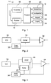
- FIG. 1 is a block schematic diagram of a mobile telephone in accordance with an aspect of the present invention. This is an example of the type of portable communication apparatus, in which the invention can be applied.
- the mobile phone 10 has an antenna 12, which is used for transmitting and receiving radio frequency signals. Received signals are passed to receiver circuitry 14, while transmitted signals are sent to the antenna 12 from transmitter circuitry 16.
- the receiver circuitry 14 and transmitter circuitry 16 are both connected to processor circuitry 18 which, in this case, is used to represent both signal processing circuitry and a control processor which controls the operation of the device.
- the processor circuitry 18 receives audio inputs from a microphone 20, and alphanumeric or other inputs from a keypad 22, and provides audio outputs through a loudspeaker 24, and visual outputs through a display 26.
- FIG. 2 is a block schematic diagram of the relevant parts of the transmitter circuitry 16, which is otherwise conventional, but is described herein only to the extent necessary for an understanding of the present invention.
- the transmitter circuitry includes a voltage controlled oscillator (VCO) 30, which may for example produce an output signal at a frequency in the region of 3.6GHz, with the exact frequency being determined by the channel on which the device is transmitting.
- VCO voltage controlled oscillator
- the VCO output signal is supplied to a digital divider 32 which, under the control of the processor 18 and depending upon the frequency band in which the device is operating, may divide the frequency of the output signal either by two or by four.
- the VCO output signal frequency must be divided by four
- the frequency of the VCO output signal must be divided by two.
- the resulting divider output signal is then supplied to a power amplifier 34. This produces an output signal for supplying to the antenna 12.
- the output power of transmissions from the device must be carefully controlled, and the power amplifier 34 receives a power control input signal from power control circuitry 36.
- This power control signal effectively alters the gain of the power amplifier, so that the power amplifier output signal is at the desired power level.
- the divider 32 introduces a source of noise into the output signal, while the power amplifier 34 inevitably amplifies any noise which is present at its input, whether that originates in the VCO 30, or in the divider 32.
- the GSM specification sets a maximum permissible absolute noise power level in transmitted signals, in order to minimise the possibility that the noise in a transmitted signal will interfere with received signals at a nearby device.
- the power amplifier 34 When the power amplifier 34 is operating with a high gain, in order to ensure that the transmitted signal has a desired relatively high power level, then it also amplifies the noise signal at the same time. Therefore, it is when the power amplifier 34 is operating with high gain that it is most important to ensure that the divider 32 is introducing the smallest possible amount of noise.
- the noise performance of the divider 32 is improved by increasing the bias current supplied to it. However, this obviously increases the power consumption of the device.
- the bias current of the divider 32 is controlled on the basis of the power control signal from the power control circuitry 36 such that, when the power amplifier 34 is operating with high gain, the bias current in the divider 32 is kept relatively high, in order to improve the noise performance of the divider.
- the divider 32 can be operated with a lower bias current, and therefore a worse noise performance, since it will still then be possible to meet the requirements of the specification regarding noise, while reducing power consumption.
- the maximum permitted noise level at the transmitter output is -79dBm. Therefore, in order to meet the specification, the noise generated by the transmitter circuitry after amplification by the power amplifier 34 must be less than -79dBm. This can be expressed N t + G pa ⁇ -79dBm where N t is the noise generated by the transmitter circuitry (including the noise from the divider 32) and G pa is the gain of the power amplifier 34. Therefore when the gain of the power amplifier 34 is low, the noise generated by the divider 32 can be higher than when the gain of the power amplifier 34 is high.
- Figure 3 shows a circuit schematic of the variable current divider 32 in accordance with the invention.
- variable current divider circuit 32 shown here is configured to divide the frequency of the incoming signals by two, although it will be appreciated that the technique described below is also applicable to variable current divider circuitry having other divide ratios.
- the divider circuit comprises a divide-by-2 circuit 102 having signal inputs 104 and signal outputs 106.
- the divide-by-2 circuit 102 is a conventional divider circuit based on flip-flops comprising transistors Q1 to Q12.
- the noise properties of the divider 32 are controlled by the power control signal 108 from the power control circuitry 36.
- the power control signal 108 is a digital signal taking the values of 0 or 1.
- the power control signal has the value 1.
- a poorer noise profile is tolerable, (i.e. low current, high impedance) the power control signal has the value 0.
- the power control signal 108 controls the current at both the collector inputs and emitter outputs of the divide-by-2 circuitry 102 by changing the resistance seen by the divide-by-2 circuitry 102.
- Resistors R1, R2, R9 and R10 are connected between the voltage supply rail and the collector inputs of transistors Q1, Q2, Q7 and Q8 respectively. Connected in parallel with each of the resistors R1, R2, R9 and R10 are a second resistor (R3, R4, R11 and R12 respectively) and a transistor switch (Q13, Q14, Q15 and Q16 respectively). The base of each of the transistor switches Q13, Q14, Q15 and Q16 is controlled by the power control signal 108.
- Resistor R18 is connected between ground and the combined emitter outputs of transistors Q5 and Q6.
- Resistor R17 is connected between ground and the combined emitter outputs of Q9 and Q12.
- Connected in parallel with each of resistors R18 and R17 is a second resistor (R19 and R20 respectively) and a transistor switch (Q17 and Q18 respectively). The base of each of the transistor switches Q17 and Q18 is controlled by the power control signal 108.
- the base of the transistor switches Q13, Q14, Q15, Q16, Q17 and Q18 are 0, and the switches are off. Therefore, the impedances at the collectors of transistors Q1, Q2, Q7 and Q8 will be R1, R2, R9 and R10 respectively.
- the impedances at the combined emitter outputs of Q5 and Q6 and Q9 and Q12 will be R18 and R17 respectively.
- the transistor switches Q13, Q14, Q15, Q16, Q17 and Q18 will be on. Therefore, the impedances at the collectors of transistors Q1, Q2, Q7 and Q8 and at the combined emitter outputs of Q5 and Q6 and Q9 and Q12 will be reduced since resistors R1, R2, R9, R10, R18 and R17 are now in parallel with resistors R3, R4, R11, R12, R19 and R20 respectively. Therefore the effective impedance is reduced, and the current is increased, providing a better noise profile.
- FIG 4 shows an alternative embodiment of the transmit circuitry 16, in which elements which have the same function as elements in the circuitry of Figure 2 are illustrated by the same reference numerals, and will not be described further.
- divider circuits 40, 42 there are two divider circuits 40, 42, each of which may be programmable to divide the frequency of incoming signals either by two or by four, as described above in the case of the divider 32 shown in Figure 2.
- the divider circuits 40, 42 are biased for high current operation and for low current operation respectively.
- each of the divider circuits 40, 42 comprise a fixed current divider circuit as shown in Figure 5.
- the fixed current divider circuit shown here is configured to divide the frequency of the incoming signals by two, although it will be appreciated that the technique described below is also applicable to divider circuitry having other divide ratios.
- the divider circuit comprises a divide-by-2 circuit 102 having signal inputs 104 and signal outputs 106.
- the divide-by-2 circuit 102 is a conventional divider circuit based on flip-flops comprising transistors Q1 to Q12.
- Resistors R30, R31, R32 and R33 are connected between the positive voltage rail and the collectors of transistors Q1, Q2, Q7 and Q8 respectively.
- Resistor R34 is connected between ground and the combined emitter outputs of transistors Q5 and Q6.
- Resistor R35 is connected between ground and the combined emitter outputs of Q9 and Q12.
- the values of the resistors are chosen so that the impedance of the divider circuitry 40 is low.
- the values of the resistors can be chosen so that the impedance of the divider circuitry 42 is high.
- the divider 40 is selected, since this has a relatively good noise performance.
- the power control signal from the power control circuitry 36 indicates that the power amplifier 34 is to operate with lower gain, and hence that there will be less amplification of the noise signals, the divider 42 is selected, since it is then sufficient for the worse noise performance of this device to be used.
- FIG. 6 is a flow chart illustrating a method of operation of the transmitter circuitry as shown in Figure 2 or Figure 4.
- the processor circuitry determines the required output signal power to be transmitted. On the basis of the required signal power, the circuitry then determines the acceptable noise performance for the divider circuitry, in step 62, and, in step 64, controls the divider current appropriately.
- this control may take the form of adjusting the bias current to the divider circuit, or may take the form of selecting a divider circuit from a plurality of available divider circuits, which have bias currents which are appropriate for different required noise performances.
- the determination in step 62 may be carried out by means of a mathematical calculation or, more conveniently, can for example be made by comparing the level of the power control signal with a threshold, in order to determine whether the divider circuitry should be operated with a relatively good noise performance, or with a worse noise performance.
- the following example of a GSM radio transmitter is provided.
- all elements in the radio transmitter are assumed to be ideal and noiseless, except for the divider output resistors, which generate thermal noise.
- the input impedance of the power amplifier is assumed to be much higher than the output impedance of the divider, so the power amplifier responds to the voltage at the divider output.
- the output of the divider is modelled as a voltage source with a real resistive impedance of 60ohms.
- the output voltage at the required carrier frequency is assumed to be 0.4V peak to peak.
- the collector load resistors are expected to be the dominant noise source of the divider (as mentioned above, in a real design other sources of noise are present).
- Kb Boltzmann's constant
- Kb a bandwidth of 100KHz
- room temperature of 298K the RMS thermal noise voltage
- the GSM specification for the noise level at the transmitter output is -79dBm, and so the -117.046dBm noise level can be amplified by about 38dB before it fails the GSM specification. From the previous reasoning, this noise level is adequate since a gain of 37dB is required to reach the required maximum level for a class 4 handset.
- the power consumption of the divider can be reduced dynamically when the power amplifier is operating with a lower gain as greater noise from the divider can be tolerated.
- the collector resistor values were doubled to 120ohms, while maintaining the same voltage at the output of the divider, the divider current will be halved.
- the noise level of the divider circuit is 3dB higher.
- transmitter circuitry which can ensure that a specified noise requirement is met, without excessively increasing the power consumption or the size of the device.
Landscapes
- Engineering & Computer Science (AREA)
- Power Engineering (AREA)
- Computer Networks & Wireless Communication (AREA)
- Signal Processing (AREA)
- Transmitters (AREA)
- Transceivers (AREA)
- Details Of Aerials (AREA)
- Amplifiers (AREA)
Priority Applications (9)
| Application Number | Priority Date | Filing Date | Title |
|---|---|---|---|
| EP03251667A EP1460767B1 (fr) | 2003-03-18 | 2003-03-18 | Emetteur radio |
| AT03251667T ATE296499T1 (de) | 2003-03-18 | 2003-03-18 | Funksender |
| DE60300716T DE60300716T2 (de) | 2003-03-18 | 2003-03-18 | Funksender |
| JP2006504712A JP4520458B2 (ja) | 2003-03-18 | 2004-03-17 | 無線送信機 |
| CNA2004800073952A CN1762104A (zh) | 2003-03-18 | 2004-03-17 | 无线电发射器 |
| KR1020057017201A KR101030913B1 (ko) | 2003-03-18 | 2004-03-17 | 무선 송신기 |
| PCT/EP2004/002762 WO2004084425A1 (fr) | 2003-03-18 | 2004-03-17 | Emetteur radio |
| US10/548,206 US7412216B2 (en) | 2003-03-18 | 2004-03-17 | Radio transmitter |
| US12/168,357 US8320845B2 (en) | 2003-03-18 | 2008-07-07 | Radio transmitter |
Applications Claiming Priority (1)
| Application Number | Priority Date | Filing Date | Title |
|---|---|---|---|
| EP03251667A EP1460767B1 (fr) | 2003-03-18 | 2003-03-18 | Emetteur radio |
Publications (2)
| Publication Number | Publication Date |
|---|---|
| EP1460767A1 true EP1460767A1 (fr) | 2004-09-22 |
| EP1460767B1 EP1460767B1 (fr) | 2005-05-25 |
Family
ID=32799058
Family Applications (1)
| Application Number | Title | Priority Date | Filing Date |
|---|---|---|---|
| EP03251667A Expired - Lifetime EP1460767B1 (fr) | 2003-03-18 | 2003-03-18 | Emetteur radio |
Country Status (8)
| Country | Link |
|---|---|
| US (1) | US7412216B2 (fr) |
| EP (1) | EP1460767B1 (fr) |
| JP (1) | JP4520458B2 (fr) |
| KR (1) | KR101030913B1 (fr) |
| CN (1) | CN1762104A (fr) |
| AT (1) | ATE296499T1 (fr) |
| DE (1) | DE60300716T2 (fr) |
| WO (1) | WO2004084425A1 (fr) |
Cited By (2)
| Publication number | Priority date | Publication date | Assignee | Title |
|---|---|---|---|---|
| WO2012014060A1 (fr) * | 2010-07-29 | 2012-02-02 | Marvell World Trade Ltd. | Configuration de diviseur et de mélangeur de fréquence modulaire |
| US9325541B2 (en) | 2010-07-29 | 2016-04-26 | Marvell World Trade Ltd. | Modular frequency divider with switch configuration to reduce parasitic capacitance |
Families Citing this family (4)
| Publication number | Priority date | Publication date | Assignee | Title |
|---|---|---|---|---|
| US8320845B2 (en) * | 2003-03-18 | 2012-11-27 | Telefonaktiebolaget L M Ericsson (Publ) | Radio transmitter |
| EP2052512A2 (fr) * | 2006-08-04 | 2009-04-29 | Telefonaktiebolaget LM Ericsson (PUBL) | Gestion de politique dans des scénarios multi-accès |
| DE102007046341A1 (de) * | 2007-09-27 | 2009-04-23 | Infineon Technologies Ag | Schaltungsanordnung zum Verarbeiten eines hochfrequenten Signals |
| FI20075715A0 (fi) * | 2007-10-09 | 2007-10-09 | Nokia Corp | Taajuusjakajan konfiguraatio |
Citations (2)
| Publication number | Priority date | Publication date | Assignee | Title |
|---|---|---|---|---|
| US5697073A (en) * | 1994-08-26 | 1997-12-09 | Motorola, Inc. | Apparatus and method for shaping and power controlling a signal in a transmitter |
| US5894592A (en) * | 1997-04-17 | 1999-04-13 | Motorala, Inc. | Wideband frequency synthesizer for direct conversion transceiver |
Family Cites Families (15)
| Publication number | Priority date | Publication date | Assignee | Title |
|---|---|---|---|---|
| US4969210A (en) * | 1988-02-10 | 1990-11-06 | Motorola, Inc. | Two-way radio having a PLL |
| JPH07101820B2 (ja) * | 1989-12-27 | 1995-11-01 | 三菱電機株式会社 | 低歪高周波増幅装置 |
| GB9017068D0 (en) * | 1990-08-03 | 1990-09-19 | Marconi Instruments Ltd | Low noise frequency divider architecture |
| US5598405A (en) * | 1994-01-25 | 1997-01-28 | Alps Electric Co., Ltd. | Time division multiple access time division duplex type transmitter-receiver |
| US5586146A (en) * | 1995-01-30 | 1996-12-17 | Motorola, Inc. | Programmable voltage controlled attenuator |
| US6253068B1 (en) * | 1997-05-09 | 2001-06-26 | Micrel, Incorporated | Fully integrated all-CMOS AM transmitter with automatic antenna tuning |
| KR100234129B1 (ko) * | 1997-06-21 | 1999-12-15 | 윤종용 | 시분할 교신 방식을 사용하는 디지탈 무선통신장치 및 방법 |
| JPH1132260A (ja) * | 1997-07-09 | 1999-02-02 | Akira Kamimura | Fm電波によるビデオ信号送受信システム |
| FR2787257A1 (fr) * | 1998-12-15 | 2000-06-16 | Koninkl Philips Electronics Nv | Appareil radioelectrique comportant un synthetiseur de frequences et procede pour moduler en phase et/ou en frequence un synthetiseur de frequences |
| TW527763B (en) * | 2000-05-01 | 2003-04-11 | Koninkl Philips Electronics Nv | Power adaptive frequency divider |
| KR100667641B1 (ko) * | 2000-11-03 | 2007-01-12 | 퀄컴 인코포레이티드 | 전송기 이득에 기초한 전송기 바이어스 전류의 조정 |
| JP3851511B2 (ja) * | 2001-03-14 | 2006-11-29 | 株式会社ルネサステクノロジ | Fm送信機 |
| US6509800B2 (en) * | 2001-04-03 | 2003-01-21 | Agilent Technologies, Inc. | Polyphase noise-shaping fractional-N frequency synthesizer |
| US7046972B2 (en) * | 2001-04-10 | 2006-05-16 | Matsushita Electric Industrial Co., Ltd. | Predistortion linearizer and predistortion distortion compensation method, program, and medium |
| GB2389275B (en) * | 2002-05-31 | 2006-10-25 | Hitachi Ltd | Apparatus for mobile communication system |
-
2003
- 2003-03-18 DE DE60300716T patent/DE60300716T2/de not_active Expired - Lifetime
- 2003-03-18 AT AT03251667T patent/ATE296499T1/de not_active IP Right Cessation
- 2003-03-18 EP EP03251667A patent/EP1460767B1/fr not_active Expired - Lifetime
-
2004
- 2004-03-17 KR KR1020057017201A patent/KR101030913B1/ko not_active Expired - Fee Related
- 2004-03-17 WO PCT/EP2004/002762 patent/WO2004084425A1/fr not_active Ceased
- 2004-03-17 CN CNA2004800073952A patent/CN1762104A/zh active Pending
- 2004-03-17 JP JP2006504712A patent/JP4520458B2/ja not_active Expired - Fee Related
- 2004-03-17 US US10/548,206 patent/US7412216B2/en not_active Expired - Lifetime
Patent Citations (2)
| Publication number | Priority date | Publication date | Assignee | Title |
|---|---|---|---|---|
| US5697073A (en) * | 1994-08-26 | 1997-12-09 | Motorola, Inc. | Apparatus and method for shaping and power controlling a signal in a transmitter |
| US5894592A (en) * | 1997-04-17 | 1999-04-13 | Motorala, Inc. | Wideband frequency synthesizer for direct conversion transceiver |
Non-Patent Citations (1)
| Title |
|---|
| WEGER P ET AL: "Completely Integrated 1.5 Ghz Direct Conversion Transceiver", PAGE(S) 135-136, XP010221223 * |
Cited By (4)
| Publication number | Priority date | Publication date | Assignee | Title |
|---|---|---|---|---|
| WO2012014060A1 (fr) * | 2010-07-29 | 2012-02-02 | Marvell World Trade Ltd. | Configuration de diviseur et de mélangeur de fréquence modulaire |
| US8442462B2 (en) | 2010-07-29 | 2013-05-14 | Marvell World Trade Ltd. | Modular frequency divider and mixer configuration |
| US8965310B2 (en) | 2010-07-29 | 2015-02-24 | Marvell World Trade Ltd. | Modular frequency divider and mixer configuration |
| US9325541B2 (en) | 2010-07-29 | 2016-04-26 | Marvell World Trade Ltd. | Modular frequency divider with switch configuration to reduce parasitic capacitance |
Also Published As
| Publication number | Publication date |
|---|---|
| WO2004084425A1 (fr) | 2004-09-30 |
| US7412216B2 (en) | 2008-08-12 |
| ATE296499T1 (de) | 2005-06-15 |
| US20070037533A1 (en) | 2007-02-15 |
| KR20050115284A (ko) | 2005-12-07 |
| KR101030913B1 (ko) | 2011-04-22 |
| CN1762104A (zh) | 2006-04-19 |
| DE60300716T2 (de) | 2005-10-20 |
| EP1460767B1 (fr) | 2005-05-25 |
| DE60300716D1 (de) | 2005-06-30 |
| JP4520458B2 (ja) | 2010-08-04 |
| JP2006520560A (ja) | 2006-09-07 |
Similar Documents
| Publication | Publication Date | Title |
|---|---|---|
| RU2252483C2 (ru) | Способ и устройство усиления мощности передачи беспроводного телефона при пониженном энергопотреблении | |
| KR100312367B1 (ko) | 이동체통신장치및방법 | |
| US9405332B2 (en) | RF power amplifier with linearity control | |
| TWI235545B (en) | Gain linearizer for variable gain amplifiers | |
| US7741904B2 (en) | Efficient integrated linear amplifier module | |
| JP2005518684A (ja) | 電力増幅器の制御 | |
| US10033340B1 (en) | Low-noise amplifier (LNA) with capacitive attenuator | |
| JP2004500781A (ja) | Rf電力増幅器用の動的バイアス | |
| JP4931936B2 (ja) | 送信装置及び通信装置 | |
| RU2209504C2 (ru) | Усилитель с переменным усилением и высоким динамическим диапазоном | |
| JP2000209049A (ja) | 通信装置内の増幅器を選択するシステムおよび方法 | |
| KR100251560B1 (ko) | 부호분할 다중 접속방식 단말기의 외부 간섭신호 제거장치 | |
| US6122491A (en) | Communications system using power amplifier with dynamic biasing | |
| JP2010273069A (ja) | 受信器、送受信器および携帯端末装置 | |
| EP1460767B1 (fr) | Emetteur radio | |
| US20070270111A1 (en) | Dual power mode transmitter | |
| US5873046A (en) | System for communicating in analog or digital mode and mobile station employing the same | |
| US8320845B2 (en) | Radio transmitter | |
| EP1122883A2 (fr) | Circuit de linéarisation d'un profil de contrôle de puissance d'un amplificateur de puissance BiCMOS | |
| GB2362523A (en) | A transceiver with the bias of an amplifier in the receiver controlled by a baseband processor | |
| US7348852B1 (en) | Device and method for power amplifier noise reduction | |
| EP1175732A1 (fr) | Systeme et procede pour la commande selective du fonctionnement d'un amplificateur | |
| JPH07336268A (ja) | デュアルモード無線機 | |
| Jianhai et al. | The design of AGC in RF receiver for WCDMA base station | |
| Wong et al. | RF transceiver reference design for third generation W-CDMA cellular handset |
Legal Events
| Date | Code | Title | Description |
|---|---|---|---|
| PUAI | Public reference made under article 153(3) epc to a published international application that has entered the european phase |
Free format text: ORIGINAL CODE: 0009012 |
|
| 17P | Request for examination filed |
Effective date: 20031105 |
|
| AK | Designated contracting states |
Kind code of ref document: A1 Designated state(s): AT BE BG CH CY CZ DE DK EE ES FI FR GB GR HU IE IT LI LU MC NL PT SE SI SK TR |
|
| AX | Request for extension of the european patent |
Extension state: AL LT LV MK RO |
|
| GRAP | Despatch of communication of intention to grant a patent |
Free format text: ORIGINAL CODE: EPIDOSNIGR1 |
|
| GRAS | Grant fee paid |
Free format text: ORIGINAL CODE: EPIDOSNIGR3 |
|
| GRAA | (expected) grant |
Free format text: ORIGINAL CODE: 0009210 |
|
| AK | Designated contracting states |
Kind code of ref document: B1 Designated state(s): AT BE BG CH CY CZ DE DK EE ES FI FR GB GR HU IE IT LI LU MC NL PT SE SI SK TR |
|
| AX | Request for extension of the european patent |
Extension state: AL LT LV MK RO |
|
| PG25 | Lapsed in a contracting state [announced via postgrant information from national office to epo] |
Ref country code: CH Free format text: LAPSE BECAUSE OF FAILURE TO SUBMIT A TRANSLATION OF THE DESCRIPTION OR TO PAY THE FEE WITHIN THE PRESCRIBED TIME-LIMIT Effective date: 20050525 Ref country code: SI Free format text: LAPSE BECAUSE OF FAILURE TO SUBMIT A TRANSLATION OF THE DESCRIPTION OR TO PAY THE FEE WITHIN THE PRESCRIBED TIME-LIMIT Effective date: 20050525 Ref country code: IT Free format text: LAPSE BECAUSE OF FAILURE TO SUBMIT A TRANSLATION OF THE DESCRIPTION OR TO PAY THE FEE WITHIN THE PRESCRIBED TIME-LIMIT;WARNING: LAPSES OF ITALIAN PATENTS WITH EFFECTIVE DATE BEFORE 2007 MAY HAVE OCCURRED AT ANY TIME BEFORE 2007. THE CORRECT EFFECTIVE DATE MAY BE DIFFERENT FROM THE ONE RECORDED. Effective date: 20050525 Ref country code: AT Free format text: LAPSE BECAUSE OF FAILURE TO SUBMIT A TRANSLATION OF THE DESCRIPTION OR TO PAY THE FEE WITHIN THE PRESCRIBED TIME-LIMIT Effective date: 20050525 Ref country code: FI Free format text: LAPSE BECAUSE OF FAILURE TO SUBMIT A TRANSLATION OF THE DESCRIPTION OR TO PAY THE FEE WITHIN THE PRESCRIBED TIME-LIMIT Effective date: 20050525 Ref country code: CZ Free format text: LAPSE BECAUSE OF FAILURE TO SUBMIT A TRANSLATION OF THE DESCRIPTION OR TO PAY THE FEE WITHIN THE PRESCRIBED TIME-LIMIT Effective date: 20050525 Ref country code: NL Free format text: LAPSE BECAUSE OF FAILURE TO SUBMIT A TRANSLATION OF THE DESCRIPTION OR TO PAY THE FEE WITHIN THE PRESCRIBED TIME-LIMIT Effective date: 20050525 Ref country code: SK Free format text: LAPSE BECAUSE OF FAILURE TO SUBMIT A TRANSLATION OF THE DESCRIPTION OR TO PAY THE FEE WITHIN THE PRESCRIBED TIME-LIMIT Effective date: 20050525 Ref country code: LI Free format text: LAPSE BECAUSE OF FAILURE TO SUBMIT A TRANSLATION OF THE DESCRIPTION OR TO PAY THE FEE WITHIN THE PRESCRIBED TIME-LIMIT Effective date: 20050525 Ref country code: BE Free format text: LAPSE BECAUSE OF FAILURE TO SUBMIT A TRANSLATION OF THE DESCRIPTION OR TO PAY THE FEE WITHIN THE PRESCRIBED TIME-LIMIT Effective date: 20050525 |
|
| REG | Reference to a national code |
Ref country code: GB Ref legal event code: FG4D |
|
| REG | Reference to a national code |
Ref country code: CH Ref legal event code: EP |
|
| AKX | Designation fees paid |
Designated state(s): AT BE BG CH CY CZ DE DK EE ES FI FR GB GR HU IE IT LI LU MC NL PT SE SI SK TR |
|
| REG | Reference to a national code |
Ref country code: IE Ref legal event code: FG4D |
|
| REF | Corresponds to: |
Ref document number: 60300716 Country of ref document: DE Date of ref document: 20050630 Kind code of ref document: P |
|
| PG25 | Lapsed in a contracting state [announced via postgrant information from national office to epo] |
Ref country code: GR Free format text: LAPSE BECAUSE OF FAILURE TO SUBMIT A TRANSLATION OF THE DESCRIPTION OR TO PAY THE FEE WITHIN THE PRESCRIBED TIME-LIMIT Effective date: 20050825 Ref country code: DK Free format text: LAPSE BECAUSE OF FAILURE TO SUBMIT A TRANSLATION OF THE DESCRIPTION OR TO PAY THE FEE WITHIN THE PRESCRIBED TIME-LIMIT Effective date: 20050825 Ref country code: SE Free format text: LAPSE BECAUSE OF FAILURE TO SUBMIT A TRANSLATION OF THE DESCRIPTION OR TO PAY THE FEE WITHIN THE PRESCRIBED TIME-LIMIT Effective date: 20050825 Ref country code: BG Free format text: LAPSE BECAUSE OF FAILURE TO SUBMIT A TRANSLATION OF THE DESCRIPTION OR TO PAY THE FEE WITHIN THE PRESCRIBED TIME-LIMIT Effective date: 20050825 |
|
| PG25 | Lapsed in a contracting state [announced via postgrant information from national office to epo] |
Ref country code: ES Free format text: LAPSE BECAUSE OF FAILURE TO SUBMIT A TRANSLATION OF THE DESCRIPTION OR TO PAY THE FEE WITHIN THE PRESCRIBED TIME-LIMIT Effective date: 20050905 |
|
| PG25 | Lapsed in a contracting state [announced via postgrant information from national office to epo] |
Ref country code: PT Free format text: LAPSE BECAUSE OF FAILURE TO SUBMIT A TRANSLATION OF THE DESCRIPTION OR TO PAY THE FEE WITHIN THE PRESCRIBED TIME-LIMIT Effective date: 20051027 |
|
| PG25 | Lapsed in a contracting state [announced via postgrant information from national office to epo] |
Ref country code: HU Free format text: LAPSE BECAUSE OF FAILURE TO SUBMIT A TRANSLATION OF THE DESCRIPTION OR TO PAY THE FEE WITHIN THE PRESCRIBED TIME-LIMIT Effective date: 20051126 |
|
| REG | Reference to a national code |
Ref country code: CH Ref legal event code: PL |
|
| NLV1 | Nl: lapsed or annulled due to failure to fulfill the requirements of art. 29p and 29m of the patents act | ||
| PG25 | Lapsed in a contracting state [announced via postgrant information from national office to epo] |
Ref country code: IE Free format text: LAPSE BECAUSE OF NON-PAYMENT OF DUE FEES Effective date: 20060320 |
|
| PG25 | Lapsed in a contracting state [announced via postgrant information from national office to epo] |
Ref country code: MC Free format text: LAPSE BECAUSE OF NON-PAYMENT OF DUE FEES Effective date: 20060331 Ref country code: LU Free format text: LAPSE BECAUSE OF NON-PAYMENT OF DUE FEES Effective date: 20060331 |
|
| PLBE | No opposition filed within time limit |
Free format text: ORIGINAL CODE: 0009261 |
|
| STAA | Information on the status of an ep patent application or granted ep patent |
Free format text: STATUS: NO OPPOSITION FILED WITHIN TIME LIMIT |
|
| 26N | No opposition filed |
Effective date: 20060228 |
|
| EN | Fr: translation not filed | ||
| REG | Reference to a national code |
Ref country code: IE Ref legal event code: MM4A |
|
| PG25 | Lapsed in a contracting state [announced via postgrant information from national office to epo] |
Ref country code: EE Free format text: LAPSE BECAUSE OF FAILURE TO SUBMIT A TRANSLATION OF THE DESCRIPTION OR TO PAY THE FEE WITHIN THE PRESCRIBED TIME-LIMIT Effective date: 20050525 |
|
| PG25 | Lapsed in a contracting state [announced via postgrant information from national office to epo] |
Ref country code: TR Free format text: LAPSE BECAUSE OF FAILURE TO SUBMIT A TRANSLATION OF THE DESCRIPTION OR TO PAY THE FEE WITHIN THE PRESCRIBED TIME-LIMIT Effective date: 20050525 |
|
| PG25 | Lapsed in a contracting state [announced via postgrant information from national office to epo] |
Ref country code: FR Free format text: LAPSE BECAUSE OF FAILURE TO SUBMIT A TRANSLATION OF THE DESCRIPTION OR TO PAY THE FEE WITHIN THE PRESCRIBED TIME-LIMIT Effective date: 20050525 Ref country code: CY Free format text: LAPSE BECAUSE OF FAILURE TO SUBMIT A TRANSLATION OF THE DESCRIPTION OR TO PAY THE FEE WITHIN THE PRESCRIBED TIME-LIMIT Effective date: 20050525 |
|
| PGFP | Annual fee paid to national office [announced via postgrant information from national office to epo] |
Ref country code: GB Payment date: 20220328 Year of fee payment: 20 Ref country code: DE Payment date: 20220329 Year of fee payment: 20 |
|
| REG | Reference to a national code |
Ref country code: DE Ref legal event code: R071 Ref document number: 60300716 Country of ref document: DE |
|
| REG | Reference to a national code |
Ref country code: GB Ref legal event code: PE20 Expiry date: 20230317 |
|
| PG25 | Lapsed in a contracting state [announced via postgrant information from national office to epo] |
Ref country code: GB Free format text: LAPSE BECAUSE OF EXPIRATION OF PROTECTION Effective date: 20230317 |