EP1465059A2 - Vorrichtung und Verfahren zum Umbenennen einer Cachespeicherzeile - Google Patents
Vorrichtung und Verfahren zum Umbenennen einer Cachespeicherzeile Download PDFInfo
- Publication number
- EP1465059A2 EP1465059A2 EP03257877A EP03257877A EP1465059A2 EP 1465059 A2 EP1465059 A2 EP 1465059A2 EP 03257877 A EP03257877 A EP 03257877A EP 03257877 A EP03257877 A EP 03257877A EP 1465059 A2 EP1465059 A2 EP 1465059A2
- Authority
- EP
- European Patent Office
- Prior art keywords
- cache line
- cache
- instruction
- prefetch
- microprocessor
- Prior art date
- Legal status (The legal status is an assumption and is not a legal conclusion. Google has not performed a legal analysis and makes no representation as to the accuracy of the status listed.)
- Granted
Links
Images





Classifications
-
- G—PHYSICS
- G06—COMPUTING OR CALCULATING; COUNTING
- G06F—ELECTRIC DIGITAL DATA PROCESSING
- G06F9/00—Arrangements for program control, e.g. control units
- G06F9/06—Arrangements for program control, e.g. control units using stored programs, i.e. using an internal store of processing equipment to receive or retain programs
- G06F9/30—Arrangements for executing machine instructions, e.g. instruction decode
- G06F9/30003—Arrangements for executing specific machine instructions
- G06F9/30007—Arrangements for executing specific machine instructions to perform operations on data operands
- G06F9/30032—Movement instructions, e.g. MOVE, SHIFT, ROTATE, SHUFFLE
-
- G—PHYSICS
- G06—COMPUTING OR CALCULATING; COUNTING
- G06F—ELECTRIC DIGITAL DATA PROCESSING
- G06F12/00—Accessing, addressing or allocating within memory systems or architectures
- G06F12/02—Addressing or allocation; Relocation
- G06F12/08—Addressing or allocation; Relocation in hierarchically structured memory systems, e.g. virtual memory systems
- G06F12/0802—Addressing of a memory level in which the access to the desired data or data block requires associative addressing means, e.g. caches
- G06F12/0806—Multiuser, multiprocessor or multiprocessing cache systems
- G06F12/0815—Cache consistency protocols
-
- G—PHYSICS
- G06—COMPUTING OR CALCULATING; COUNTING
- G06F—ELECTRIC DIGITAL DATA PROCESSING
- G06F12/00—Accessing, addressing or allocating within memory systems or architectures
- G06F12/02—Addressing or allocation; Relocation
- G06F12/08—Addressing or allocation; Relocation in hierarchically structured memory systems, e.g. virtual memory systems
- G06F12/0802—Addressing of a memory level in which the access to the desired data or data block requires associative addressing means, e.g. caches
- G06F12/0862—Addressing of a memory level in which the access to the desired data or data block requires associative addressing means, e.g. caches with prefetch
-
- G—PHYSICS
- G06—COMPUTING OR CALCULATING; COUNTING
- G06F—ELECTRIC DIGITAL DATA PROCESSING
- G06F9/00—Arrangements for program control, e.g. control units
- G06F9/06—Arrangements for program control, e.g. control units using stored programs, i.e. using an internal store of processing equipment to receive or retain programs
- G06F9/30—Arrangements for executing machine instructions, e.g. instruction decode
- G06F9/30003—Arrangements for executing specific machine instructions
- G06F9/3004—Arrangements for executing specific machine instructions to perform operations on memory
-
- G—PHYSICS
- G06—COMPUTING OR CALCULATING; COUNTING
- G06F—ELECTRIC DIGITAL DATA PROCESSING
- G06F2212/00—Indexing scheme relating to accessing, addressing or allocation within memory systems or architectures
- G06F2212/60—Details of cache memory
- G06F2212/6028—Prefetching based on hints or prefetch instructions
Definitions
- the speed at which data can be transferred between internal logic blocks is an order of magnitude faster than the speed that external memory accesses exhibit.
- the bus which interfaces to system memory operates at speeds on the order of hundreds of megahertz while internal microprocessor clock speeds are approaching the tens of gigahertz. Consequently, a hierarchy of cache structures has evolved over more recent years to allow high-performance microprocessors to run at speed without having to stall while transactions are executed over a slow memory bus every time data is to be read or written.
- a primary microprocessor communicates with a communications microprocessor by reading data from and writing data to a specified region of memory. It is also very common to find areas of memory known as video buffers that are shared between a primary microprocessor and a microprocessor on a video card that is responsible for displaying data to an operator on a video device.
- FIGURE 6 is a block diagram detailing a microprocessor according to the present invention for performing a prefetch-with-intent-to-store operation
- FIGURE 15 is a block diagram depicting a cache unit interface to memory for allocating and renaming a cache line within the microprocessor of FIGURE 6;
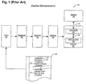
- the execute stage 105 performs the operations that are specified by the micro instructions.
- the types of operations vary according to instruction set architecture, however one skilled in the art will appreciate that these operations fall into general categories such as logical operations, arithmetic operations, and memory access operations (i.e., data read and data write operations). Results generated by performing the prescribed operations are either stored back into registers in the register stage 103 or they are written to locations in data memory 108.
- a present day microprocessor 100 provides a data cache 107 within the execute stage 105 along with execute logic 106.
- the data cache 107 operates in parallel with the execution of instructions in the pipeline stages 101-105 to ensure that data which has a high probability of being accessed by the instructions 121-123 of an application program are present within the cache 107 so that when a data access micro instruction (i.e., a load memory or store memory micro instruction) proceeds through the execute stage 105, the execute logic 106 is able to execute the data access in one or two pipeline clock cycles rather than incurring a program delay of perhaps hundreds of clock cycles while waiting for the data access to be executed to system data memory 108 over a memory bus 110.
- a data access micro instruction i.e., a load memory or store memory micro instruction
- cache line widths i.e., the size of a cache line in bytes
- a cache line within a local data cache 107 may be in one of four states: modified, exclusive, shared, and invalid.
- a modified line is one to which a local store operation has been executed, but which has not yet been synchronized with (i.e., written back to) main memory 108. It is the responsibility of a local cache 107 to monitor memory transactions over the memory bus 110 from other devices (also known as bus agents) so that if they request data from a modified cache line, the local cache 107 provides the modified data to the requesting bus agent. This monitoring of the bus 110 is known as bus snooping.
- a cache line in the exclusive state is one to which the local cache 107 may execute a store operation.
- the exclusive state implies that the local cache 107 possesses exclusive ownership of the cache line; the microprocessor 100 is thus allowed modify its contents.
- a shared cache line is one that is resident within the local caches 107 of two or more devices on the bus 110. As such, each device may read data from a shared cache line, but they are not allowed to modify its contents.
- a device 100 In order to modify data (i.e., to execute a store operation) in a shared cache line, a device 100 must first conduct appropriate transactions over the memory bus 110 with the other bus agents to obtain exclusive ownership of the cache line (i.e., to read the cache line into its cache 107 in the exclusive MESI state) prior to modifying its contents. Once exclusive ownership of the line is obtained, then the store operation may be executed and the cache line state is changed to modified. Requiring exclusive ownership of a cache line before posting store operations guarantees data consistency in that only one device 100 can modify the contents of a cache line at any point in time.
- a cache line's state is changed to invalid when the local cache 107 detects (by snooping) a write transaction over the memory bus 110 to that cache line, or when a bus transaction is issued over the bus 110 by another device to obtain exclusive ownership of the line. Marking a line as invalid indicates that the data within is not to be read or written because it is most likely inconsistent with memory 108.
- prefetch macro instructions 122 that allow a programmer to direct a microprocessor 100 to load data into a cache 107 before access to the data is required in a program flow 120, thereby overcoming the delay that would be otherwise incurred when data is retrieved from memory 108 into the cache 107 as a result of direct execution of a load instruction in a program flow 120.
- a prefetch instruction 122 is generally provided in a program flow 120 to direct the local data cache 107 to load a cache line from memory 108 in parallel with the execution of subsequent instructions so that the cache line will be in the cache 107 at the point in the program flow 120 where an instruction 123 accesses data from within the cache line.
- a prefetch instruction 122, PREFETCHTO [EAX] directs that the cache line addressed by the contents of register EAX be loaded into cache 107 so that its contents will be available when a subsequent data access instruction 123, MOV EBX,[EAX], is executed in the program flow 120 that directs the microprocessor 100 to read data from an address prescribed by register EAX and move it to register EBX.
- a block diagram 200 depicting a cache unit interface to memory for performing a prefetch operation within the microprocessor of FIGURE 1.
- the block diagram 200 shows logic within the microprocessor 201 that is employed to perform the prefetch operation.
- the microprocessor 201 has a translator 210 that receives a flow of macro instructions 202 and translates the macro instructions 202 into associated micro instructions 211.
- Micro instructions 211 that direct data load and store operations from and to memory 242 are subsequently provided to a cache unit 220.
- the cache unit 220 includes fill logic 221 and a data cache 222.
- the fill logic 221 is coupled to a bus unit 230.
- the bus unit 230 interfaces to a system memory bus 240, to which the data memory 242 and other bus agents 241 are coupled.
- An exemplary flow of macro instructions 202 illustrates how a prefetch operation is prescribed and how subsequent read and store operations may be conducted on the prefetched data.
- a common example of this sequence of operations on a desktop computer is where a counter in memory is read and incremented.
- a sequence of prefetch, read, and store operations recognizes a need to both read data and to subsequently modify data within a cache line.
- a first macro instruction 202, PREFETCH [EAX] in the exemplary flow directs the microprocessor 201 to prefetch the cache line whose address corresponds to the contents of register EAX.
- the fourth macro instruction 202 in the flow is translated into a store micro instruction 211, ST [EAX],EBX, that directs the execute logic to perform a data store operation to write the contents of register EBX into the memory location addressed by the contents of register EAX.
- the store micro instruction 211 is thus provided to the cache unit 220 as a pending store operation. Accordingly, the fill logic 221 detects that the cache line targeted for the pending store operation is present in the data cache 222. If the cache line is in the exclusive state, then the pending store may be immediately posted and the line's state is changed to modified.
- the cache unit 220 asserts a stall signal 223 to halt the progression of micro instructions 211 through the pipeline stages of the microprocessor 201 while the fill logic 221 directs the bus unit 230 to conduct transactions over the system bus 240 to obtain exclusive ownership of the cache line. Once exclusive ownership is obtained, the pending store is allowed to post its data to the cache line and the stall signal is terminated, thereby allowing program execution to resume.
- FIGURE 3 a timing diagram is presented that illustrates the two possible sets 301, 302 of bus transactions which are issued over a memory bus 240 by the microprocessor 201 of FIGURES 1 and 2 to perform a prefetch and subsequent store operation.
- the two sets 301, 302 of transactions include request transactions 303 from the bus unit 230 to the memory bus 240 and response transactions 304 from the memory bus 240 back to the bus unit 230 within the microprocessor 201.
- Transaction set 301 depicts those transactions 303-304 that are conducted when a requested cache line is provided exclusively as a response to a prefetch operation;
- transaction set 302 depicts those transactions 303-304 that are conducted when the requested line is provided in a shared MESI state in response to the prefetch.
- the fill logic 221 directs the bus unit 230 to issue a data read request 303, DATA READ [EAX], to the memory bus 240 requesting that the cache line prescribed by register EAX be provided to the local cache 222.
- the data read request 303 is issued at time A in set 301 and time D in set 302.
- the memory bus 240 sends a data response 304 back to the bus unit 230 that includes the requested cache line. If the cache line is provided exclusively, then the data response 304, DATA RESP [EAX].E, of set 301 is sent back at time B to the bus unit 230. If the cache line is shared, then the data response 304, DATA RESP [EAX]. S, of set 302 is sent back at time E to the bus unit 230. At this point, the data can be read from cache 222 without incurring bus transaction delay.
- transaction set 302 illustrates what transactions 303, 304 must occur in order to post the store operation.
- transaction set 301 since the cache line was initially provided as exclusive, then all that is required to post the store is to issue a data write transaction 303, DATA WRITE [EAX], at time C over the bus 240 to write the data to memory 242.
- transaction set 302 illustrates, before a data write 303 can be issued at time H, transactions 303, 304 at times F and G must first be conducted to raise the ownership status of the cache line from shared to exclusive.
- a data read-and-invalidate request 303 DATA READ/INV [EAX]
- DATA READ/INV [EAX] is sent by the bus unit 230 requesting exclusive ownership of the shared cache line.
- a response 304 DATA RESP [EAX] .E
- the data write 303 can be posted to the bus 240 at time H.
- transaction sets 301, 302 depicted in FIGURE 3 are presented in generic terms because different microprocessor architectures employ different semantics to illustrate bus transactions 303, 304.
- all of the transactions to first gain access to the data bus 240 e.g., BUS REQUEST, BUS GRANT, etc.
- the present invention is directed toward an apparatus and method for obtaining exclusive ownership of a first cache line, and for copying data into the first cache line from a second cache line, and for optionally writing back data from the second cache line to memory, thereby freeing up those resources within the cache.
- the present invention will now be discussed with reference to FIGURES 4-18.
- the extended prefetch instruction 400 includes an optional plurality of prefix entities 401, followed by a prefetch opcode 402, which is followed by an extended address specifier 403.
- each of prefix and extended address entities 401, 403 are 8-bits in size and the prefetch opcode entity 402 is one or two bytes in size and all entities 401-403 conform to the x86 instruction set architecture except as modified herein.
- the prefetch opcode 402 is a specific opcode value that directs a conforming microprocessor to perform a prefetch operation.
- the specific value of the opcode entity 401 is OF18h.
- One or more optional prefix entities 401 may be employed to direct a conforming microprocessor to force certain types of additional operations such as repeating the operation for a number of times defined by a counter (e.g., in x86 architecture, the REP prefix), forcing an atomic operation (e.g., in x86 architecture, a LOCK prefix), etc.
- the extended address specifier 403 is employed to prescribe the specific type of prefetch operation that is to be executed. In an x86 embodiment, the extended address specifier 403 is also known as the ModR/M byte 403.
- the microprocessor When an extended prefetch macro instruction 400 is detected by a microprocessor according to the present invention, the microprocessor is directed to prefetch data into cache from memory according to hint values as specified by contents of the extended address specifier 403, an example of which will now be discussed with reference to FIGURE 5.
- FIGURE 5 is a table 500 illustrating how one embodiment of an extended address specifier field 403 within the extended prefetch instruction 400 of FIGURE 4 is encoded to direct a microprocessor according to the present invention to prefetch a cache line in an exclusive MESI state.
- ModR/M bit fields conforming to the x86 architecture are employed, however, it is contemplated that the present invention comprehends any architecture providing the means whereby a prefetch-exclusive hint may be encoded into an instruction 400.
- FIGURE 5 is directed toward encoding the prefetch-exclusive (or prefetch-with-intent-to-store) hint into an extended address specifier 403, one skilled in the art will appreciate that the prefetch hint could as well be encoded as a specific opcode value in an opcode field 401.
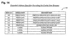
- an x86 ModR/M byte encodes the type of prefetch operation prescribed by a prefetch opcode 401 in bits 5:3 of the ModR/M byte.
- the x86 prefetch instruction allows values 000, 001, 010, and 011 to prescribe prefetch hints that are intended for read operations. All four values 000-011 direct an x86 microprocessor to prefetch data into its caches with varying degrees of closeness.
- a T0 hint (i.e., value 001)
- an NTA hint directs the microprocessor to prefetch a cache line into a non-temporal cache structure and into a location close to the processor, while minimizing cache pollution.
- the common feature of the x86 prefetch hints encoded as 000-011 is that a data read request is issued over the bus that requests a copy of a cache line regardless of its MESI state.
- One embodiment of the present invention encodes an additional hint in the extended address specifier that directs a microprocessor according to the present invention to prefetch a prescribed cache line using an exclusive (.S) hint.
- S exclusive
- FIGURE 5 shows the prefetch-exclusive hint encoding as value 100 in bits 5:3 of an x86 ModR/M byte.
- a conforming microprocessor is directed to issue transactions over a memory bus to prefetch data in the exclusive MESI state.
- the specific transaction that is issued responsive to a prefetch.s hint in the prefetch instruction 400 is a data read-and-invalidate transaction, such as has been previously described with reference to FIGURE 3B. In that example, the data read-and-invalidate transaction was required to raise the state of a shared cache line to the exclusive state.
- the extended prefetch instruction 400 can only request that prefetching be performed according to the hints provided. If a cache is not presently occupied with memory accesses, then prefetch operations are executed. But if a cache is otherwise busy, prefetch operations are deferred until the memory accesses are completed.
- FIGURE 6 a block diagram is presented detailing a microprocessor 600 according to the present invention for performing a prefetch-with-intent-to-store operation.
- the microprocessor 600 has three notable stage categories: fetch, translate, and execute.
- the fetch stage has fetch logic 601 that retrieves macro instructions into an instruction cache 602 from an instruction memory 603. The retrieved macro instructions are provided to the translate stage via an instruction queue 604.
- the translate stage has translation logic 606 that is coupled to a micro instruction queue 608.
- the translation logic 606 includes extended translation logic 607.
- the execute stage has execution logic 609 that includes an extended cache unit 610.
- the extended cache unit 610 has a data cache 611, that is coupled to extended fill logic 612.
- the extended fill logic 612 is coupled to a bus unit 613.
- the bus unit 613 is coupled to a data memory 614.
- the fetch logic 601 retrieves formatted instructions according to the present invention into the instruction cache 602 from the instruction memory 603, and provides the macro instructions in the instruction queue 604 in execution order.
- the macro instructions are retrieved from the instruction queue 604 and are provided to the translation logic 606.
- the translation logic 606 translates each of the provided macro instructions into a corresponding micro instruction sequence that directs the microprocessor 600 to perform the operations prescribed by the macro instructions.
- the extended translation logic 607 detects extended prefetch macro instructions according to the present invention and also provides for translation of corresponding extended prefixes and address specifier entities.
- the extended translation logic 607 is configured to detect an x86 prefetch instruction and to translate the ModR/M byte of the x86 prefetch instruction according to the conventions described with reference to FIGURES 4-5 into a prefetch micro instruction sequence directing the microprocessor 600 to exclusively prefetch a cache line into data cache 611.
- the micro instructions are routed from the micro instruction queue 608 to the execution logic 609, wherein the extended cache unit 610 is configured to execute an exclusive prefetch operation according to the present invention.
- the extended fill logic 612 directs the bus unit 613 to issue transactions over a memory bus 615 to the data memory 614 requesting that a prescribed cache line be prefetched into the data cache 611 in the exclusive MESI state.
- microprocessor 600 described with reference to FIGURE 6 is a simplified representation of a pipeline microprocessor 600 according to the present invention.
- today's pipeline microprocessor architectures comprise many pipeline stages.
- these stages can be generally categorized into the three stage groups shown in the block diagram and thus, the block diagram of FIGURE 6 serves to teach the essential elements that are required to implement embodiments of the present invention as described hereinabove.
- Those elements of a microprocessor 600 which are extraneous to the present discussion, for clarity, are not depicted.
- an extended prefetch instruction 702, PREFETCH.S [EAX] in the exemplary flow directs the microprocessor 701 to exclusively prefetch the cache line whose address corresponds to the contents of register EAX.
- a second macro instruction 702, MOV EBX, [EAX] directs the microprocessor 701 to read the contents of a memory location whose address is prescribed by register EAX and write the contents in register EBX.
- a third macro instruction, INC EBX directs the microprocessor 701 to increment the contents of register EBX.
- a fourth macro instruction, MOV [EAX],EBX directs the microprocessor 701 to store the contents of register EBX in a memory location corresponding to the contents of register EAX.
- one of the bus agents 741 has a local copy of the requested line in the exclusive state, then according to the specific bus transaction protocol that is employed, it snoops the transaction on the bus 740 requesting the line and invalidates its local copy. If the local copy has been modified, then the bus agent writes the modified data out to the bus 740 allowing the microprocessor 701 to obtain exclusive ownership of the line. If more than one bus agent 741 shares the line, then they all invalidate their local copies so that the line is provided to the microprocessor 701 in the exclusive state. In either of the cases, the requested line is provided to the cache 722 in the exclusive state and is available for a subsequent store operation.
- the translator 710 translates the second macro instruction 702 into a load micro instruction 711, LD EBX,[EAX], directing the microprocessor to load the contents the memory address prescribed by register EAX into register EBX. Because the cache line containing the contents is already resident in the data cache 722 as a result of the prefetch-with-intent-to-store operation, it is immediately available and the load micro instruction 711 is executed without delay.
- the third macro instruction 702 is translated into a corresponding increment micro instruction 711, INC EBX, that directs execute logic to increment the contents of register EBX. Since no new data is required, the load micro instruction 711 is not provided to the extended cache unit 720.
- the fourth macro instruction 702 in the flow is translated into a store micro instruction 711, ST [EAX],EBX, that directs the execute logic to perform a data store operation to write the contents of register EBX into the memory location addressed by the contents of register EAX.
- the store micro instruction 711 is thus provided to the extended cache unit 720 as a pending store operation. Accordingly, the fill logic 721 detects that the cache line targeted for the pending store operation is present in the data cache 222 and as a result of the exclusive prefetch, the cache line is in the exclusive state. Consequently, the store can be posted without delay.
- the extended cache unit 720 according to the present invention need not assert a stall signal 723 to post the pending store because the target cache line was exclusively prefetched.
- a timing diagram 800 is presented illustrating bus transactions 801, 802 that are issued over a memory bus 740 by the microprocessor of FIGURES 6 and 7 to perform the prefetch-with-intent-to-store operation according to the present invention.
- the transactions 801, 802 include request transactions 801 from the bus unit 730 to the memory bus 740 and response transactions 802 from the memory bus 740 back to the bus unit 730 within the microprocessor 701.
- the timing diagram 800 depicts those transactions 801, 802 that are conducted when a cache line is requested and provided exclusively as a response to a prefetch-with-intent-to-store operation that is prescribed by a prefetch-exclusive macro instruction according to the present invention.
- the extended fill logic 721 directs the bus unit 730 to issue a data read-and-invalidate request 801, DATA READ/INV [EAX], to the memory bus 740 requesting that the cache line prescribed by register EAX be provided to the local cache 722 in the exclusive MESI state.
- the data read-and-invalidate request 801 is issued at time A.
- the memory bus 740 sends a data response 802, DATA RESP [EAX].E, back to the bus unit 230 at time B providing the requested cache line in the exclusive MESI state.
- the data can be read from cache 222 or written to by a store operation without incurring bus transaction delay.
- FIGURE 9 is a block diagram showing an extended block prefetch instruction 900 according to the present invention.
- the extended block prefetch instruction 900 includes an optional plurality of prefix entities 901, one of which is a repeat prefix 901.
- the prefix entities 901 are followed by a prefetch opcode 902, which is followed by an extended address specifier 903.
- each of prefix and extended address entities 901, 903 are 8-bits in size
- the prefetch opcode entity 902 is one or two bytes in size and all entities 901-903 conform to the x86 instruction set architecture except as modified herein.
- the x86 repeat prefix (REP) 901 is employed to indicate a block prefetch operation.
- REP x86 repeat prefix
- the prefetch opcode 902 is a specific opcode value that directs a conforming microprocessor to perform a prefetch operation.
- the specify value of the opcode entity 901 is OF18h.
- the extended address specifier 903 is employed to specify the specific type of prefetch operation that is to be executed.
- the extended address specifier 903 is the ModR/M byte 903.
- a prefetch macro instruction 900 when detected by a microprocessor according to the present invention, the microprocessor is directed to prefetch data into cache from memory according to hint values as specified by contents of the extended address specifier 903.
- the encoding example described with reference to FIGURE 5 describes encoding of prefix hints in the block extended address specifier 903 as well.
- the microprocessor detects a repeat prefix 901 within the extended prefetch instruction 900, then the microprocessor attempts to prefetch a specified number of cache lines into its local cache in the exclusive state, where the number of cache lines is prescribed in an architectural register within the microprocessor. In one embodiment, the number of cache lines is specified within register ECX in an x86-compatible microprocessor.
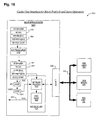
- a block diagram 1000 is presented depicting a cache unit interface to memory for performing a block prefetch and store operation within the microprocessor 600 of FIGURE 6.
- Identification and operation of the elements within the microprocessor 1001 of FIGURE 10 are similar to those like elements within the microprocessor 701 of FIGURE 7, where the hundreds digit is replaced by a 10.
- an extended translator 1010 is enabled to translate an extended prefetch instruction with a repeat prefix 1002 into a micro instruction sequence 1011 directing an exclusive block prefetch operation.
- a shadow count register 1013 is provided to which the number of cache lines to be prefetched is loaded from an architectural register 1012.
- extended block fill logic 1021 is provided to direct the bus unit 1030 to request exclusive prefetch of the specified block of cache lines, and to provide those lines into the data cache 1022 upon receipt.
- a first macro instruction 1002, MOV ECX,COUNT is provided to initialize architectural register ECX with the number of cache lines in the block that are to be prefetched exclusively.
- the extended translator 1010 translates the first macro instruction into a load micro instruction 1011, LD ECX,COUNT, directing the microprocessor to load the count into ECX.
- the count is loaded into ECX, it is also transparently copied into the shadow count register 1013, SHECX.
- other instructions 1002 may modify the architectural register 1012 without disturbing the count for the prefetch operation.
- an extended block prefetch instruction 1002, REP.PREF.S [EAX] is translated by the extended translator 1010 that directs the microprocessor 1001 to prefetch the number of cache lines prescribed by ECX into local cache in the exclusive state, where the address of the first cache line to be prefetched is prescribed in register EAX.
- the extended block fill logic 1021 directs the bus unit 1030 to issue bus requests over the memory bus 1040 requesting the cache lines beginning at the address prescribed by EAX in the exclusive state.
- the fill logic 1021 receives these lines as they arrive and allocates them into the data cache 1022. Once entered into the cache in the exclusive state, any or all of the prefetched cache lines may be modified without incurring additional delay.
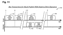
- FIGURE 11 a timing diagram 1100 is presented illustrating bus transactions 1101, 1102 that are issued over a memory bus 1040 by the microprocessor 1001 of FIGURES 6 and 10 to perform the block prefetch and store operation according to the present invention.
- the example of FIGURE 11 presumes 32-byte cache lines in a system configuration.
- the transactions 1101, 1102 include request transactions 1101 from the bus unit 1030 to the memory bus 1040 and response transactions 1102 from the memory bus 1040 back to the bus unit 1030 within the microprocessor 1001.
- the timing diagram 1000 depicts those transactions 1001, 1002 that are conducted when a block of cache lines is requested and provided exclusively as a response to a block prefetch-with-intent-to-store operation that is prescribed by a prefetch-exclusive macro instruction according to the present invention that includes a repeat prefix.
- the extended fill logic 1021 directs the bus unit 1030 to issue a plurality of data read-and-invalidate requests 1101 that correspond to the number of cache lines specified within the architectural register.
- the plurality of requests includes the addresses of the all of the cache lines in the cache line block, as initially specified by contents of an architectural register, EAX.
- bus requests 1101 are provided in ascending address order, it is noted that the present invention comprehends descending order, random ordering, and staggered ordering to accommodate the conventions of different memory bus protocols.
- a first data read-and-invalidate request 1101 is issued at time A, a second request 1101 at time B, and so on until a final request 1101 is provided at time D.
- bus responses 1102 are tagged and consequently, they may begin to arrive at time C prior to completion of the last request.
- time C At time C, at least one cache line in the block is available for a pending store. However, to ensure that delay is minimized, it is recommended that store operations to the block of lines be postponed until time E, when all of the responses 1102 have been received in the exclusive state.
- the memory bus 1040 sends a data response 802, DATA RESP [EAX].E, back to the bus unit 1030 at time B providing the requested cache line in the exclusive MESI state.
- the data can be read from cache 1022 or written to by a store operation without incurring bus transaction delay.
- a subsequent write transaction 1101, DATA WRITE [EAX] may be executed without delay as a result of a subsequent store operation because the block of cache lines was exclusively obtained.
- the data write transaction 1101 does not result from execution of the exclusive block prefetch instruction.
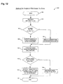
- FIGURE 12 a flow chart 1200 is presented illustrating a method according to the present invention for performing a prefetch-with-intent-to-store operation.
- Flow begins at block 1202 where a flow of macro instructions is provided to an instruction queue according to the present invention. Flow then proceeds to block 1204.
- a next macro instruction is fetched from the instruction queue and provided to an extended translator. Flow then proceeds to decision block 1206.
- an evaluation is made to determine if the next macro instruction is an extended prefetch instruction. If so, then flow is directed to block 1208. If not, then flow proceeds to block 1210.
- a detected extended prefetch instruction is translated into a prefetch-with-intent-to-store micro instruction sequence that directs a microprocessor to prefetch a specified cache line in the exclusive state. Flow then proceeds to block 1212.
- the macro instruction is translated into a corresponding micro instruction sequence directing the microprocessor to perform a specified operation. Flow then proceeds to block 1212.
- a next micro instruction sequence is provided to execute logic in the microprocessor. Flow then proceeds to decision block 1214.
- next micro instruction sequence is evaluated to determine if it is a prefetch-with-intent-to-store sequence. If so, then flow is directed toward block 1216. If not, then flow proceeds to block 1218.
- bus transactions are issued to a memory bus requesting exclusive ownership of a prescribed cache line.
- the cache line is provided to the microprocessor in the exclusive MESI state and is thus available for store operations without incurring bus delay to raise the state of the line so that it can be modified. Flow is then directed to block 1220.
- FIGURE 13 a flow chart 1300 is presented illustrating a method according to the present invention for performing a block prefetch-with-intent-to-store operation.
- Flow begins at block 1302 where a flow of macro instructions is provided to an instruction queue according to the present invention. Flow then proceeds to block 1304.
- a next macro instruction is fetched from the instruction queue and provided to an extended translator. Flow then proceeds to decision block 1306.
- an evaluation is made to determine if the next macro instruction is an extended block prefetch instruction. If so, then flow is directed to block 1310. If not, then flow proceeds to block 1308.
- a temporary counter is initialized to zero to monitor the number of bus transactions that will be issued requesting exclusive ownership of a block of cache lines. Flow then proceeds to block 1320.
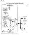
- FIGURE 15 a block diagram 1500 is presented depicting a cache unit interface to memory for performing an allocate and rename operation within the microprocessor of FIGURE 6.
- a rename operation on an exclusively fetched cache line is executed, responsive to an allocate and rename instruction encoded as described with reference to FIGURE 14.
- the block diagram 1500 shows logic within the microprocessor 1501 that is employed to perform the allocate and rename operation.
- the microprocessor 1501 has an extended translator 1510 that receives a flow of macro instructions 1502 and translates the macro instructions 1502 into associated micro instructions 1511.
- Micro instructions 1500 that direct data load and store operations from and to memory 1542 are subsequently provided to an extended cache unit 1520.
- the extended cache unit 1520 includes extended cache logic 1521 and a data cache 1522.
- the extended cache logic 1521 is coupled to a bus unit 1530.
- the bus unit 1530 interfaces to a system memory bus 1540, to which the data memory 1542 and other bus agents 1541 are coupled.
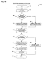
- the macro instruction is translated into a corresponding micro instruction sequence directing the microprocessor to perform a specified operation. Flow then proceeds to block 1612.
- a next micro instruction sequence is provided to execute logic in the microprocessor. Flow then proceeds to decision block 1814.
- a data read-and-invalidate transaction is issued over the memory bus to allocate the first cache line at DSTADDR in the exclusive MESI state. Flow then proceeds to block 1824.
- an evaluation is made to determine is the incremented count is equal to the number of cache lines to be allocated and renamed, as stored in a shadow register to which the count was copied. If not, flow proceeds to block 1820, where another iteration is executed to allocate and rename a next destination cache line. If the count equals the contents of the shadow register, then all allocate and rename operations have been completed for the block of cache lines and flow is directed to block 1830.
- the present invention has been characterized herein as providing advantages for pending store operations or eliminating store operations altogether in accordance with the MESI protocol.
- MESI has been selected to exemplify the present invention because of its prevalent use in the art.
- the present invention provides for prefetching of data into a local cache in such a form, or state, that it can be immediately modified without a need to issues transactions to a memory bus. Whether that form or state accords with MESI is inconsequential.
- cache line width varies according to architecture. In desktop systems, 32-byte cache lines prevail today. But such representation of the present invention is not intended to restrict its application to 32-, 64-, 128-, or even 256-byte cache lines. On the contrary, it is contemplated that the present invention is applicable to any system architecture that restricts modification of local cache lines and which does not provide for direct prefetch of those lines so that they can be immediately modified without resorting to bus transactions to obtain permission to do so.
- an address specifier is employed herein to specify an address of a cache line to be allocated and renamed, such specification need not be explicit.
- An embodiment of an allocate and rename instruction according to the present invention could implicitly specify an architectural register that contains the address, where a prior instruction is executed to load the address into the architectural register.
Landscapes
- Engineering & Computer Science (AREA)
- Theoretical Computer Science (AREA)
- Software Systems (AREA)
- Physics & Mathematics (AREA)
- General Engineering & Computer Science (AREA)
- General Physics & Mathematics (AREA)
- Memory System Of A Hierarchy Structure (AREA)
Applications Claiming Priority (4)
| Application Number | Priority Date | Filing Date | Title |
|---|---|---|---|
| US405980 | 2003-04-02 | ||
| US10/405,980 US7111125B2 (en) | 2002-04-02 | 2003-04-02 | Apparatus and method for renaming a data block within a cache |
| US10/464,353 US7188215B2 (en) | 2003-06-19 | 2003-06-19 | Apparatus and method for renaming a cache line |
| US464353 | 2003-06-19 |
Publications (3)
| Publication Number | Publication Date |
|---|---|
| EP1465059A2 true EP1465059A2 (de) | 2004-10-06 |
| EP1465059A3 EP1465059A3 (de) | 2007-12-05 |
| EP1465059B1 EP1465059B1 (de) | 2018-05-09 |
Family
ID=32853160
Family Applications (1)
| Application Number | Title | Priority Date | Filing Date |
|---|---|---|---|
| EP03257877.5A Expired - Lifetime EP1465059B1 (de) | 2003-04-02 | 2003-12-15 | Vorrichtung und Verfahren zum Umbenennen einer Cachespeicherzeile |
Country Status (1)
| Country | Link |
|---|---|
| EP (1) | EP1465059B1 (de) |
Citations (1)
| Publication number | Priority date | Publication date | Assignee | Title |
|---|---|---|---|---|
| EP0375883A2 (de) | 1988-12-30 | 1990-07-04 | International Business Machines Corporation | Cache-Speicheranordnung |
Family Cites Families (1)
| Publication number | Priority date | Publication date | Assignee | Title |
|---|---|---|---|---|
| US6842830B2 (en) * | 2001-03-31 | 2005-01-11 | Intel Corporation | Mechanism for handling explicit writeback in a cache coherent multi-node architecture |
-
2003
- 2003-12-15 EP EP03257877.5A patent/EP1465059B1/de not_active Expired - Lifetime
Patent Citations (1)
| Publication number | Priority date | Publication date | Assignee | Title |
|---|---|---|---|---|
| EP0375883A2 (de) | 1988-12-30 | 1990-07-04 | International Business Machines Corporation | Cache-Speicheranordnung |
Non-Patent Citations (1)
| Title |
|---|
| TULLSEN D M; EGGERS S J, ACM TRANSACTIONS ON COMPUTER SYSTEMS, vol. 13, 1995, pages 57 - 88 |
Also Published As
| Publication number | Publication date |
|---|---|
| EP1465059B1 (de) | 2018-05-09 |
| EP1465059A3 (de) | 2007-12-05 |
Similar Documents
| Publication | Publication Date | Title |
|---|---|---|
| US7111125B2 (en) | Apparatus and method for renaming a data block within a cache | |
| EP1447741B1 (de) | Mechanismus zur Zuweisung und Initialisierung von Cachedatenblöcken | |
| US7000081B2 (en) | Write back and invalidate mechanism for multiple cache lines | |
| US7188215B2 (en) | Apparatus and method for renaming a cache line | |
| US8930635B2 (en) | Page invalidation processing with setting of storage key to predefined value | |
| US8521964B2 (en) | Reducing interprocessor communications pursuant to updating of a storage key | |
| US8918601B2 (en) | Deferred page clearing in a multiprocessor computer system | |
| US10102124B2 (en) | High bandwidth full-block write commands | |
| EP1447744B1 (de) | Exklusive Vorausladung eines Datenblocks aus einem Speicher | |
| EP1447743B1 (de) | Anordnung und Verfahren zur Zuteilung und Initialisierung einer Cachespeicherzeile | |
| EP1447745B1 (de) | Vorausladungsmechanismus mit Speicherabsicht | |
| US20100306475A1 (en) | Data cache with modified bit array | |
| EP1465059B1 (de) | Vorrichtung und Verfahren zum Umbenennen einer Cachespeicherzeile | |
| TWI782754B (zh) | 微處理器和在微處理器中實現的方法 | |
| IE901526A1 (en) | Method and apparatus for increasing the data storage rate of¹a computer system having a predefined data path width |
Legal Events
| Date | Code | Title | Description |
|---|---|---|---|
| PUAI | Public reference made under article 153(3) epc to a published international application that has entered the european phase |
Free format text: ORIGINAL CODE: 0009012 |
|
| AK | Designated contracting states |
Kind code of ref document: A2 Designated state(s): AT BE BG CH CY CZ DE DK EE ES FI FR GB GR HU IE IT LI LU MC NL PT RO SE SI SK TR |
|
| AX | Request for extension of the european patent |
Extension state: AL LT LV MK |
|
| PUAL | Search report despatched |
Free format text: ORIGINAL CODE: 0009013 |
|
| AK | Designated contracting states |
Kind code of ref document: A3 Designated state(s): AT BE BG CH CY CZ DE DK EE ES FI FR GB GR HU IE IT LI LU MC NL PT RO SE SI SK TR |
|
| AX | Request for extension of the european patent |
Extension state: AL LT LV MK |
|
| 17P | Request for examination filed |
Effective date: 20080128 |
|
| 17Q | First examination report despatched |
Effective date: 20080627 |
|
| AKX | Designation fees paid |
Designated state(s): DE GB |
|
| RAP1 | Party data changed (applicant data changed or rights of an application transferred) |
Owner name: IP-FIRST, LLC. |
|
| STAA | Information on the status of an ep patent application or granted ep patent |
Free format text: STATUS: EXAMINATION IS IN PROGRESS |
|
| GRAP | Despatch of communication of intention to grant a patent |
Free format text: ORIGINAL CODE: EPIDOSNIGR1 |
|
| STAA | Information on the status of an ep patent application or granted ep patent |
Free format text: STATUS: GRANT OF PATENT IS INTENDED |
|
| INTG | Intention to grant announced |
Effective date: 20180301 |
|
| GRAS | Grant fee paid |
Free format text: ORIGINAL CODE: EPIDOSNIGR3 |
|
| GRAA | (expected) grant |
Free format text: ORIGINAL CODE: 0009210 |
|
| STAA | Information on the status of an ep patent application or granted ep patent |
Free format text: STATUS: THE PATENT HAS BEEN GRANTED |
|
| AK | Designated contracting states |
Kind code of ref document: B1 Designated state(s): DE GB |
|
| REG | Reference to a national code |
Ref country code: GB Ref legal event code: FG4D |
|
| REG | Reference to a national code |
Ref country code: DE Ref legal event code: R096 Ref document number: 60351180 Country of ref document: DE |
|
| REG | Reference to a national code |
Ref country code: DE Ref legal event code: R096 Ref document number: 60351180 Country of ref document: DE |
|
| REG | Reference to a national code |
Ref country code: DE Ref legal event code: R097 Ref document number: 60351180 Country of ref document: DE |
|
| PLBE | No opposition filed within time limit |
Free format text: ORIGINAL CODE: 0009261 |
|
| STAA | Information on the status of an ep patent application or granted ep patent |
Free format text: STATUS: NO OPPOSITION FILED WITHIN TIME LIMIT |
|
| 26N | No opposition filed |
Effective date: 20190212 |
|
| REG | Reference to a national code |
Ref country code: DE Ref legal event code: R082 Ref document number: 60351180 Country of ref document: DE Representative=s name: HL KEMPNER PATENTANWAELTE, SOLICITORS (ENGLAND, DE Ref country code: DE Ref legal event code: R082 Ref document number: 60351180 Country of ref document: DE Representative=s name: HL KEMPNER PATENTANWALT, RECHTSANWALT, SOLICIT, DE |
|
| PGFP | Annual fee paid to national office [announced via postgrant information from national office to epo] |
Ref country code: GB Payment date: 20221128 Year of fee payment: 20 Ref country code: DE Payment date: 20220603 Year of fee payment: 20 |
|
| REG | Reference to a national code |
Ref country code: DE Ref legal event code: R071 Ref document number: 60351180 Country of ref document: DE |
|
| REG | Reference to a national code |
Ref country code: GB Ref legal event code: PE20 Expiry date: 20231214 |
|
| PG25 | Lapsed in a contracting state [announced via postgrant information from national office to epo] |
Ref country code: GB Free format text: LAPSE BECAUSE OF EXPIRATION OF PROTECTION Effective date: 20231214 |
|
| PG25 | Lapsed in a contracting state [announced via postgrant information from national office to epo] |
Ref country code: GB Free format text: LAPSE BECAUSE OF EXPIRATION OF PROTECTION Effective date: 20231214 |