EP1465148A1 - Bildanzeigevorrichtung, Steuerverfahren dafür und elektronisches Gerät - Google Patents
Bildanzeigevorrichtung, Steuerverfahren dafür und elektronisches Gerät Download PDFInfo
- Publication number
- EP1465148A1 EP1465148A1 EP04016265A EP04016265A EP1465148A1 EP 1465148 A1 EP1465148 A1 EP 1465148A1 EP 04016265 A EP04016265 A EP 04016265A EP 04016265 A EP04016265 A EP 04016265A EP 1465148 A1 EP1465148 A1 EP 1465148A1
- Authority
- EP
- European Patent Office
- Prior art keywords
- electrode
- signal
- voltage
- pixel
- electrodes
- Prior art date
- Legal status (The legal status is an assumption and is not a legal conclusion. Google has not performed a legal analysis and makes no representation as to the accuracy of the status listed.)
- Granted
Links
- 238000000034 method Methods 0.000 title description 18
- 239000004973 liquid crystal related substance Substances 0.000 description 97
- 238000010586 diagram Methods 0.000 description 12
- 239000000758 substrate Substances 0.000 description 8
- 239000011159 matrix material Substances 0.000 description 6
- 230000003247 decreasing effect Effects 0.000 description 5
- 239000011521 glass Substances 0.000 description 4
- 238000007789 sealing Methods 0.000 description 3
- 238000002834 transmittance Methods 0.000 description 3
- 239000004020 conductor Substances 0.000 description 1
- 230000001419 dependent effect Effects 0.000 description 1
- 230000000694 effects Effects 0.000 description 1
- 238000012986 modification Methods 0.000 description 1
- 230000004048 modification Effects 0.000 description 1
- 239000010409 thin film Substances 0.000 description 1
Images






Classifications
-
- G—PHYSICS
- G09—EDUCATION; CRYPTOGRAPHY; DISPLAY; ADVERTISING; SEALS
- G09G—ARRANGEMENTS OR CIRCUITS FOR CONTROL OF INDICATING DEVICES USING STATIC MEANS TO PRESENT VARIABLE INFORMATION
- G09G3/00—Control arrangements or circuits, of interest only in connection with visual indicators other than cathode-ray tubes
- G09G3/20—Control arrangements or circuits, of interest only in connection with visual indicators other than cathode-ray tubes for presentation of an assembly of a number of characters, e.g. a page, by composing the assembly by combination of individual elements arranged in a matrix no fixed position being assigned to or needed to be assigned to the individual characters or partial characters
- G09G3/34—Control arrangements or circuits, of interest only in connection with visual indicators other than cathode-ray tubes for presentation of an assembly of a number of characters, e.g. a page, by composing the assembly by combination of individual elements arranged in a matrix no fixed position being assigned to or needed to be assigned to the individual characters or partial characters by control of light from an independent source
- G09G3/36—Control arrangements or circuits, of interest only in connection with visual indicators other than cathode-ray tubes for presentation of an assembly of a number of characters, e.g. a page, by composing the assembly by combination of individual elements arranged in a matrix no fixed position being assigned to or needed to be assigned to the individual characters or partial characters by control of light from an independent source using liquid crystals
-
- G—PHYSICS
- G09—EDUCATION; CRYPTOGRAPHY; DISPLAY; ADVERTISING; SEALS
- G09G—ARRANGEMENTS OR CIRCUITS FOR CONTROL OF INDICATING DEVICES USING STATIC MEANS TO PRESENT VARIABLE INFORMATION
- G09G3/00—Control arrangements or circuits, of interest only in connection with visual indicators other than cathode-ray tubes
- G09G3/20—Control arrangements or circuits, of interest only in connection with visual indicators other than cathode-ray tubes for presentation of an assembly of a number of characters, e.g. a page, by composing the assembly by combination of individual elements arranged in a matrix no fixed position being assigned to or needed to be assigned to the individual characters or partial characters
- G09G3/34—Control arrangements or circuits, of interest only in connection with visual indicators other than cathode-ray tubes for presentation of an assembly of a number of characters, e.g. a page, by composing the assembly by combination of individual elements arranged in a matrix no fixed position being assigned to or needed to be assigned to the individual characters or partial characters by control of light from an independent source
- G09G3/36—Control arrangements or circuits, of interest only in connection with visual indicators other than cathode-ray tubes for presentation of an assembly of a number of characters, e.g. a page, by composing the assembly by combination of individual elements arranged in a matrix no fixed position being assigned to or needed to be assigned to the individual characters or partial characters by control of light from an independent source using liquid crystals
- G09G3/3611—Control of matrices with row and column drivers
- G09G3/3648—Control of matrices with row and column drivers using an active matrix
- G09G3/3659—Control of matrices with row and column drivers using an active matrix the addressing of the pixel involving the control of two or more scan electrodes or two or more data electrodes, e.g. pixel voltage dependant on signal of two data electrodes
-
- G—PHYSICS
- G09—EDUCATION; CRYPTOGRAPHY; DISPLAY; ADVERTISING; SEALS
- G09G—ARRANGEMENTS OR CIRCUITS FOR CONTROL OF INDICATING DEVICES USING STATIC MEANS TO PRESENT VARIABLE INFORMATION
- G09G2300/00—Aspects of the constitution of display devices
- G09G2300/08—Active matrix structure, i.e. with use of active elements, inclusive of non-linear two terminal elements, in the pixels together with light emitting or modulating elements
- G09G2300/0809—Several active elements per pixel in active matrix panels
- G09G2300/0814—Several active elements per pixel in active matrix panels used for selection purposes, e.g. logical AND for partial update
-
- G—PHYSICS
- G09—EDUCATION; CRYPTOGRAPHY; DISPLAY; ADVERTISING; SEALS
- G09G—ARRANGEMENTS OR CIRCUITS FOR CONTROL OF INDICATING DEVICES USING STATIC MEANS TO PRESENT VARIABLE INFORMATION
- G09G2300/00—Aspects of the constitution of display devices
- G09G2300/08—Active matrix structure, i.e. with use of active elements, inclusive of non-linear two terminal elements, in the pixels together with light emitting or modulating elements
- G09G2300/0809—Several active elements per pixel in active matrix panels
- G09G2300/0842—Several active elements per pixel in active matrix panels forming a memory circuit, e.g. a dynamic memory with one capacitor
-
- G—PHYSICS
- G09—EDUCATION; CRYPTOGRAPHY; DISPLAY; ADVERTISING; SEALS
- G09G—ARRANGEMENTS OR CIRCUITS FOR CONTROL OF INDICATING DEVICES USING STATIC MEANS TO PRESENT VARIABLE INFORMATION
- G09G2310/00—Command of the display device
- G09G2310/02—Addressing, scanning or driving the display screen or processing steps related thereto
- G09G2310/0243—Details of the generation of driving signals
- G09G2310/0251—Precharge or discharge of pixel before applying new pixel voltage
-
- G—PHYSICS
- G09—EDUCATION; CRYPTOGRAPHY; DISPLAY; ADVERTISING; SEALS
- G09G—ARRANGEMENTS OR CIRCUITS FOR CONTROL OF INDICATING DEVICES USING STATIC MEANS TO PRESENT VARIABLE INFORMATION
- G09G2330/00—Aspects of power supply; Aspects of display protection and defect management
- G09G2330/02—Details of power systems and of start or stop of display operation
- G09G2330/021—Power management, e.g. power saving
-
- G—PHYSICS
- G09—EDUCATION; CRYPTOGRAPHY; DISPLAY; ADVERTISING; SEALS
- G09G—ARRANGEMENTS OR CIRCUITS FOR CONTROL OF INDICATING DEVICES USING STATIC MEANS TO PRESENT VARIABLE INFORMATION
- G09G2330/00—Aspects of power supply; Aspects of display protection and defect management
- G09G2330/02—Details of power systems and of start or stop of display operation
- G09G2330/021—Power management, e.g. power saving
- G09G2330/023—Power management, e.g. power saving using energy recovery or conservation
-
- G—PHYSICS
- G09—EDUCATION; CRYPTOGRAPHY; DISPLAY; ADVERTISING; SEALS
- G09G—ARRANGEMENTS OR CIRCUITS FOR CONTROL OF INDICATING DEVICES USING STATIC MEANS TO PRESENT VARIABLE INFORMATION
- G09G3/00—Control arrangements or circuits, of interest only in connection with visual indicators other than cathode-ray tubes
- G09G3/20—Control arrangements or circuits, of interest only in connection with visual indicators other than cathode-ray tubes for presentation of an assembly of a number of characters, e.g. a page, by composing the assembly by combination of individual elements arranged in a matrix no fixed position being assigned to or needed to be assigned to the individual characters or partial characters
- G09G3/34—Control arrangements or circuits, of interest only in connection with visual indicators other than cathode-ray tubes for presentation of an assembly of a number of characters, e.g. a page, by composing the assembly by combination of individual elements arranged in a matrix no fixed position being assigned to or needed to be assigned to the individual characters or partial characters by control of light from an independent source
- G09G3/36—Control arrangements or circuits, of interest only in connection with visual indicators other than cathode-ray tubes for presentation of an assembly of a number of characters, e.g. a page, by composing the assembly by combination of individual elements arranged in a matrix no fixed position being assigned to or needed to be assigned to the individual characters or partial characters by control of light from an independent source using liquid crystals
- G09G3/3611—Control of matrices with row and column drivers
- G09G3/3614—Control of polarity reversal in general
Definitions
- the present invention relates to a display device and an electronic equipment.
- a thin film transistor (hereinafter abbreviated as "TFT") liquid crystal device (display device in a broad sense) is mainly driven by using an alternating current (AC) drive method such as a frame inversion drive method, a line inversion drive method, and a dot inversion drive method.
- AC alternating current
- the dot inversion drive method is capable of effectively preventing occurrence of a flicker.
- a common electrode voltage Vcom a voltage Vp at which the voltage applied to the liquid crystal becomes positive, or a voltage Vm at which the voltage applied to the liquid crystal becomes negative is applied to a signal electrode according to AC drive timing, and written into a pixel capacitance (liquid crystal capacitance). This makes it necessary to drive the voltage to be applied to the signal electrode each time AC drive is performed, whereby power consumption is increased.
- EP-A-0 915 453 discloses a display device according to the pre-characterizing portion of claim 1.
- a scanning electrode of a first one of the two groups is selected to turn on only a p-channel type transistor (first pixel switch element) when a positive polarity image signal having a voltage higher than the common electrode potential is applied to a pixel electrode so that the signal may be written onto the pixel electrode from the corresponding signal electrode of a first one of the two groups of signal electrodes.
- a scanning electrode is selected to turn on only the n-channel type transistor (second pixel switch element) when a negative polarity image signal having a voltage lower than the middle potential is applied to the pixel electrode so that the signal may be written onto the pixel electrode from the corresponding signal electrode of the second group of signal electrodes.
- EP-A-1 158 482 discloses a display device having 3m scanning lines that extend in an X (row) direction, and n data lines that extend in a Y (column) direction (m and n are integers). Three subpixels are respectively arranged at the intersections of the scanning lines and the data lines. Three subpixels adjacent to each other in the column direction are grouped as a single pixel. Pixels are arranged in a matrix of m rows by n columns. A first signal line and a second signal line are arranged every row along the scanning line while an auxiliary data line is arranged every column along the data line. The scanning lines, the first signal lines, and the second signal lines have spacings therebetween that are set to reflect an area ratio of the subpixels of approximately 1:2:4.
- This particular structure of the known display device allows switching as appropriate between a display using an area gray scale method and a display of multi-level gray scale having a number of gray scale levels greater than the number of gray scale levels defined by the number of split subpixels.
- EP-A-0 506 530 discloses a matrix display device with improved definition, associated with at least one control circuit.
- This display device comprises, at each intersection of rows and columns of a conductor matrix, two switching transistors in such a way that each row-column pair controls two diagonally opposite pixels cells. Furthermore the even columns are linked to a first control circuit supplied with a first voltage and the odd columns to a second control circuit supplied with an inverse voltage.
- the given intermediate voltage is determined as an intermediate value between the voltages of the kth or (M+k)th signal electrodes based on the voltages of the kth or (M+k)th signal electrodes, for example.
- the claimed structure enables charges stored in the pixels arranged in a line to be transferred simultaneously, whereby the voltages of the pixel electrodes can be uniformly set at the given intermediate voltage without an external current in a former period of the select period. This effect can be obtained without providing additional electrodes, whereby the configuration can be simple. Moreover, only driving a signal electrode from the intermediate voltage to either a positive or a negative voltage is necessary, and alternately driving a signal electrode between a positive and a negative voltage in AC drive is unnecessary. As a result, power consumption accompanied with AC drive can be decreased.
- FIG. 1 shows an outline of a configuration of a liquid crystal device.
- a liquid crystal device (electro-optical device or display device in a broad sense) 10 is a TFT liquid crystal device.
- the liquid crystal device 10 includes a liquid crystal panel (display panel in a broad sense) 20.
- the liquid crystal panel 20 is formed on a glass substrate, for example.
- a plurality of first to Nth (N is an integer of two or more) scan electrodes (gate lines) G 1 to G N which are arranged in the Y direction and extend in the X direction, and a plurality of first to Mth (M is an integer of two or more) signal electrodes (source lines) S 1 to S M which are arranged in the X direction and extend in the Y direction are disposed on the glass substrate.
- Pixels (pixel regions) are disposed in the shape of a matrix corresponding to intersecting points of the first to Nth scan electrodes G 1 to G N and the first to Mth signal electrodes S 1 to S M .
- Each pixel includes a TFT as a pixel switch element, and a pixel electrode.
- the pixel corresponding to the intersecting point of the jth (1 ⁇ j ⁇ N, j is an integer) scan electrode G j and the kth (1 ⁇ k ⁇ M, k is an integer) signal electrode S k includes a TFT of which a gate electrode is connected with the jth scan electrode G j and a source terminal is connected with the kth signal electrode S k , and a pixel electrode of a liquid crystal (liquid crystal capacitance or pixel capacitance) (liquid crystal element in a broad sense) which is connected with a drain terminal of the TFT.
- liquid crystal liquid crystal capacitance or pixel capacitance
- the liquid crystal capacitance is formed by sealing a liquid crystal between the pixel electrode and a common electrode opposite to the pixel electrode.
- the transmittance of the pixel is changed corresponding to voltage applied between these electrodes.
- a common electrode voltage Vcom is supplied to the common electrode.
- the liquid crystal device 10 includes a signal driver (signal electrode driver circuit in a broad sense) 30.
- the signal driver 30 drives the first to Mth signal electrodes S 1 to S M of the liquid crystal panel 20 based on image data.
- the liquid crystal device 10 includes a scan driver 40.
- the scan driver 40 sequentially drives the first to Nth scan electrodes G 1 to G N of the liquid crystal panel 20 within one vertical scanning period.
- AC drive is performed by using a dot inversion drive method in order to prevent a DC component from being continuously applied to the liquid crystal of each pixel and effectively prevent occurrence of a flicker.
- the signal electrode is driven so that the polarity of the voltage applied to the liquid crystal is reversed by changing the voltage of the pixel electrode with respect to the common electrode voltage Vcom applied to the common electrode.
- FIGS. 2A and 2B are views for describing the dot inversion drive method.
- the polarity of the voltage applied to the liquid crystal is alternately reversed for each pixel in a frame unit.
- the pixels in which the polarity of the voltage applied to the liquid crystal is positive are indicated by "+”, and the pixels in which the polarity of the voltage applied to the liquid crystal is negative are indicated by "-”.
- the polarity of the voltage is reversed for each pixel between a frame f 1 and a subsequent frame f 2 , as shown in FIG. 2A.
- the voltage of the signal electrode of the pixel is changed as shown in FIG. 2B.
- a voltage Vp is supplied to the signal electrode of the pixel so that the polarity of the voltage applied to the liquid crystal becomes positive in the frame f 1
- the voltage of the signal electrode reaches the voltage Vp at a time t a1 in one horizontal scanning period (select period) along a charge characteristic curve C a1 .
- a liquid crystal device capable of decreasing power consumption accompanied by AC drive is provided by changing the configuration of the pixel.
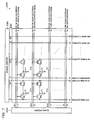
- FIG. 3 shows an outline of a configuration of a liquid crystal device in an example.
- a liquid crystal device 100 in the example may include a liquid crystal panel (display panel in a broad sense) 120.
- the liquid crystal panel 120 is formed on a glass substrate, for example.
- a plurality of first to Nth scan electrodes G 1 to G N which are arranged in the Y direction and extend in the X direction, and a plurality of first to Mth signal electrodes S 1 to S M which are arranged in the X direction and extend in the Y direction are disposed on the glass substrate.
- First to Mth electrodes SS 1 to SS M are disposed corresponding to the first to Mth signal electrodes S 1 to S M .
- the voltage Vp at which the voltage applied to the liquid crystal of the pixel becomes positive with respect to the common electrode voltage Vcom is supplied to the jth signal electrode S j among the first to Mth signal electrodes S 1 to S M .
- the common electrode voltage Vcom is supplied to the first to Mth electrodes SS 1 to SS M .
- (N+1)th to 2Nth scan electrodes GX 1 to GX N are disposed corresponding to each of the first to Nth scan electrodes G 1 to G N so as to be parallel to the first to Nth scan electrodes G 1 to G N , for example.
- (2N+1 )th to 3Nth scan electrodes GV 1 to GV N are disposed corresponding to each of the first to Nth scan electrodes G 1 to G N so as to be parallel to the first to Nth scan electrodes G 1 to G N , for example.
- Pixels are disposed in the shape of a matrix corresponding to the intersecting points of the first to Nth scan electrodes G 1 to G N and the first to Mth signal electrodes S 1 to S M .
- the pixel corresponding to the intersecting point of the jth scan electrode G j and the kth signal electrode S k is indicated by P jk .
- P 11 , P 12 , P 21 , and P 22 are illustrated in FIG. 3, other pixels have the same configuration.
- the liquid crystal device 100 may include a signal driver 130.
- the common electrode voltage Vcom may be applied to the first to Mth electrodes SS 1 to SS M from either the signal driver 130 or a power supply circuit (not shown).
- the liquid crystal device 100 may include a scan driver 140.
- a circuit functionally equivalent to the signal driver 130 may be formed on the substrate on which the liquid crystal panel 120 is formed.
- a circuit functionally equivalent to the scan driver 140 may be formed on the substrate.
- FIG. 4 is a configuration diagram of the pixels of the liquid crystal device in the example.
- pixels P jk , P j(k+1) , P (j+1)k , and P (j+1)(k+1) are illustrated.
- the pixel P jk includes a first pixel switch element SW jk and a pixel electrode E jk .
- a gate electrode of the first pixel switch element SW jk is connected with the jth scan electrode G j .
- a source terminal of the first pixel switch element SW jk is connected with the kth signal electrode S k .
- a drain terminal of the first pixel switch element SW jk is connected with the pixel electrode E jk .
- the first pixel switch element SW jk electrically connects the kth signal electrode S k with the pixel electrode E jk based on the voltage of the jth scan electrode G j .
- the first pixel switch element SW jk may be realized by using a TFT.
- the pixel P jk may include a second pixel switch element XSW jk .
- a drain terminal of the second pixel switch element XSW jk is connected with the pixel electrode E jk .
- the second pixel switch element XSW jk may be realized by using a TFT.
- the pixel P jk may include a switch element VSW jk .
- a source terminal of the switch element VSW jk is connected with the kth electrode SS k .
- a drain terminal of the switch element VSW jk is connected with the pixel electrode E jk .
- the switch element VSW jk may be realized by using a TFT.
- a liquid crystal capacitance is formed by sealing a liquid crystal between the pixel electrode E jk and the common electrode opposite to the pixel electrode E jk .
- the transmittance of the pixel is changed corresponding to the voltage applied between these electrodes.
- the common electrode voltage Vcom is supplied to the common electrode.
- the voltage of the pixel electrode E jk is set at the common electrode voltage Vcom.
- the voltage of the pixel electrode E jk may be set at a voltage shifted to the positive side or the negative side, taking charge and discharge characteristics of the signal electrode into consideration. This enables the charge time of the pixel electrode E jk to be effectively decreased.
- FIG. 5A shows a timing chart of the select signal supplied to each scan electrode in the case of changing the voltage applied to the liquid crystal of the pixel from negative to positive.
- the select signal having a pulse width of tg2 is supplied to the jth scan electrode G j when the time tg1 has elapsed after one horizontal scanning period is started. This allows the first pixel switch element SW jk to be turned ON, whereby the voltage of the pixel electrode E jk is set at the voltage Vp of the kth signal electrode S k .
- the pulse width tg1 be smaller than the pulse width tg2, taking drive capability for each electrode into consideration.
- FIG. 5B shows a timing chart of the select signal supplied to each scan electrode in the case of changing the voltage applied to the liquid crystal of the pixel from positive to negative.
- the pulse width tg1 be smaller than the pulse width tg3, taking drive capability for each electrode into consideration.
- FIG. 6 schematically shows a change in voltage of the pixel electrode E jk in the case of changing the voltage applied to the liquid crystal of the pixel from positive to negative.
- the voltage of the pixel electrode E jk is set at the common electrode voltage Vcom before the time tg1 elapses after the select period is started.
- the pixel electrodes can be uniformly set at the common electrode voltage Vcom by only transferring charges in the liquid crystal panel 120 without allowing current from the outside to flow. Specifically, since it suffices that charges corresponding to slanted lines 160 be discharged, it is unnecessary to discharge the charges from the voltage Vp to the voltage Vm. This also applies to the case of changing the voltage from negative to positive. As described above, since it suffices that the signal electrode be charged or discharged from the common electrode voltage Vcom to either the voltage Vp or the voltage Vm, power consumption accompanied by AC drive can be decreased.
- the pixel electrodes are set at the common electrode voltage Vcom by providing the switch element in each pixel.
- the present invention is not limited thereto.
- a liquid crystal device in the embodiment is described below in detail.
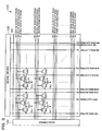
- FIG. 7 shows an outline of a configuration of a liquid crystal device in the embodiment.
- a liquid crystal device 200 in the embodiment may include a liquid crystal panel (display panel in a broad sense) 220.
- a first feature of the liquid crystal panel 220 differing from the liquid crystal panel 120 of the liquid crystal device 100 in the example is that the first to Mth electrodes SS 1 to SS M are removed.
- a third feature is that the switch elements VSW 11 to VSW NM are removed from the pixels P 11 to P NM .
- the pixels are disposed in the shape of a matrix corresponding to intersecting points of the first to Nth scan electrodes G 1 to G N and the first to Mth signal electrodes S 1 to S M in the same manner as in the liquid crystal panel 120 in the example.
- the pixel corresponding to the intersecting point of the jth scan electrode G j and the kth signal electrode S k is indicated by P jk .
- P 11 , P 12 , P 21 , and P 22 are illustrated in FIG. 7, other pixels have the same configuration.
- the liquid crystal device 200 may include a signal driver 230.
- the liquid crystal device 200 may include a scan driver 240.
- a circuit functionally equivalent to the signal driver 230 may be formed on the substrate on which the liquid crystal panel 220 is formed.
- a circuit functionally equivalent to the scan driver 240 may be formed on the substrate.
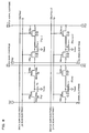
- FIG. 8 is a configuration diagram of the pixels of the liquid crystal device in the embodiment.
- the pixels P jk , P j(k+1) , P (j+1)k , and P (j+1)(k+1) are illustrated.
- the pixel P jk includes the first pixel switch element SW jk and the pixel electrode E jk .
- the gate electrode of the first pixel switch element SW jk is connected with the jth scan electrode G j .
- the source terminal of the first pixel switch element SW jk is connected with the kth signal electrode S k .
- the drain terminal of the first pixel switch element SW jk is connected with the pixel electrode E jk .
- the first pixel switch element SW jk electrically connects the kth signal electrode S k with the pixel electrode E jk based on the voltage of the jth scan electrode G j .
- the pixel P jk may include the second pixel switch element XSW jk .
- the drain terminal of the second pixel switch element XSW jk is connected with the pixel electrode E jk .
- a liquid crystal capacitance is formed by sealing a liquid crystal between the pixel electrode E jk and the common electrode opposite to the pixel electrode E jk .
- the transmittance of the pixel is changed corresponding to the voltage applied between these electrodes.
- the common electrode voltage Vcom is supplied to the common electrode.
- This allows the pixel electrode E jk to be electrically connected with the kth and (M+k)th signal electrodes S k and XS k ( S M+k ).
- the intermediate voltage between the voltage Vp and the voltage Vm is the common electrode voltage Vcom (first voltage in a broad sense).
- FIG. 9A shows a timing chart of the select signal supplied to each scan electrode in the case of changing the voltage applied to the liquid crystal of the pixel from negative to positive.
- the select signal having a pulse width of (tg4 + tg5) is supplied to the jth scan electrode G j . This allows the first and second pixel switch elements SW jk and XSW jk to be turned ON, whereby the voltage of the pixel electrode E jk is set at the common electrode voltage Vcom as described above.
- the pulse width tg4 be smaller than the pulse width tg5, taking drive capability for each electrode into consideration.
- FIG. 9B shows a timing chart of the select signal supplied to each scan electrode in the case of changing the voltage applied to the liquid crystal of the pixel from positive to negative.
- the select signal having a pulse width of tg4 is supplied to the jth scan electrode G j .
- the pulse width tg4 be smaller than the pulse width tg6, taking drive capability for each electrode into consideration.
- FIG. 10 schematically shows a change in voltage of the pixel electrode E jk in the case of changing the voltage applied to the liquid crystal of the pixel from positive to negative.
- the pixel electrodes can be uniformly set at the common electrode voltage Vcom by only transferring charges in the liquid crystal panel 220 without allowing current from the outside to flow. Specifically, since it suffices that charges corresponding to slanted lines 260 be discharged, it is unnecessary to discharge the charges from the voltage Vp to the voltage Vm. This also applies to the case of changing the voltage from negative to positive. As described above, since it suffices that charges be charged or discharged from the common electrode voltage Vcom to either the voltage Vp or the voltage Vm, power consumption accompanied by AC drive can be decreased.
- the configuration of the signal driver 230 can be simplified.
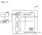
- FIG. 11 shows an example of a functional block diagram of electronic equipment formed by using the liquid crystal device in the above embodiment.
- Electronic equipment 800 includes a liquid crystal device 810, a CPU 820, and a power supply circuit 830.
- the CPU 820 generates image data according to a program stored in a RAM (not shown), and supplies the image data to the liquid crystal device 810.
- the power supply circuit 830 supplies given voltages to the liquid crystal device 810 and the CPU 820.
- the liquid crystal device 810 includes a liquid crystal panel 812, a signal driver 814, a scan driver 816, and a controller 818.
- a liquid crystal panel 812 that of the liquid crystal device 200 in the embodiment may be employed.
- the signal driver 814 drives the signal electrodes of the liquid crystal panel 812.
- the scan driver 816 drives the scan electrodes of the liquid crystal panel 812.
- the controller 818 controls the liquid crystal panel 812 by controlling the signal driver 814 and the scan driver 816 using the image data supplied from the CPU 820 according to timing instructed by the CPU 820.
- liquid crystal projector personal computer, pager, portable telephone, television, view finder or direct view finder video tape recorder, electronic notebook, electronic desk calculator, car navigation system, device provided with a POS terminal or a touch panel, and the like can be given.
- the above embodiments are effective for a display device in which it is difficult to set the voltage required within the select period because one horizontal scanning period (1H) (select period in a broad sense) is short or the load of an interconnect capacitance and the like is great.
- the above embodiments are effective in the case where the size of the display panel is large.
- the present invention is not limited to the above embodiments. Various modifications and variations are possible within the spirit and scope of the present invention. For example, the present invention can be applied to other display devices which perform AC drive.
- the above embodiments are described taking the dot inversion drive method as an example of the AC drive method.
- the present invention can also be applied to the frame inversion drive method or the line inversion drive method.
- the present invention is not limited to the type of the inversion drive method.
Landscapes
- Engineering & Computer Science (AREA)
- Theoretical Computer Science (AREA)
- Physics & Mathematics (AREA)
- Crystallography & Structural Chemistry (AREA)
- Computer Hardware Design (AREA)
- General Physics & Mathematics (AREA)
- Chemical & Material Sciences (AREA)
- Liquid Crystal Display Device Control (AREA)
- Control Of Indicators Other Than Cathode Ray Tubes (AREA)
- Liquid Crystal (AREA)
- Controls And Circuits For Display Device (AREA)
- Devices For Indicating Variable Information By Combining Individual Elements (AREA)
- Transforming Electric Information Into Light Information (AREA)
Applications Claiming Priority (3)
| Application Number | Priority Date | Filing Date | Title |
|---|---|---|---|
| JP2002032676 | 2002-02-08 | ||
| JP2002032676A JP3613246B2 (ja) | 2002-02-08 | 2002-02-08 | 表示装置、その駆動方法及び電子機器 |
| EP03002551A EP1335345B1 (de) | 2002-02-08 | 2003-02-06 | Bildanzeigevorrichtung, Steuerverfahren dafür und elektronisches Gerät |
Related Parent Applications (2)
| Application Number | Title | Priority Date | Filing Date |
|---|---|---|---|
| EP03002551A Division EP1335345B1 (de) | 2002-02-08 | 2003-02-06 | Bildanzeigevorrichtung, Steuerverfahren dafür und elektronisches Gerät |
| EP03002551.4 Division | 2003-02-06 |
Publications (2)
| Publication Number | Publication Date |
|---|---|
| EP1465148A1 true EP1465148A1 (de) | 2004-10-06 |
| EP1465148B1 EP1465148B1 (de) | 2005-09-14 |
Family
ID=27606542
Family Applications (3)
| Application Number | Title | Priority Date | Filing Date |
|---|---|---|---|
| EP04016265A Expired - Lifetime EP1465148B1 (de) | 2002-02-08 | 2003-02-06 | Bildanzeigevorrichtung, Steuerverfahren dafür und elektronisches Gerät |
| EP04016264A Expired - Lifetime EP1467345B1 (de) | 2002-02-08 | 2003-02-06 | Bildanzeigevorrichtung und elektronisches Gerät |
| EP03002551A Expired - Lifetime EP1335345B1 (de) | 2002-02-08 | 2003-02-06 | Bildanzeigevorrichtung, Steuerverfahren dafür und elektronisches Gerät |
Family Applications After (2)
| Application Number | Title | Priority Date | Filing Date |
|---|---|---|---|
| EP04016264A Expired - Lifetime EP1467345B1 (de) | 2002-02-08 | 2003-02-06 | Bildanzeigevorrichtung und elektronisches Gerät |
| EP03002551A Expired - Lifetime EP1335345B1 (de) | 2002-02-08 | 2003-02-06 | Bildanzeigevorrichtung, Steuerverfahren dafür und elektronisches Gerät |
Country Status (8)
| Country | Link |
|---|---|
| US (1) | US7091965B2 (de) |
| EP (3) | EP1465148B1 (de) |
| JP (1) | JP3613246B2 (de) |
| KR (1) | KR100596168B1 (de) |
| CN (1) | CN1262984C (de) |
| AT (3) | ATE345560T1 (de) |
| DE (3) | DE60300547T2 (de) |
| TW (1) | TW589607B (de) |
Families Citing this family (5)
| Publication number | Priority date | Publication date | Assignee | Title |
|---|---|---|---|---|
| TWI253046B (en) * | 2004-05-12 | 2006-04-11 | Au Optronics Corp | Liquid crystal display with improved motion image quality and driving method therefor |
| KR101209051B1 (ko) | 2005-05-04 | 2012-12-06 | 삼성디스플레이 주식회사 | 박막 트랜지스터 표시판 및 그를 포함하는 액정 표시 장치 |
| JP2007121767A (ja) * | 2005-10-28 | 2007-05-17 | Nec Lcd Technologies Ltd | 液晶表示装置 |
| CN102915690A (zh) * | 2011-08-04 | 2013-02-06 | 联咏科技股份有限公司 | 电荷回收装置与相关的面板驱动装置及驱动方法 |
| US9927891B2 (en) | 2012-03-29 | 2018-03-27 | Synaptics Incorporated | System and method for reducing transmitter power consumption |
Citations (2)
| Publication number | Priority date | Publication date | Assignee | Title |
|---|---|---|---|---|
| EP0915453A1 (de) * | 1997-11-07 | 1999-05-12 | Canon Kabushiki Kaisha | Flüssigkristall-Anzeigevorrichtung mit Polaritätsumkehrung |
| EP1158482A2 (de) * | 2000-05-26 | 2001-11-28 | Seiko Epson Corporation | Verfahren zur Ansteuerung eines elektrooptischen Gerätes, Ansteuerschaltung für ein elektrooptisches Gerät, elektrooptisches Gerät und elektronisches Gerät |
Family Cites Families (17)
| Publication number | Priority date | Publication date | Assignee | Title |
|---|---|---|---|---|
| JPS4977537A (de) | 1972-11-27 | 1974-07-26 | ||
| JP2916606B2 (ja) | 1990-11-26 | 1999-07-05 | 株式会社半導体エネルギー研究所 | 表示装置 |
| JP3000174B2 (ja) | 1990-12-10 | 2000-01-17 | 株式会社半導体エネルギー研究所 | 表示装置の駆動方法 |
| FR2674663A1 (fr) | 1991-03-29 | 1992-10-02 | Thomson Lcd | Ecran matriciel a definition amelioree et procede d'adressage d'un tel ecran. |
| KR960002145B1 (ko) * | 1991-07-30 | 1996-02-13 | 가부시기가이샤 히다찌세이사구쇼 | 박막트랜지스터 액정기판의 검사방법 및 그 장치 |
| JPH05273522A (ja) | 1992-01-08 | 1993-10-22 | Matsushita Electric Ind Co Ltd | 表示デバイスおよびそれを用いた表示装置 |
| JP3128965B2 (ja) | 1992-06-25 | 2001-01-29 | ソニー株式会社 | アクティブマトリクス液晶表示装置 |
| JPH0921997A (ja) | 1995-07-07 | 1997-01-21 | Seiko Epson Corp | 液晶表示装置 |
| JPH09114421A (ja) | 1995-10-19 | 1997-05-02 | Asahi Glass Co Ltd | カラー液晶表示装置 |
| US5959599A (en) | 1995-11-07 | 1999-09-28 | Semiconductor Energy Laboratory Co., Ltd. | Active matrix type liquid-crystal display unit and method of driving the same |
| JP3406772B2 (ja) | 1996-03-28 | 2003-05-12 | 株式会社東芝 | アクティブマトリクス型液晶表示装置 |
| US6011530A (en) * | 1996-04-12 | 2000-01-04 | Frontec Incorporated | Liquid crystal display |
| JPH1130975A (ja) * | 1997-05-13 | 1999-02-02 | Oki Electric Ind Co Ltd | 液晶表示装置の駆動回路及びその駆動方法 |
| JPH11101967A (ja) | 1997-07-31 | 1999-04-13 | Toshiba Corp | 液晶表示装置 |
| JP2002023709A (ja) | 2000-07-11 | 2002-01-25 | Seiko Epson Corp | 電気光学装置、およびその駆動方法並びにそれを用いた電子機器 |
| US7170479B2 (en) * | 2002-05-17 | 2007-01-30 | Semiconductor Energy Laboratory Co., Ltd. | Display device and driving method thereof |
| JP2005195810A (ja) * | 2004-01-06 | 2005-07-21 | Nec Electronics Corp | 容量性負荷駆動回路、及び表示パネル駆動回路 |
-
2002
- 2002-02-08 JP JP2002032676A patent/JP3613246B2/ja not_active Expired - Fee Related
-
2003
- 2003-01-10 TW TW092100537A patent/TW589607B/zh not_active IP Right Cessation
- 2003-01-31 CN CNB031042139A patent/CN1262984C/zh not_active Expired - Fee Related
- 2003-02-04 US US10/357,450 patent/US7091965B2/en not_active Expired - Fee Related
- 2003-02-06 EP EP04016265A patent/EP1465148B1/de not_active Expired - Lifetime
- 2003-02-06 AT AT04016264T patent/ATE345560T1/de not_active IP Right Cessation
- 2003-02-06 AT AT04016265T patent/ATE304732T1/de not_active IP Right Cessation
- 2003-02-06 EP EP04016264A patent/EP1467345B1/de not_active Expired - Lifetime
- 2003-02-06 DE DE60300547T patent/DE60300547T2/de not_active Expired - Fee Related
- 2003-02-06 DE DE60301615T patent/DE60301615T2/de not_active Expired - Fee Related
- 2003-02-06 DE DE60309664T patent/DE60309664T2/de not_active Expired - Fee Related
- 2003-02-06 EP EP03002551A patent/EP1335345B1/de not_active Expired - Lifetime
- 2003-02-06 AT AT03002551T patent/ATE294438T1/de not_active IP Right Cessation
- 2003-02-07 KR KR1020030007733A patent/KR100596168B1/ko not_active Expired - Fee Related
Patent Citations (2)
| Publication number | Priority date | Publication date | Assignee | Title |
|---|---|---|---|---|
| EP0915453A1 (de) * | 1997-11-07 | 1999-05-12 | Canon Kabushiki Kaisha | Flüssigkristall-Anzeigevorrichtung mit Polaritätsumkehrung |
| EP1158482A2 (de) * | 2000-05-26 | 2001-11-28 | Seiko Epson Corporation | Verfahren zur Ansteuerung eines elektrooptischen Gerätes, Ansteuerschaltung für ein elektrooptisches Gerät, elektrooptisches Gerät und elektronisches Gerät |
Also Published As
| Publication number | Publication date |
|---|---|
| US7091965B2 (en) | 2006-08-15 |
| DE60300547T2 (de) | 2006-02-16 |
| EP1467345A3 (de) | 2005-03-30 |
| CN1437182A (zh) | 2003-08-20 |
| EP1467345A2 (de) | 2004-10-13 |
| CN1262984C (zh) | 2006-07-05 |
| TW200303004A (en) | 2003-08-16 |
| EP1465148B1 (de) | 2005-09-14 |
| EP1467345B1 (de) | 2006-11-15 |
| DE60301615D1 (de) | 2005-10-20 |
| ATE304732T1 (de) | 2005-09-15 |
| ATE294438T1 (de) | 2005-05-15 |
| DE60301615T2 (de) | 2006-06-08 |
| TW589607B (en) | 2004-06-01 |
| DE60309664T2 (de) | 2007-09-13 |
| DE60309664D1 (de) | 2006-12-28 |
| US20030160747A1 (en) | 2003-08-28 |
| KR20030067575A (ko) | 2003-08-14 |
| JP2003233353A (ja) | 2003-08-22 |
| EP1335345A1 (de) | 2003-08-13 |
| ATE345560T1 (de) | 2006-12-15 |
| DE60300547D1 (de) | 2005-06-02 |
| EP1335345B1 (de) | 2005-04-27 |
| KR100596168B1 (ko) | 2006-07-03 |
| JP3613246B2 (ja) | 2005-01-26 |
Similar Documents
| Publication | Publication Date | Title |
|---|---|---|
| US7079103B2 (en) | Scan-driving circuit, display device, electro-optical device, and scan-driving method | |
| US6211851B1 (en) | Method and apparatus for eliminating crosstalk in active matrix liquid crystal displays | |
| US6075505A (en) | Active matrix liquid crystal display | |
| JP3725458B2 (ja) | アクティブマトリクス表示パネル、およびそれを備えた画像表示装置 | |
| US5805128A (en) | Liquid crystal display device | |
| US7148870B2 (en) | Flat-panel display device | |
| JP2004309669A (ja) | アクティブマトリクス型表示装置とその駆動方法 | |
| JP4694134B2 (ja) | 表示装置 | |
| JP2982877B2 (ja) | アクティブマトリックス液晶表示装置 | |
| JP4420620B2 (ja) | 画像表示装置 | |
| JP3063670B2 (ja) | マトリクス表示装置 | |
| KR100671515B1 (ko) | 액정표시장치의 도트반전구동방법 | |
| JP3147104B2 (ja) | アクティブマトリクス型液晶表示装置とその駆動方法 | |
| US7463232B2 (en) | Thin film transistor LCD structure and driving method thereof | |
| EP1465148B1 (de) | Bildanzeigevorrichtung, Steuerverfahren dafür und elektronisches Gerät | |
| JP3052873B2 (ja) | 液晶表示装置 | |
| JP3638737B2 (ja) | アクティブマトリクス型液晶表示装置およびその駆動方法 | |
| JP4630410B2 (ja) | 液晶表示装置 | |
| JP2006072211A (ja) | 液晶表示装置及び液晶表示装置の駆動方法 | |
| JPH06149174A (ja) | 液晶表示装置 | |
| JP2005128101A (ja) | 液晶表示装置 | |
| JP2003108031A (ja) | 表示装置 | |
| KR101298402B1 (ko) | 액정패널 및 그를 포함하는 액정표시장치 | |
| KR100919191B1 (ko) | 액정표시장치 | |
| JP4622398B2 (ja) | 液晶表示装置及び液晶表示装置の駆動方法 |
Legal Events
| Date | Code | Title | Description |
|---|---|---|---|
| PUAI | Public reference made under article 153(3) epc to a published international application that has entered the european phase |
Free format text: ORIGINAL CODE: 0009012 |
|
| AC | Divisional application: reference to earlier application |
Ref document number: 1335345 Country of ref document: EP Kind code of ref document: P |
|
| AK | Designated contracting states |
Kind code of ref document: A1 Designated state(s): AT BE BG CH CY CZ DE DK EE ES FI FR GB GR HU IE IT LI LU MC NL PT SE SI SK TR |
|
| 17P | Request for examination filed |
Effective date: 20041020 |
|
| GRAP | Despatch of communication of intention to grant a patent |
Free format text: ORIGINAL CODE: EPIDOSNIGR1 |
|
| AKX | Designation fees paid |
Designated state(s): AT BE BG CH CY CZ DE DK EE ES FI FR GB GR HU IE IT LI LU MC NL PT SE SI SK TR |
|
| GRAS | Grant fee paid |
Free format text: ORIGINAL CODE: EPIDOSNIGR3 |
|
| GRAA | (expected) grant |
Free format text: ORIGINAL CODE: 0009210 |
|
| AC | Divisional application: reference to earlier application |
Ref document number: 1335345 Country of ref document: EP Kind code of ref document: P |
|
| AK | Designated contracting states |
Kind code of ref document: B1 Designated state(s): AT BE BG CH CY CZ DE DK EE ES FI FR GB GR HU IE IT LI LU MC NL PT SE SI SK TR |
|
| PG25 | Lapsed in a contracting state [announced via postgrant information from national office to epo] |
Ref country code: IT Free format text: LAPSE BECAUSE OF FAILURE TO SUBMIT A TRANSLATION OF THE DESCRIPTION OR TO PAY THE FEE WITHIN THE PRESCRIBED TIME-LIMIT;WARNING: LAPSES OF ITALIAN PATENTS WITH EFFECTIVE DATE BEFORE 2007 MAY HAVE OCCURRED AT ANY TIME BEFORE 2007. THE CORRECT EFFECTIVE DATE MAY BE DIFFERENT FROM THE ONE RECORDED. Effective date: 20050914 Ref country code: LI Free format text: LAPSE BECAUSE OF FAILURE TO SUBMIT A TRANSLATION OF THE DESCRIPTION OR TO PAY THE FEE WITHIN THE PRESCRIBED TIME-LIMIT Effective date: 20050914 Ref country code: SI Free format text: LAPSE BECAUSE OF FAILURE TO SUBMIT A TRANSLATION OF THE DESCRIPTION OR TO PAY THE FEE WITHIN THE PRESCRIBED TIME-LIMIT Effective date: 20050914 Ref country code: SK Free format text: LAPSE BECAUSE OF FAILURE TO SUBMIT A TRANSLATION OF THE DESCRIPTION OR TO PAY THE FEE WITHIN THE PRESCRIBED TIME-LIMIT Effective date: 20050914 Ref country code: NL Free format text: LAPSE BECAUSE OF FAILURE TO SUBMIT A TRANSLATION OF THE DESCRIPTION OR TO PAY THE FEE WITHIN THE PRESCRIBED TIME-LIMIT Effective date: 20050914 Ref country code: CH Free format text: LAPSE BECAUSE OF FAILURE TO SUBMIT A TRANSLATION OF THE DESCRIPTION OR TO PAY THE FEE WITHIN THE PRESCRIBED TIME-LIMIT Effective date: 20050914 Ref country code: BE Free format text: LAPSE BECAUSE OF FAILURE TO SUBMIT A TRANSLATION OF THE DESCRIPTION OR TO PAY THE FEE WITHIN THE PRESCRIBED TIME-LIMIT Effective date: 20050914 Ref country code: FI Free format text: LAPSE BECAUSE OF FAILURE TO SUBMIT A TRANSLATION OF THE DESCRIPTION OR TO PAY THE FEE WITHIN THE PRESCRIBED TIME-LIMIT Effective date: 20050914 Ref country code: AT Free format text: LAPSE BECAUSE OF FAILURE TO SUBMIT A TRANSLATION OF THE DESCRIPTION OR TO PAY THE FEE WITHIN THE PRESCRIBED TIME-LIMIT Effective date: 20050914 Ref country code: CZ Free format text: LAPSE BECAUSE OF FAILURE TO SUBMIT A TRANSLATION OF THE DESCRIPTION OR TO PAY THE FEE WITHIN THE PRESCRIBED TIME-LIMIT Effective date: 20050914 |
|
| REG | Reference to a national code |
Ref country code: GB Ref legal event code: FG4D |
|
| REG | Reference to a national code |
Ref country code: CH Ref legal event code: EP |
|
| REG | Reference to a national code |
Ref country code: IE Ref legal event code: FG4D |
|
| REF | Corresponds to: |
Ref document number: 60301615 Country of ref document: DE Date of ref document: 20051020 Kind code of ref document: P |
|
| PG25 | Lapsed in a contracting state [announced via postgrant information from national office to epo] |
Ref country code: BG Free format text: LAPSE BECAUSE OF FAILURE TO SUBMIT A TRANSLATION OF THE DESCRIPTION OR TO PAY THE FEE WITHIN THE PRESCRIBED TIME-LIMIT Effective date: 20051214 Ref country code: GR Free format text: LAPSE BECAUSE OF FAILURE TO SUBMIT A TRANSLATION OF THE DESCRIPTION OR TO PAY THE FEE WITHIN THE PRESCRIBED TIME-LIMIT Effective date: 20051214 Ref country code: SE Free format text: LAPSE BECAUSE OF FAILURE TO SUBMIT A TRANSLATION OF THE DESCRIPTION OR TO PAY THE FEE WITHIN THE PRESCRIBED TIME-LIMIT Effective date: 20051214 Ref country code: DK Free format text: LAPSE BECAUSE OF FAILURE TO SUBMIT A TRANSLATION OF THE DESCRIPTION OR TO PAY THE FEE WITHIN THE PRESCRIBED TIME-LIMIT Effective date: 20051214 |
|
| PG25 | Lapsed in a contracting state [announced via postgrant information from national office to epo] |
Ref country code: ES Free format text: LAPSE BECAUSE OF FAILURE TO SUBMIT A TRANSLATION OF THE DESCRIPTION OR TO PAY THE FEE WITHIN THE PRESCRIBED TIME-LIMIT Effective date: 20051225 |
|
| PG25 | Lapsed in a contracting state [announced via postgrant information from national office to epo] |
Ref country code: IE Free format text: LAPSE BECAUSE OF NON-PAYMENT OF DUE FEES Effective date: 20060206 |
|
| PG25 | Lapsed in a contracting state [announced via postgrant information from national office to epo] |
Ref country code: PT Free format text: LAPSE BECAUSE OF FAILURE TO SUBMIT A TRANSLATION OF THE DESCRIPTION OR TO PAY THE FEE WITHIN THE PRESCRIBED TIME-LIMIT Effective date: 20060214 |
|
| PG25 | Lapsed in a contracting state [announced via postgrant information from national office to epo] |
Ref country code: MC Free format text: LAPSE BECAUSE OF NON-PAYMENT OF DUE FEES Effective date: 20060228 Ref country code: LU Free format text: LAPSE BECAUSE OF NON-PAYMENT OF DUE FEES Effective date: 20060228 |
|
| NLV1 | Nl: lapsed or annulled due to failure to fulfill the requirements of art. 29p and 29m of the patents act | ||
| PG25 | Lapsed in a contracting state [announced via postgrant information from national office to epo] |
Ref country code: HU Free format text: LAPSE BECAUSE OF FAILURE TO SUBMIT A TRANSLATION OF THE DESCRIPTION OR TO PAY THE FEE WITHIN THE PRESCRIBED TIME-LIMIT Effective date: 20060315 |
|
| REG | Reference to a national code |
Ref country code: CH Ref legal event code: PL |
|
| ET | Fr: translation filed | ||
| PLBE | No opposition filed within time limit |
Free format text: ORIGINAL CODE: 0009261 |
|
| STAA | Information on the status of an ep patent application or granted ep patent |
Free format text: STATUS: NO OPPOSITION FILED WITHIN TIME LIMIT |
|
| 26N | No opposition filed |
Effective date: 20060615 |
|
| REG | Reference to a national code |
Ref country code: IE Ref legal event code: MM4A |
|
| PG25 | Lapsed in a contracting state [announced via postgrant information from national office to epo] |
Ref country code: EE Free format text: LAPSE BECAUSE OF FAILURE TO SUBMIT A TRANSLATION OF THE DESCRIPTION OR TO PAY THE FEE WITHIN THE PRESCRIBED TIME-LIMIT Effective date: 20050914 |
|
| PG25 | Lapsed in a contracting state [announced via postgrant information from national office to epo] |
Ref country code: TR Free format text: LAPSE BECAUSE OF FAILURE TO SUBMIT A TRANSLATION OF THE DESCRIPTION OR TO PAY THE FEE WITHIN THE PRESCRIBED TIME-LIMIT Effective date: 20050914 |
|
| PG25 | Lapsed in a contracting state [announced via postgrant information from national office to epo] |
Ref country code: CY Free format text: LAPSE BECAUSE OF FAILURE TO SUBMIT A TRANSLATION OF THE DESCRIPTION OR TO PAY THE FEE WITHIN THE PRESCRIBED TIME-LIMIT Effective date: 20050914 |
|
| PGFP | Annual fee paid to national office [announced via postgrant information from national office to epo] |
Ref country code: DE Payment date: 20090129 Year of fee payment: 7 |
|
| PGFP | Annual fee paid to national office [announced via postgrant information from national office to epo] |
Ref country code: GB Payment date: 20090204 Year of fee payment: 7 |
|
| PGFP | Annual fee paid to national office [announced via postgrant information from national office to epo] |
Ref country code: FR Payment date: 20090213 Year of fee payment: 7 |
|
| GBPC | Gb: european patent ceased through non-payment of renewal fee |
Effective date: 20100206 |
|
| REG | Reference to a national code |
Ref country code: FR Ref legal event code: ST Effective date: 20101029 |
|
| PG25 | Lapsed in a contracting state [announced via postgrant information from national office to epo] |
Ref country code: FR Free format text: LAPSE BECAUSE OF NON-PAYMENT OF DUE FEES Effective date: 20100301 |
|
| PG25 | Lapsed in a contracting state [announced via postgrant information from national office to epo] |
Ref country code: DE Free format text: LAPSE BECAUSE OF NON-PAYMENT OF DUE FEES Effective date: 20100901 |
|
| PG25 | Lapsed in a contracting state [announced via postgrant information from national office to epo] |
Ref country code: GB Free format text: LAPSE BECAUSE OF NON-PAYMENT OF DUE FEES Effective date: 20100206 |