EP1465246A2 - Methode zur Herstellung von elektrisch leitenden Durchführungen - Google Patents
Methode zur Herstellung von elektrisch leitenden Durchführungen Download PDFInfo
- Publication number
- EP1465246A2 EP1465246A2 EP04447086A EP04447086A EP1465246A2 EP 1465246 A2 EP1465246 A2 EP 1465246A2 EP 04447086 A EP04447086 A EP 04447086A EP 04447086 A EP04447086 A EP 04447086A EP 1465246 A2 EP1465246 A2 EP 1465246A2
- Authority
- EP
- European Patent Office
- Prior art keywords
- hole
- substrate
- layer
- dielectric
- dielectric material
- Prior art date
- Legal status (The legal status is an assumption and is not a legal conclusion. Google has not performed a legal analysis and makes no representation as to the accuracy of the status listed.)
- Granted
Links
Images




Classifications
-
- H—ELECTRICITY
- H10—SEMICONDUCTOR DEVICES; ELECTRIC SOLID-STATE DEVICES NOT OTHERWISE PROVIDED FOR
- H10W—GENERIC PACKAGES, INTERCONNECTIONS, CONNECTORS OR OTHER CONSTRUCTIONAL DETAILS OF DEVICES COVERED BY CLASS H10
- H10W20/00—Interconnections in chips, wafers or substrates
- H10W20/01—Manufacture or treatment
- H10W20/021—Manufacture or treatment of interconnections within wafers or substrates
- H10W20/023—Manufacture or treatment of interconnections within wafers or substrates the interconnections being through-semiconductor vias
-
- H—ELECTRICITY
- H10—SEMICONDUCTOR DEVICES; ELECTRIC SOLID-STATE DEVICES NOT OTHERWISE PROVIDED FOR
- H10W—GENERIC PACKAGES, INTERCONNECTIONS, CONNECTORS OR OTHER CONSTRUCTIONAL DETAILS OF DEVICES COVERED BY CLASS H10
- H10W20/00—Interconnections in chips, wafers or substrates
- H10W20/01—Manufacture or treatment
- H10W20/021—Manufacture or treatment of interconnections within wafers or substrates
- H10W20/023—Manufacture or treatment of interconnections within wafers or substrates the interconnections being through-semiconductor vias
- H10W20/0234—Manufacture or treatment of interconnections within wafers or substrates the interconnections being through-semiconductor vias comprising etching via holes that stop on pads or on electrodes
-
- H—ELECTRICITY
- H10—SEMICONDUCTOR DEVICES; ELECTRIC SOLID-STATE DEVICES NOT OTHERWISE PROVIDED FOR
- H10W—GENERIC PACKAGES, INTERCONNECTIONS, CONNECTORS OR OTHER CONSTRUCTIONAL DETAILS OF DEVICES COVERED BY CLASS H10
- H10W20/00—Interconnections in chips, wafers or substrates
- H10W20/01—Manufacture or treatment
- H10W20/021—Manufacture or treatment of interconnections within wafers or substrates
- H10W20/023—Manufacture or treatment of interconnections within wafers or substrates the interconnections being through-semiconductor vias
- H10W20/0242—Manufacture or treatment of interconnections within wafers or substrates the interconnections being through-semiconductor vias comprising etching via holes from the back sides of the chips, wafers or substrates
-
- H—ELECTRICITY
- H10—SEMICONDUCTOR DEVICES; ELECTRIC SOLID-STATE DEVICES NOT OTHERWISE PROVIDED FOR
- H10W—GENERIC PACKAGES, INTERCONNECTIONS, CONNECTORS OR OTHER CONSTRUCTIONAL DETAILS OF DEVICES COVERED BY CLASS H10
- H10W20/00—Interconnections in chips, wafers or substrates
- H10W20/01—Manufacture or treatment
- H10W20/021—Manufacture or treatment of interconnections within wafers or substrates
- H10W20/023—Manufacture or treatment of interconnections within wafers or substrates the interconnections being through-semiconductor vias
- H10W20/0245—Manufacture or treatment of interconnections within wafers or substrates the interconnections being through-semiconductor vias comprising use of blind vias during the manufacture
-
- H—ELECTRICITY
- H10—SEMICONDUCTOR DEVICES; ELECTRIC SOLID-STATE DEVICES NOT OTHERWISE PROVIDED FOR
- H10W—GENERIC PACKAGES, INTERCONNECTIONS, CONNECTORS OR OTHER CONSTRUCTIONAL DETAILS OF DEVICES COVERED BY CLASS H10
- H10W20/00—Interconnections in chips, wafers or substrates
- H10W20/01—Manufacture or treatment
- H10W20/021—Manufacture or treatment of interconnections within wafers or substrates
- H10W20/023—Manufacture or treatment of interconnections within wafers or substrates the interconnections being through-semiconductor vias
- H10W20/0265—Manufacture or treatment of interconnections within wafers or substrates the interconnections being through-semiconductor vias characterised by the sidewall insulation
-
- H—ELECTRICITY
- H10—SEMICONDUCTOR DEVICES; ELECTRIC SOLID-STATE DEVICES NOT OTHERWISE PROVIDED FOR
- H10W—GENERIC PACKAGES, INTERCONNECTIONS, CONNECTORS OR OTHER CONSTRUCTIONAL DETAILS OF DEVICES COVERED BY CLASS H10
- H10W20/00—Interconnections in chips, wafers or substrates
- H10W20/20—Interconnections within wafers or substrates, e.g. through-silicon vias [TSV]
-
- H—ELECTRICITY
- H10—SEMICONDUCTOR DEVICES; ELECTRIC SOLID-STATE DEVICES NOT OTHERWISE PROVIDED FOR
- H10W—GENERIC PACKAGES, INTERCONNECTIONS, CONNECTORS OR OTHER CONSTRUCTIONAL DETAILS OF DEVICES COVERED BY CLASS H10
- H10W20/00—Interconnections in chips, wafers or substrates
- H10W20/20—Interconnections within wafers or substrates, e.g. through-silicon vias [TSV]
- H10W20/211—Through-semiconductor vias, e.g. TSVs
- H10W20/212—Top-view shapes or dispositions, e.g. top-view layouts of the vias
- H10W20/2125—Top-view shapes
- H10W20/2128—Coaxial through-semiconductor vias
-
- H—ELECTRICITY
- H10—SEMICONDUCTOR DEVICES; ELECTRIC SOLID-STATE DEVICES NOT OTHERWISE PROVIDED FOR
- H10W—GENERIC PACKAGES, INTERCONNECTIONS, CONNECTORS OR OTHER CONSTRUCTIONAL DETAILS OF DEVICES COVERED BY CLASS H10
- H10W20/00—Interconnections in chips, wafers or substrates
- H10W20/20—Interconnections within wafers or substrates, e.g. through-silicon vias [TSV]
- H10W20/211—Through-semiconductor vias, e.g. TSVs
- H10W20/216—Through-semiconductor vias, e.g. TSVs characterised by dielectric material at least partially filling the via holes, e.g. covering the through-semiconductor vias in the via holes
-
- H—ELECTRICITY
- H10—SEMICONDUCTOR DEVICES; ELECTRIC SOLID-STATE DEVICES NOT OTHERWISE PROVIDED FOR
- H10W—GENERIC PACKAGES, INTERCONNECTIONS, CONNECTORS OR OTHER CONSTRUCTIONAL DETAILS OF DEVICES COVERED BY CLASS H10
- H10W74/00—Encapsulations, e.g. protective coatings
- H10W74/10—Encapsulations, e.g. protective coatings characterised by their shape or disposition
- H10W74/111—Encapsulations, e.g. protective coatings characterised by their shape or disposition the semiconductor body being completely enclosed
- H10W74/129—Encapsulations, e.g. protective coatings characterised by their shape or disposition the semiconductor body being completely enclosed forming a chip-scale package [CSP]
-
- H—ELECTRICITY
- H10—SEMICONDUCTOR DEVICES; ELECTRIC SOLID-STATE DEVICES NOT OTHERWISE PROVIDED FOR
- H10W—GENERIC PACKAGES, INTERCONNECTIONS, CONNECTORS OR OTHER CONSTRUCTIONAL DETAILS OF DEVICES COVERED BY CLASS H10
- H10W20/00—Interconnections in chips, wafers or substrates
- H10W20/01—Manufacture or treatment
- H10W20/071—Manufacture or treatment of dielectric parts thereof
- H10W20/074—Manufacture or treatment of dielectric parts thereof of dielectric parts comprising thin functional dielectric layers, e.g. dielectric etch-stop, barrier, capping or liner layers
- H10W20/076—Manufacture or treatment of dielectric parts thereof of dielectric parts comprising thin functional dielectric layers, e.g. dielectric etch-stop, barrier, capping or liner layers in via holes or trenches
-
- H—ELECTRICITY
- H10—SEMICONDUCTOR DEVICES; ELECTRIC SOLID-STATE DEVICES NOT OTHERWISE PROVIDED FOR
- H10W—GENERIC PACKAGES, INTERCONNECTIONS, CONNECTORS OR OTHER CONSTRUCTIONAL DETAILS OF DEVICES COVERED BY CLASS H10
- H10W72/00—Interconnections or connectors in packages
- H10W72/071—Connecting or disconnecting
- H10W72/072—Connecting or disconnecting of bump connectors
- H10W72/07251—Connecting or disconnecting of bump connectors characterised by changes in properties of the bump connectors during connecting
-
- H—ELECTRICITY
- H10—SEMICONDUCTOR DEVICES; ELECTRIC SOLID-STATE DEVICES NOT OTHERWISE PROVIDED FOR
- H10W—GENERIC PACKAGES, INTERCONNECTIONS, CONNECTORS OR OTHER CONSTRUCTIONAL DETAILS OF DEVICES COVERED BY CLASS H10
- H10W72/00—Interconnections or connectors in packages
- H10W72/20—Bump connectors, e.g. solder bumps or copper pillars; Dummy bumps; Thermal bumps
-
- H—ELECTRICITY
- H10—SEMICONDUCTOR DEVICES; ELECTRIC SOLID-STATE DEVICES NOT OTHERWISE PROVIDED FOR
- H10W—GENERIC PACKAGES, INTERCONNECTIONS, CONNECTORS OR OTHER CONSTRUCTIONAL DETAILS OF DEVICES COVERED BY CLASS H10
- H10W72/00—Interconnections or connectors in packages
- H10W72/20—Bump connectors, e.g. solder bumps or copper pillars; Dummy bumps; Thermal bumps
- H10W72/241—Dispositions, e.g. layouts
- H10W72/244—Dispositions, e.g. layouts relative to underlying supporting features, e.g. bond pads, RDLs or vias
-
- H—ELECTRICITY
- H10—SEMICONDUCTOR DEVICES; ELECTRIC SOLID-STATE DEVICES NOT OTHERWISE PROVIDED FOR
- H10W—GENERIC PACKAGES, INTERCONNECTIONS, CONNECTORS OR OTHER CONSTRUCTIONAL DETAILS OF DEVICES COVERED BY CLASS H10
- H10W72/00—Interconnections or connectors in packages
- H10W72/20—Bump connectors, e.g. solder bumps or copper pillars; Dummy bumps; Thermal bumps
- H10W72/29—Bond pads specially adapted therefor
-
- H—ELECTRICITY
- H10—SEMICONDUCTOR DEVICES; ELECTRIC SOLID-STATE DEVICES NOT OTHERWISE PROVIDED FOR
- H10W—GENERIC PACKAGES, INTERCONNECTIONS, CONNECTORS OR OTHER CONSTRUCTIONAL DETAILS OF DEVICES COVERED BY CLASS H10
- H10W72/00—Interconnections or connectors in packages
- H10W72/90—Bond pads, in general
- H10W72/941—Dispositions of bond pads
- H10W72/9415—Dispositions of bond pads relative to the surface, e.g. recessed, protruding
Definitions
- the present invention is related to the field of electrical interconnection technologies for microelectronics system elements.
- the present invention is related to methods for producing electrical through hole interconnects.
- the present invention aims to provide a novel method for producing via or through hole interconnects between microelectronic elements, which is relatively easy to perform and can be applied relatively cheaply compared to the state of the art.
- the method should for instance be applicable in thin chip technology as MCM (Multi Chip Module) and system in a package (SIP) technology.
- the invention relates to a method for the fabrication of a device comprising electrical through hole interconnects, comprising the following steps:
- At least two of said dielectric holes within the same substrate hole define interconnects, between which a predetermined electromagnetic field is created when they carry a signal.
- the dielectric holes within the same substrate hole can define an N-fold coaxial cable interconnect.
- N typically 2 or 3
- the method further comprises a step of
- the invention also relates to a method for the fabrication of a device comprising electrical through hole interconnects, comprising the steps of
- the method further comprises the steps of:
- the method further comprises the steps of:
- the method reapplies the further steps (I,J,K) for a finite number of times and the backside of said substrate optionally is thinned up until a level (LA) high enough such that the conducting material on the bottom of said layers of conducting material is removed.
- LA level
- the method reapplies the further steps (L,M,N,O,P,Q) for a finite integer number of times and whereby optionally the backside of said substrate is thinned up until a level (LB) high enough such that the conducting material on the bottom of said layers of conducting material is removed.
- LB level
- the conducting material preferably is copper.
- any of the steps (E), (J) or (P) typically creates an interconnection with an external contact.
- the first, the second and further dielectric materials are chosen from the group [polymer, silicone].
- the polymer is benzocyclobutene.
- Said dielectric materials preferably are deposited by spin coating or spray coating or lamination. More preferably they are the same dielectric material.
- the substrate preferably is a processed substrate and more preferably a semiconductor substrate. Most preferably it is a silicon substrate.
- the substrate hole is circular shaped.
- Said dielectric hole is circular or ring shaped.
- the dielectric hole and said substrate hole preferably are concentric.
- the width of said dielectric hole is between 15 ⁇ m and 40 ⁇ m.
- Patterning of the patternable dielectric material typically is performed by plasma-etching or lithography techniques.
- the present invention also relates to chip to wafer bonding and more specifically to an interconnect scheme for already bonded chips.
- This method for the fabrication of a device comprising electrical through hole interconnects comprises the steps of:
- the substrate preferably is a silicon wafer.
- the substrate hole is circular shaped.
- the internal contact is created by flipping said silicon die with an Aluminium pad on its upper surface, said Aluminium pad being covered with an oxide layer.
- the step of dry etching the silicon die is then performed by etching through the silicon die until the oxide layer is reached.
- the step of dry etching the first layer of first dielectric material is performed by etching said oxide layer.
- the second and the third dielectric material are benzocyclobutene (BCB) and the second layer of said second dielectric material and the third layer of said third dielectric material are deposited by BCB spin coating.
- BCB coating can be silicone layers or parylene CVD coatings.
- BCB and silicone layers can also be spray-coated.
- the invention relates to a method for the production of isolated through hole connects in a substrate comprising the steps of:
- the positive working photo resist is applied by spray-coating or electrophoretic deposition. Possibly the opening of said photo resist is done by UV illumination through a mask.
- the additional step is performed of patterning by dry etching said layer of planarising dielectric material, exposing said Cu-post, before applying the step of depositing and patterning a metal interconnect pattern.
- the invention relates to an alternative method for the production of isolated through hole connects in a substrate, comprising the steps of:
- the photo-patterned dielectric layer is photo benzocyclobutene.
- the additional step is performed of depositing a photo-patterned dielectric layer, with contact openings on said Cu-post, before applying the step of depositing and patterning a metal interconnect pattern.
- the substrate preferably is a silicon wafer.
- the substrate hole typically is circular shaped.
- the step of dry etching said substrate is advantageously performed by Reactive Ion Etching - Inductive Coupled Plasma (RIE-ICP).
- the conducting material is copper.
- the planarising dielectric material and said second dielectric material is preferably benzocyclobutene (BCB).
- said second dielectric material is non-photo benzocyclobutene (BCB).
- the metal interconnect pattern is formed by semi-additive electroplated copper lines.
- the substrate is preferably over-etched.
- the invention in another aspect relates to a device comprising electrical through hole interconnects fabricated by any of the methods as described above.
- the invention further relates to a electrical through hole connect, produced by any of the above-described methods.
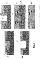
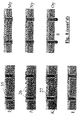
- Fig. 1 illustrates a first embodiment of the present invention.
- Steps 1G and 1H illustrate preferred further optimal steps of the method of the present invention.
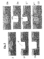
- Fig. 2 represents an embodiment with optimal further steps 2G and 2H of the method of the present invention.
- Fig. 3 represents an embodiment, wherein the method is also applied on the back side of the substrate.
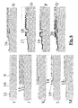
- Fig. 4 represents a sequence of steps according to another embodiment with several layers of dielectric and conducting material.
- Fig. 5 represents an alternative to the embodiment of Fig.4.
- Fig. 6 represents an embodiment related to chip to wafer bonding.
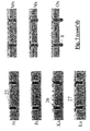
- Fig. 7 represents the steps of an embodiment for a method to create isolated through holes in a substrate.
- Fig. 8 represents an alternative method to that described in Fig. 7.
- the terms 'next layer of dielectric/conducting material' and 'previous layer of dielectric/conducting material' should be understood as the next or previous layer of dielectric/conducting material, respectively, with respect to the moment of deposition.
- the term 'patternable' means that the layer can be patterned. Typically this must be possible at a scale smaller than the hole size.
- the patterning of said patternable dielectric material is performed by plasma-etching and/or lithographic techniques.
- the term 'dielectric hole' is used for a hole whereof the sidewalls are covered with a dielectric material, whereas a 'conductor hole' has sidewalls and bottom covered with a layer of conducting material.
- the various steps of the method are numbered in capitals, starting from A). However, it is not always obligatory to perform all steps in alphabetical order, as some steps can constitute an alternative to certain steps that were previously mentioned. The numbering rather refers to that used in the figures.
- a method is disclosed to make isolated through holes or vias in a substrate.
- through holes are fabricated according to a preferred embodiment as follows :
- the method preferably comprises the following steps (see Fig.1):
- step (C), (D), and (E) are replaced by applying Resin Coated Foils, preferably Resin Coated Copper foils. These foils are positioned on top of the substrate, after which they are pressed against the substrate, and thereby fill the hole(s) with a first layer of resin (preferably BCB) and a copper layer.
- Resin Coated Foils preferably Resin Coated Copper foils.
- an aspect ratio (defined as width / depth
- the optimal steps are :
- the aspect ratios achievable by a single process can be essentially doubled.
- different dielectric holes and thus corresponding interconnects are present in one substrate hole and the dielectric holes are made such that a predetermined electromagnetic field is created between the different interconnects when they carry a signal.
- the interconnect structures are made such that coaxial cable interconnects are produced. Coaxial interconnects that are able to carry signals with frequencies up to 77 GHz and even up to 100 GHz can be achieved when using BCB as dielectric material.
- N-fold interconnects can be provided by creating ring shaped, coaxial dielectric holes or variations thereof. In typical embodiments N equals 2.
- the dielectric holes can be completely filled with conducting material.
- the method comprises -starting from the situation in Fig.4F- the further steps:
- the set of steps (I, J, K) are repeated for a finite integer number of times N, such that N-fold electrical interconnects are produced.
- An additional step of thinning the substrate from the back side until at least a level LA is reached is preferred. This way the invention allows making N-fold 'coaxial cable' interconnects.
- the method comprises -starting from the situation in Fig.5F- the further steps:
- the set of steps (L, M, N, O, P, Q) according to the previous embodiment can also be repeated for a finite integer number of times ( n ), such that n -fold electrical interconnects can be produced.
- An additional step of thinning the substrate from the back side up until a level LB is reached is preferred.
- Step (P) can advantageously create an interconnection with an external contact. This way the invention allows again making n-fold 'coaxial cable' interconnects.
- the present invention offers different advantages. It allows the production of multiple metal connections through a single Si hole. For example it allows for radio frequency (RF) coax transitions.
- RF radio frequency
- the invention also relates to a method for making isolated through holes or vias in a substrate.
- the method comprises according to a preferred embodiment the following steps (Fig.7):
- An alternative method to make isolated through holes or vias in a substrate comprises the following steps (Figure 8). The first three steps are as described above.
- Polymer layers have a low k value and can have a relatively large thickness compared to inorganic layers.
- Polymers like BCB can be deposited at relatively low temperatures, when compared to for instance CVD Si oxide deposition.
- a typical prior art CVD Silicon oxide deposition step in order to create isolated through holes, is limited moreover by the characteristic of bad step coverage properties. Silicon oxide deposition produces layers with about uniform thickness, which limits design freedom. Silicon oxide can easily build up stress and is not flexible.
Landscapes
- Internal Circuitry In Semiconductor Integrated Circuit Devices (AREA)
- Printing Elements For Providing Electric Connections Between Printed Circuits (AREA)
Priority Applications (2)
| Application Number | Priority Date | Filing Date | Title |
|---|---|---|---|
| EP13194159.3A EP2704187B1 (de) | 2003-04-03 | 2004-04-02 | Verfahren zur Herstellung von elektrischen Durchkontaktierungen und damit hergestellte Vorrichtung |
| EP04447086.2A EP1465246B1 (de) | 2003-04-03 | 2004-04-02 | Methode zur Herstellung von elektrisch leitenden Durchführungen |
Applications Claiming Priority (9)
| Application Number | Priority Date | Filing Date | Title |
|---|---|---|---|
| US46085303P | 2003-04-03 | 2003-04-03 | |
| EP03447079 | 2003-04-03 | ||
| EP03447079 | 2003-04-03 | ||
| US460853P | 2003-04-03 | ||
| EP03447236 | 2003-09-22 | ||
| EP03447236A EP1519410A1 (de) | 2003-09-25 | 2003-09-25 | Methode zur Herstellung von elektrisch leitenden Durchführungen |
| US50656003P | 2003-09-26 | 2003-09-26 | |
| US506560P | 2003-09-26 | ||
| EP04447086.2A EP1465246B1 (de) | 2003-04-03 | 2004-04-02 | Methode zur Herstellung von elektrisch leitenden Durchführungen |
Related Child Applications (1)
| Application Number | Title | Priority Date | Filing Date |
|---|---|---|---|
| EP13194159.3A Division EP2704187B1 (de) | 2003-04-03 | 2004-04-02 | Verfahren zur Herstellung von elektrischen Durchkontaktierungen und damit hergestellte Vorrichtung |
Publications (3)
| Publication Number | Publication Date |
|---|---|
| EP1465246A2 true EP1465246A2 (de) | 2004-10-06 |
| EP1465246A3 EP1465246A3 (de) | 2005-03-16 |
| EP1465246B1 EP1465246B1 (de) | 2013-12-18 |
Family
ID=32854523
Family Applications (2)
| Application Number | Title | Priority Date | Filing Date |
|---|---|---|---|
| EP04447086.2A Expired - Lifetime EP1465246B1 (de) | 2003-04-03 | 2004-04-02 | Methode zur Herstellung von elektrisch leitenden Durchführungen |
| EP13194159.3A Expired - Lifetime EP2704187B1 (de) | 2003-04-03 | 2004-04-02 | Verfahren zur Herstellung von elektrischen Durchkontaktierungen und damit hergestellte Vorrichtung |
Family Applications After (1)
| Application Number | Title | Priority Date | Filing Date |
|---|---|---|---|
| EP13194159.3A Expired - Lifetime EP2704187B1 (de) | 2003-04-03 | 2004-04-02 | Verfahren zur Herstellung von elektrischen Durchkontaktierungen und damit hergestellte Vorrichtung |
Country Status (1)
| Country | Link |
|---|---|
| EP (2) | EP1465246B1 (de) |
Cited By (6)
| Publication number | Priority date | Publication date | Assignee | Title |
|---|---|---|---|---|
| US8633572B2 (en) | 2006-03-27 | 2014-01-21 | Koninklijke Philips N.V. | Low ohmic through substrate interconnection for semiconductor carriers |
| EP2388814A3 (de) * | 2010-05-21 | 2014-04-23 | Napra Co., Ltd. | Elektronische Vorrichtung und Herstellungsverfahren dafür |
| US8791005B2 (en) | 2012-06-18 | 2014-07-29 | International Business Machines Corporation | Sidewalls of electroplated copper interconnects |
| WO2015134279A1 (en) * | 2014-03-04 | 2015-09-11 | Qualcomm Incorporated | Substrate with conductive vias |
| CN115053331A (zh) * | 2020-03-10 | 2022-09-13 | 国际商业机器公司 | 高带宽模块 |
| CN117504960A (zh) * | 2023-11-23 | 2024-02-06 | 西安稀有金属材料研究院有限公司 | 微流道制备方法 |
Citations (1)
| Publication number | Priority date | Publication date | Assignee | Title |
|---|---|---|---|---|
| US20020027293A1 (en) | 2001-06-28 | 2002-03-07 | Fujitsu Limited | Three dimensional semiconductor integrated circuit device and method for making the same |
Family Cites Families (6)
| Publication number | Priority date | Publication date | Assignee | Title |
|---|---|---|---|---|
| JPS61248534A (ja) * | 1985-04-26 | 1986-11-05 | Toshiba Corp | 絶縁膜の形成方法 |
| EP0948808A4 (de) | 1996-10-29 | 2000-05-10 | Trusi Technologies Llc | Integrierte schaltungen und verfahren zur herstellung |
| US6222276B1 (en) * | 1998-04-07 | 2001-04-24 | International Business Machines Corporation | Through-chip conductors for low inductance chip-to-chip integration and off-chip connections |
| JP4547728B2 (ja) * | 1999-03-29 | 2010-09-22 | ソニー株式会社 | 半導体装置及びその製造方法 |
| JP3951091B2 (ja) * | 2000-08-04 | 2007-08-01 | セイコーエプソン株式会社 | 半導体装置の製造方法 |
| EP1199744B1 (de) * | 2000-10-19 | 2005-12-28 | Agilent Technologies, Inc. (a Delaware corporation) | Mikrodeckelgehäuse auf Scheibenebene |
-
2004
- 2004-04-02 EP EP04447086.2A patent/EP1465246B1/de not_active Expired - Lifetime
- 2004-04-02 EP EP13194159.3A patent/EP2704187B1/de not_active Expired - Lifetime
Patent Citations (1)
| Publication number | Priority date | Publication date | Assignee | Title |
|---|---|---|---|---|
| US20020027293A1 (en) | 2001-06-28 | 2002-03-07 | Fujitsu Limited | Three dimensional semiconductor integrated circuit device and method for making the same |
Cited By (11)
| Publication number | Priority date | Publication date | Assignee | Title |
|---|---|---|---|---|
| US8633572B2 (en) | 2006-03-27 | 2014-01-21 | Koninklijke Philips N.V. | Low ohmic through substrate interconnection for semiconductor carriers |
| EP2388814A3 (de) * | 2010-05-21 | 2014-04-23 | Napra Co., Ltd. | Elektronische Vorrichtung und Herstellungsverfahren dafür |
| US9685394B2 (en) | 2010-05-21 | 2017-06-20 | Napra Co., Ltd. | Electronic device and manufacturing method therefor |
| US8791005B2 (en) | 2012-06-18 | 2014-07-29 | International Business Machines Corporation | Sidewalls of electroplated copper interconnects |
| US9040407B2 (en) | 2012-06-18 | 2015-05-26 | International Business Machines Corporation | Sidewalls of electroplated copper interconnects |
| US9055703B2 (en) | 2012-06-18 | 2015-06-09 | International Business Machines Corporation | Sidewalls of electroplated copper interconnects |
| US9060457B2 (en) | 2012-06-18 | 2015-06-16 | International Business Machines Corporation | Sidewalls of electroplated copper interconnects |
| WO2015134279A1 (en) * | 2014-03-04 | 2015-09-11 | Qualcomm Incorporated | Substrate with conductive vias |
| US9596768B2 (en) | 2014-03-04 | 2017-03-14 | Qualcomm Incorporated | Substrate with conductive vias |
| CN115053331A (zh) * | 2020-03-10 | 2022-09-13 | 国际商业机器公司 | 高带宽模块 |
| CN117504960A (zh) * | 2023-11-23 | 2024-02-06 | 西安稀有金属材料研究院有限公司 | 微流道制备方法 |
Also Published As
| Publication number | Publication date |
|---|---|
| EP1465246B1 (de) | 2013-12-18 |
| EP2704187A1 (de) | 2014-03-05 |
| EP2704187B1 (de) | 2015-08-19 |
| EP1465246A3 (de) | 2005-03-16 |
Similar Documents
| Publication | Publication Date | Title |
|---|---|---|
| US20040259292A1 (en) | Method for producing electrical through hole interconnects and devices made thereof | |
| EP1519410A1 (de) | Methode zur Herstellung von elektrisch leitenden Durchführungen | |
| EP2201600B1 (de) | Verfahren zur herstellung von substratdurchkontaktierungen | |
| US8390125B2 (en) | Through-silicon via formed with a post passivation interconnect structure | |
| US9818698B2 (en) | EMI package and method for making same | |
| US8405191B2 (en) | Semiconductor device structures | |
| US6153521A (en) | Metallized interconnection structure and method of making the same | |
| CN101622700B (zh) | 利用电镀的导电过孔形成 | |
| US5112448A (en) | Self-aligned process for fabrication of interconnect structures in semiconductor applications | |
| JP3630777B2 (ja) | マルチチップ・モジュールの製造方法 | |
| US6878608B2 (en) | Method of manufacture of silicon based package | |
| US8975753B2 (en) | Three dimensional interconnect structure and method thereof | |
| US20200126894A1 (en) | Integrated passive device and fabrication method using a last through-substrate via | |
| EP2826066B1 (de) | Halbleiterbauelemente mit dichtgepackten durchkontaktierungen und ebener umverdrahtung, sowie verfahren zur herstellung davon | |
| US4705606A (en) | Thin-film electrical connections for integrated circuits | |
| JPH04359518A (ja) | 半導体装置の製造方法 | |
| KR20100108293A (ko) | 비아 구조 및 그것을 형성하는 비아에칭 방법 | |
| WO2004109770A2 (en) | Through wafer via process and amplifier with through wafer via | |
| EP2704187B1 (de) | Verfahren zur Herstellung von elektrischen Durchkontaktierungen und damit hergestellte Vorrichtung | |
| US9576882B2 (en) | Through polymer via (TPV) and method to manufacture such a via | |
| US7427565B2 (en) | Multi-step etch for metal bump formation | |
| JP4154478B2 (ja) | 感光性ポリイミドを用いた貫通電極形成方法 | |
| US12191203B2 (en) | Semiconductor package | |
| US20260068616A1 (en) | Package structure and method of manufacturing the same | |
| CN117038575A (zh) | 简易硅基垂直互连封装方法、装置及基板 |
Legal Events
| Date | Code | Title | Description |
|---|---|---|---|
| PUAI | Public reference made under article 153(3) epc to a published international application that has entered the european phase |
Free format text: ORIGINAL CODE: 0009012 |
|
| AK | Designated contracting states |
Kind code of ref document: A2 Designated state(s): AT BE BG CH CY CZ DE DK EE ES FI FR GB GR HU IE IT LI LU MC NL PL PT RO SE SI SK TR |
|
| AX | Request for extension of the european patent |
Extension state: AL HR LT LV MK |
|
| PUAL | Search report despatched |
Free format text: ORIGINAL CODE: 0009013 |
|
| AK | Designated contracting states |
Kind code of ref document: A3 Designated state(s): AT BE BG CH CY CZ DE DK EE ES FI FR GB GR HU IE IT LI LU MC NL PL PT RO SE SI SK TR |
|
| AX | Request for extension of the european patent |
Extension state: AL HR LT LV MK |
|
| 17P | Request for examination filed |
Effective date: 20050504 |
|
| AKX | Designation fees paid |
Designated state(s): AT BE BG CH CY CZ DE DK EE ES FI FR GB GR HU IE IT LI LU MC NL PL PT RO SE SI SK TR |
|
| RAP1 | Party data changed (applicant data changed or rights of an application transferred) |
Owner name: IMEC |
|
| 17Q | First examination report despatched |
Effective date: 20120316 |
|
| GRAP | Despatch of communication of intention to grant a patent |
Free format text: ORIGINAL CODE: EPIDOSNIGR1 |
|
| RIN1 | Information on inventor provided before grant (corrected) |
Inventor name: LABLE, RIET Inventor name: BEYNE, ERIC |
|
| INTG | Intention to grant announced |
Effective date: 20130708 |
|
| RIN1 | Information on inventor provided before grant (corrected) |
Inventor name: LABIE, RIET Inventor name: BEYNE, ERIC |
|
| GRAS | Grant fee paid |
Free format text: ORIGINAL CODE: EPIDOSNIGR3 |
|
| GRAA | (expected) grant |
Free format text: ORIGINAL CODE: 0009210 |
|
| AK | Designated contracting states |
Kind code of ref document: B1 Designated state(s): AT BE BG CH CY CZ DE DK EE ES FI FR GB GR HU IE IT LI LU MC NL PL PT RO SE SI SK TR |
|
| REG | Reference to a national code |
Ref country code: GB Ref legal event code: FG4D |
|
| REG | Reference to a national code |
Ref country code: CH Ref legal event code: EP |
|
| REG | Reference to a national code |
Ref country code: AT Ref legal event code: REF Ref document number: 645941 Country of ref document: AT Kind code of ref document: T Effective date: 20140115 |
|
| REG | Reference to a national code |
Ref country code: IE Ref legal event code: FG4D |
|
| REG | Reference to a national code |
Ref country code: DE Ref legal event code: R096 Ref document number: 602004044010 Country of ref document: DE Effective date: 20140213 |
|
| REG | Reference to a national code |
Ref country code: NL Ref legal event code: VDEP Effective date: 20131218 |
|
| PG25 | Lapsed in a contracting state [announced via postgrant information from national office to epo] |
Ref country code: SE Free format text: LAPSE BECAUSE OF FAILURE TO SUBMIT A TRANSLATION OF THE DESCRIPTION OR TO PAY THE FEE WITHIN THE PRESCRIBED TIME-LIMIT Effective date: 20131218 Ref country code: FI Free format text: LAPSE BECAUSE OF FAILURE TO SUBMIT A TRANSLATION OF THE DESCRIPTION OR TO PAY THE FEE WITHIN THE PRESCRIBED TIME-LIMIT Effective date: 20131218 |
|
| REG | Reference to a national code |
Ref country code: AT Ref legal event code: MK05 Ref document number: 645941 Country of ref document: AT Kind code of ref document: T Effective date: 20131218 |
|
| PG25 | Lapsed in a contracting state [announced via postgrant information from national office to epo] |
Ref country code: BE Free format text: LAPSE BECAUSE OF FAILURE TO SUBMIT A TRANSLATION OF THE DESCRIPTION OR TO PAY THE FEE WITHIN THE PRESCRIBED TIME-LIMIT Effective date: 20131218 Ref country code: EE Free format text: LAPSE BECAUSE OF FAILURE TO SUBMIT A TRANSLATION OF THE DESCRIPTION OR TO PAY THE FEE WITHIN THE PRESCRIBED TIME-LIMIT Effective date: 20131218 |
|
| PG25 | Lapsed in a contracting state [announced via postgrant information from national office to epo] |
Ref country code: CY Free format text: LAPSE BECAUSE OF FAILURE TO SUBMIT A TRANSLATION OF THE DESCRIPTION OR TO PAY THE FEE WITHIN THE PRESCRIBED TIME-LIMIT Effective date: 20131218 Ref country code: AT Free format text: LAPSE BECAUSE OF FAILURE TO SUBMIT A TRANSLATION OF THE DESCRIPTION OR TO PAY THE FEE WITHIN THE PRESCRIBED TIME-LIMIT Effective date: 20131218 Ref country code: RO Free format text: LAPSE BECAUSE OF FAILURE TO SUBMIT A TRANSLATION OF THE DESCRIPTION OR TO PAY THE FEE WITHIN THE PRESCRIBED TIME-LIMIT Effective date: 20131218 Ref country code: SK Free format text: LAPSE BECAUSE OF FAILURE TO SUBMIT A TRANSLATION OF THE DESCRIPTION OR TO PAY THE FEE WITHIN THE PRESCRIBED TIME-LIMIT Effective date: 20131218 Ref country code: NL Free format text: LAPSE BECAUSE OF FAILURE TO SUBMIT A TRANSLATION OF THE DESCRIPTION OR TO PAY THE FEE WITHIN THE PRESCRIBED TIME-LIMIT Effective date: 20131218 Ref country code: ES Free format text: LAPSE BECAUSE OF FAILURE TO SUBMIT A TRANSLATION OF THE DESCRIPTION OR TO PAY THE FEE WITHIN THE PRESCRIBED TIME-LIMIT Effective date: 20131218 Ref country code: CZ Free format text: LAPSE BECAUSE OF FAILURE TO SUBMIT A TRANSLATION OF THE DESCRIPTION OR TO PAY THE FEE WITHIN THE PRESCRIBED TIME-LIMIT Effective date: 20131218 Ref country code: PL Free format text: LAPSE BECAUSE OF FAILURE TO SUBMIT A TRANSLATION OF THE DESCRIPTION OR TO PAY THE FEE WITHIN THE PRESCRIBED TIME-LIMIT Effective date: 20131218 Ref country code: PT Free format text: LAPSE BECAUSE OF FAILURE TO SUBMIT A TRANSLATION OF THE DESCRIPTION OR TO PAY THE FEE WITHIN THE PRESCRIBED TIME-LIMIT Effective date: 20140418 |
|
| REG | Reference to a national code |
Ref country code: DE Ref legal event code: R097 Ref document number: 602004044010 Country of ref document: DE |
|
| PLBE | No opposition filed within time limit |
Free format text: ORIGINAL CODE: 0009261 |
|
| STAA | Information on the status of an ep patent application or granted ep patent |
Free format text: STATUS: NO OPPOSITION FILED WITHIN TIME LIMIT |
|
| PG25 | Lapsed in a contracting state [announced via postgrant information from national office to epo] |
Ref country code: DK Free format text: LAPSE BECAUSE OF FAILURE TO SUBMIT A TRANSLATION OF THE DESCRIPTION OR TO PAY THE FEE WITHIN THE PRESCRIBED TIME-LIMIT Effective date: 20131218 |
|
| 26N | No opposition filed |
Effective date: 20140919 |
|
| PG25 | Lapsed in a contracting state [announced via postgrant information from national office to epo] |
Ref country code: LU Free format text: LAPSE BECAUSE OF FAILURE TO SUBMIT A TRANSLATION OF THE DESCRIPTION OR TO PAY THE FEE WITHIN THE PRESCRIBED TIME-LIMIT Effective date: 20140402 Ref country code: MC Free format text: LAPSE BECAUSE OF FAILURE TO SUBMIT A TRANSLATION OF THE DESCRIPTION OR TO PAY THE FEE WITHIN THE PRESCRIBED TIME-LIMIT Effective date: 20131218 |
|
| REG | Reference to a national code |
Ref country code: CH Ref legal event code: PL |
|
| REG | Reference to a national code |
Ref country code: DE Ref legal event code: R097 Ref document number: 602004044010 Country of ref document: DE Effective date: 20140919 |
|
| REG | Reference to a national code |
Ref country code: IE Ref legal event code: MM4A |
|
| PG25 | Lapsed in a contracting state [announced via postgrant information from national office to epo] |
Ref country code: LI Free format text: LAPSE BECAUSE OF NON-PAYMENT OF DUE FEES Effective date: 20140430 Ref country code: CH Free format text: LAPSE BECAUSE OF NON-PAYMENT OF DUE FEES Effective date: 20140430 |
|
| PG25 | Lapsed in a contracting state [announced via postgrant information from national office to epo] |
Ref country code: IE Free format text: LAPSE BECAUSE OF NON-PAYMENT OF DUE FEES Effective date: 20140402 |
|
| PG25 | Lapsed in a contracting state [announced via postgrant information from national office to epo] |
Ref country code: SI Free format text: LAPSE BECAUSE OF FAILURE TO SUBMIT A TRANSLATION OF THE DESCRIPTION OR TO PAY THE FEE WITHIN THE PRESCRIBED TIME-LIMIT Effective date: 20131218 |
|
| REG | Reference to a national code |
Ref country code: FR Ref legal event code: PLFP Year of fee payment: 13 |
|
| PG25 | Lapsed in a contracting state [announced via postgrant information from national office to epo] |
Ref country code: BG Free format text: LAPSE BECAUSE OF FAILURE TO SUBMIT A TRANSLATION OF THE DESCRIPTION OR TO PAY THE FEE WITHIN THE PRESCRIBED TIME-LIMIT Effective date: 20131218 |
|
| PG25 | Lapsed in a contracting state [announced via postgrant information from national office to epo] |
Ref country code: IT Free format text: LAPSE BECAUSE OF FAILURE TO SUBMIT A TRANSLATION OF THE DESCRIPTION OR TO PAY THE FEE WITHIN THE PRESCRIBED TIME-LIMIT Effective date: 20131218 Ref country code: GR Free format text: LAPSE BECAUSE OF FAILURE TO SUBMIT A TRANSLATION OF THE DESCRIPTION OR TO PAY THE FEE WITHIN THE PRESCRIBED TIME-LIMIT Effective date: 20140319 |
|
| PG25 | Lapsed in a contracting state [announced via postgrant information from national office to epo] |
Ref country code: HU Free format text: LAPSE BECAUSE OF FAILURE TO SUBMIT A TRANSLATION OF THE DESCRIPTION OR TO PAY THE FEE WITHIN THE PRESCRIBED TIME-LIMIT; INVALID AB INITIO Effective date: 20040402 Ref country code: TR Free format text: LAPSE BECAUSE OF FAILURE TO SUBMIT A TRANSLATION OF THE DESCRIPTION OR TO PAY THE FEE WITHIN THE PRESCRIBED TIME-LIMIT Effective date: 20131218 |
|
| REG | Reference to a national code |
Ref country code: FR Ref legal event code: PLFP Year of fee payment: 14 |
|
| REG | Reference to a national code |
Ref country code: FR Ref legal event code: PLFP Year of fee payment: 15 |
|
| PGFP | Annual fee paid to national office [announced via postgrant information from national office to epo] |
Ref country code: GB Payment date: 20200323 Year of fee payment: 17 |
|
| PGFP | Annual fee paid to national office [announced via postgrant information from national office to epo] |
Ref country code: FR Payment date: 20200319 Year of fee payment: 17 |
|
| PGFP | Annual fee paid to national office [announced via postgrant information from national office to epo] |
Ref country code: DE Payment date: 20200319 Year of fee payment: 17 |
|
| REG | Reference to a national code |
Ref country code: DE Ref legal event code: R119 Ref document number: 602004044010 Country of ref document: DE |
|
| GBPC | Gb: european patent ceased through non-payment of renewal fee |
Effective date: 20210402 |
|
| PG25 | Lapsed in a contracting state [announced via postgrant information from national office to epo] |
Ref country code: FR Free format text: LAPSE BECAUSE OF NON-PAYMENT OF DUE FEES Effective date: 20210430 Ref country code: GB Free format text: LAPSE BECAUSE OF NON-PAYMENT OF DUE FEES Effective date: 20210402 Ref country code: DE Free format text: LAPSE BECAUSE OF NON-PAYMENT OF DUE FEES Effective date: 20211103 |