EP1465249A2 - Système et méthode d'aération d'un circuit intégré scellé par un capôt - Google Patents
Système et méthode d'aération d'un circuit intégré scellé par un capôt Download PDFInfo
- Publication number
- EP1465249A2 EP1465249A2 EP04251989A EP04251989A EP1465249A2 EP 1465249 A2 EP1465249 A2 EP 1465249A2 EP 04251989 A EP04251989 A EP 04251989A EP 04251989 A EP04251989 A EP 04251989A EP 1465249 A2 EP1465249 A2 EP 1465249A2
- Authority
- EP
- European Patent Office
- Prior art keywords
- integrated circuit
- substrate
- lid
- opening
- solder
- Prior art date
- Legal status (The legal status is an assumption and is not a legal conclusion. Google has not performed a legal analysis and makes no representation as to the accuracy of the status listed.)
- Granted
Links
Images


Classifications
-
- H—ELECTRICITY
- H10—SEMICONDUCTOR DEVICES; ELECTRIC SOLID-STATE DEVICES NOT OTHERWISE PROVIDED FOR
- H10W—GENERIC PACKAGES, INTERCONNECTIONS, CONNECTORS OR OTHER CONSTRUCTIONAL DETAILS OF DEVICES COVERED BY CLASS H10
- H10W42/00—Arrangements for protection of devices
- H10W42/121—Arrangements for protection of devices protecting against mechanical damage
-
- H—ELECTRICITY
- H05—ELECTRIC TECHNIQUES NOT OTHERWISE PROVIDED FOR
- H05K—PRINTED CIRCUITS; CASINGS OR CONSTRUCTIONAL DETAILS OF ELECTRIC APPARATUS; MANUFACTURE OF ASSEMBLAGES OF ELECTRICAL COMPONENTS
- H05K3/00—Apparatus or processes for manufacturing printed circuits
- H05K3/30—Assembling printed circuits with electric components, e.g. with resistors
- H05K3/32—Assembling printed circuits with electric components, e.g. with resistors electrically connecting electric components or wires to printed circuits
- H05K3/34—Assembling printed circuits with electric components, e.g. with resistors electrically connecting electric components or wires to printed circuits by soldering
- H05K3/341—Surface mounted components
-
- H—ELECTRICITY
- H10—SEMICONDUCTOR DEVICES; ELECTRIC SOLID-STATE DEVICES NOT OTHERWISE PROVIDED FOR
- H10W—GENERIC PACKAGES, INTERCONNECTIONS, CONNECTORS OR OTHER CONSTRUCTIONAL DETAILS OF DEVICES COVERED BY CLASS H10
- H10W40/00—Arrangements for thermal protection or thermal control
- H10W40/10—Arrangements for heating
-
- H—ELECTRICITY
- H10—SEMICONDUCTOR DEVICES; ELECTRIC SOLID-STATE DEVICES NOT OTHERWISE PROVIDED FOR
- H10W—GENERIC PACKAGES, INTERCONNECTIONS, CONNECTORS OR OTHER CONSTRUCTIONAL DETAILS OF DEVICES COVERED BY CLASS H10
- H10W40/00—Arrangements for thermal protection or thermal control
- H10W40/20—Arrangements for cooling
- H10W40/22—Arrangements for cooling characterised by their shape, e.g. having conical or cylindrical projections
- H10W40/226—Arrangements for cooling characterised by their shape, e.g. having conical or cylindrical projections characterised by projecting parts, e.g. fins to increase surface area
- H10W40/228—Arrangements for cooling characterised by their shape, e.g. having conical or cylindrical projections characterised by projecting parts, e.g. fins to increase surface area the projecting parts being wire-shaped or pin-shaped
-
- H—ELECTRICITY
- H10—SEMICONDUCTOR DEVICES; ELECTRIC SOLID-STATE DEVICES NOT OTHERWISE PROVIDED FOR
- H10W—GENERIC PACKAGES, INTERCONNECTIONS, CONNECTORS OR OTHER CONSTRUCTIONAL DETAILS OF DEVICES COVERED BY CLASS H10
- H10W70/00—Package substrates; Interposers; Redistribution layers [RDL]
- H10W70/60—Insulating or insulated package substrates; Interposers; Redistribution layers
- H10W70/67—Insulating or insulated package substrates; Interposers; Redistribution layers characterised by their insulating layers or insulating parts
- H10W70/68—Shapes or dispositions thereof
-
- H—ELECTRICITY
- H10—SEMICONDUCTOR DEVICES; ELECTRIC SOLID-STATE DEVICES NOT OTHERWISE PROVIDED FOR
- H10W—GENERIC PACKAGES, INTERCONNECTIONS, CONNECTORS OR OTHER CONSTRUCTIONAL DETAILS OF DEVICES COVERED BY CLASS H10
- H10W74/00—Encapsulations, e.g. protective coatings
- H10W74/10—Encapsulations, e.g. protective coatings characterised by their shape or disposition
- H10W74/111—Encapsulations, e.g. protective coatings characterised by their shape or disposition the semiconductor body being completely enclosed
- H10W74/114—Encapsulations, e.g. protective coatings characterised by their shape or disposition the semiconductor body being completely enclosed by a substrate and the encapsulations
- H10W74/117—Encapsulations, e.g. protective coatings characterised by their shape or disposition the semiconductor body being completely enclosed by a substrate and the encapsulations the substrate having spherical bumps for external connection
-
- H—ELECTRICITY
- H05—ELECTRIC TECHNIQUES NOT OTHERWISE PROVIDED FOR
- H05K—PRINTED CIRCUITS; CASINGS OR CONSTRUCTIONAL DETAILS OF ELECTRIC APPARATUS; MANUFACTURE OF ASSEMBLAGES OF ELECTRICAL COMPONENTS
- H05K2203/00—Indexing scheme relating to apparatus or processes for manufacturing printed circuits covered by H05K3/00
- H05K2203/11—Treatments characterised by their effect, e.g. heating, cooling, roughening
- H05K2203/1178—Means for venting or for letting gases escape
-
- H—ELECTRICITY
- H05—ELECTRIC TECHNIQUES NOT OTHERWISE PROVIDED FOR
- H05K—PRINTED CIRCUITS; CASINGS OR CONSTRUCTIONAL DETAILS OF ELECTRIC APPARATUS; MANUFACTURE OF ASSEMBLAGES OF ELECTRICAL COMPONENTS
- H05K2203/00—Indexing scheme relating to apparatus or processes for manufacturing printed circuits covered by H05K3/00
- H05K2203/30—Details of processes not otherwise provided for in H05K2203/01 - H05K2203/17
- H05K2203/304—Protecting a component during manufacturing
-
- H—ELECTRICITY
- H10—SEMICONDUCTOR DEVICES; ELECTRIC SOLID-STATE DEVICES NOT OTHERWISE PROVIDED FOR
- H10W—GENERIC PACKAGES, INTERCONNECTIONS, CONNECTORS OR OTHER CONSTRUCTIONAL DETAILS OF DEVICES COVERED BY CLASS H10
- H10W40/00—Arrangements for thermal protection or thermal control
- H10W40/70—Fillings or auxiliary members in containers or in encapsulations for thermal protection or control
- H10W40/77—Auxiliary members characterised by their shape
- H10W40/778—Auxiliary members characterised by their shape in encapsulations
-
- H—ELECTRICITY
- H10—SEMICONDUCTOR DEVICES; ELECTRIC SOLID-STATE DEVICES NOT OTHERWISE PROVIDED FOR
- H10W—GENERIC PACKAGES, INTERCONNECTIONS, CONNECTORS OR OTHER CONSTRUCTIONAL DETAILS OF DEVICES COVERED BY CLASS H10
- H10W70/00—Package substrates; Interposers; Redistribution layers [RDL]
- H10W70/60—Insulating or insulated package substrates; Interposers; Redistribution layers
- H10W70/67—Insulating or insulated package substrates; Interposers; Redistribution layers characterised by their insulating layers or insulating parts
- H10W70/68—Shapes or dispositions thereof
- H10W70/682—Shapes or dispositions thereof comprising holes having chips therein
-
- H—ELECTRICITY
- H10—SEMICONDUCTOR DEVICES; ELECTRIC SOLID-STATE DEVICES NOT OTHERWISE PROVIDED FOR
- H10W—GENERIC PACKAGES, INTERCONNECTIONS, CONNECTORS OR OTHER CONSTRUCTIONAL DETAILS OF DEVICES COVERED BY CLASS H10
- H10W70/00—Package substrates; Interposers; Redistribution layers [RDL]
- H10W70/60—Insulating or insulated package substrates; Interposers; Redistribution layers
- H10W70/67—Insulating or insulated package substrates; Interposers; Redistribution layers characterised by their insulating layers or insulating parts
- H10W70/68—Shapes or dispositions thereof
- H10W70/685—Shapes or dispositions thereof comprising multiple insulating layers
-
- H—ELECTRICITY
- H10—SEMICONDUCTOR DEVICES; ELECTRIC SOLID-STATE DEVICES NOT OTHERWISE PROVIDED FOR
- H10W—GENERIC PACKAGES, INTERCONNECTIONS, CONNECTORS OR OTHER CONSTRUCTIONAL DETAILS OF DEVICES COVERED BY CLASS H10
- H10W72/00—Interconnections or connectors in packages
- H10W72/071—Connecting or disconnecting
- H10W72/075—Connecting or disconnecting of bond wires
-
- H—ELECTRICITY
- H10—SEMICONDUCTOR DEVICES; ELECTRIC SOLID-STATE DEVICES NOT OTHERWISE PROVIDED FOR
- H10W—GENERIC PACKAGES, INTERCONNECTIONS, CONNECTORS OR OTHER CONSTRUCTIONAL DETAILS OF DEVICES COVERED BY CLASS H10
- H10W72/00—Interconnections or connectors in packages
- H10W72/50—Bond wires
- H10W72/551—Materials of bond wires
-
- H—ELECTRICITY
- H10—SEMICONDUCTOR DEVICES; ELECTRIC SOLID-STATE DEVICES NOT OTHERWISE PROVIDED FOR
- H10W—GENERIC PACKAGES, INTERCONNECTIONS, CONNECTORS OR OTHER CONSTRUCTIONAL DETAILS OF DEVICES COVERED BY CLASS H10
- H10W72/00—Interconnections or connectors in packages
- H10W72/90—Bond pads, in general
- H10W72/951—Materials of bond pads
- H10W72/952—Materials of bond pads comprising metals or metalloids, e.g. PbSn, Ag or Cu
-
- H—ELECTRICITY
- H10—SEMICONDUCTOR DEVICES; ELECTRIC SOLID-STATE DEVICES NOT OTHERWISE PROVIDED FOR
- H10W—GENERIC PACKAGES, INTERCONNECTIONS, CONNECTORS OR OTHER CONSTRUCTIONAL DETAILS OF DEVICES COVERED BY CLASS H10
- H10W74/00—Encapsulations, e.g. protective coatings
-
- H—ELECTRICITY
- H10—SEMICONDUCTOR DEVICES; ELECTRIC SOLID-STATE DEVICES NOT OTHERWISE PROVIDED FOR
- H10W—GENERIC PACKAGES, INTERCONNECTIONS, CONNECTORS OR OTHER CONSTRUCTIONAL DETAILS OF DEVICES COVERED BY CLASS H10
- H10W90/00—Package configurations
- H10W90/701—Package configurations characterised by the relative positions of pads or connectors relative to package parts
- H10W90/751—Package configurations characterised by the relative positions of pads or connectors relative to package parts of bond wires
- H10W90/754—Package configurations characterised by the relative positions of pads or connectors relative to package parts of bond wires between a chip and a stacked insulating package substrate, interposer or RDL
-
- Y—GENERAL TAGGING OF NEW TECHNOLOGICAL DEVELOPMENTS; GENERAL TAGGING OF CROSS-SECTIONAL TECHNOLOGIES SPANNING OVER SEVERAL SECTIONS OF THE IPC; TECHNICAL SUBJECTS COVERED BY FORMER USPC CROSS-REFERENCE ART COLLECTIONS [XRACs] AND DIGESTS
- Y02—TECHNOLOGIES OR APPLICATIONS FOR MITIGATION OR ADAPTATION AGAINST CLIMATE CHANGE
- Y02P—CLIMATE CHANGE MITIGATION TECHNOLOGIES IN THE PRODUCTION OR PROCESSING OF GOODS
- Y02P70/00—Climate change mitigation technologies in the production process for final industrial or consumer products
- Y02P70/50—Manufacturing or production processes characterised by the final manufactured product
Definitions
- the present invention is directed, in general, to integrated circuits and, more specifically, to a system and method for venting pressure from an integrated circuit package that is sealed with a lid.
- an integrated circuit generates heat.
- an appreciable amount of heat may be generated by the operation of an integrated circuit.
- the heat from the operation of an integrated circuit may be dissipated into the surrounding ambient atmosphere through convection.
- the amount of heat to be removed that is generated by an integrated circuit may require the use of an external cooling mechanism.
- An example of an external cooling mechanism is a fan that blows cooling air over an integrated circuit to carry away heat.
- the amount of heat that is generated by an integrated circuit may require a relatively large amount of cooling in order to dissipate the generated heat.
- a sustained operation of an integrated circuit in a high power application may require an increased level of cooling in order for the integrated circuit to function properly.
- thermally conductive slug Integrated circuit packages exist that remove heat from an integrated circuit die by conducting heat from the integrated circuit die into a thermally conductive slug.
- the heat absorbed in the thermally conductive slug is ultimately transferred to the ambient atmosphere or to some external heat sink.
- the thermally conductive slug may be formed from a thermally conductive metal such as copper.
- United States Patent Number 5,642,261 to Bond et al. discloses an integrated circuit having a substrate in which an opening has been formed to receive a thermally conductive slug.
- the integrated circuit die is mounted on one side of the slug and the underside of the slug is exposed at the underside of the substrate.
- the integrated circuit die is wire bonded to the substrate and encapsulated in a conventional manner.
- Solder balls are attached to the underside of the substrate and of the slug in a ball grid array fashion for mounting on a circuit board.
- a path of high thermal conductivity is provided between the integrated circuit die and the circuit board through the slug and the solder balls.
- United States Patent Number 5,693,572 to Bond et al. discloses a method for mounting an integrated circuit die within an integrated circuit package in which the integrated circuit die is mounted on a thermally conductive slug.
- the slug is attached to an underside portion of a substrate through which an opening has been formed to receive the slug.
- the integrated circuit die is wire bonded to the substrate and encapsulated in a conventional manner.
- Solder balls are attached to the underside of the substrate in a ball grid array fashion for mounting on a circuit board.
- a path of high thermal conductivity is provided between the integrated circuit die and the circuit board through the slug.
- the circuit board serves as a heat sink.
- the integrated circuit die is placed within the opening that is formed in the substrate and the slug is located below the plane of the underside of the substrate.
- the slug may be epoxied or otherwise securely fastened to lateral surfaces of the underside of the substrate.
- Such integrated circuit packages are also the subject of United States Patent Number 5,991,156 to Bond et al.
- a very efficient method for attaching a thermally conductive slug of the type described above is a solder reflow process.
- BGA ball grid array
- Semiconductor devices that are packaged in a ball grid array (BGA) package are usually mounted onto a circuit board using a surface mount process.
- the temperature may exceed two hundred twenty degrees Celsius (220°C).
- the strength of a solder connection is reduced to zero for a solder alloy having a melting temperature that is less than two hundred twenty degrees Celsius (220°C). It is possible to use a solder alloy that has a higher melting temperature but the use of such a solder alloy may cause irreversible damage to the substrate material.
- soldered thermally conductive slug may generally be referred to as a soldered lid.
- Conductive epoxy can be used instead of solder to attach a lid to an integrated circuit die and substrate. However, if a continuous patch of epoxy material is applied the epoxy will stick to the integrated circuit die, the substrate and the solder mask, and will seal the cavity within the integrated circuit package. When this happens, an increase in vapor pressure caused by heating can cause an epoxied lid to move out of its position in the same manner as that previously described for a soldered lid.
- epoxied lid refers to a lid that is glued to another material using epoxy.
- the invention for venting pressure from an integrated circuit package that is sealed with a soldered lid, comprises an integrated circuit comprising a substrate having a top surface and a bottom surface, and having portions that form an opening through the substrate, and at least one metal layer on the substrate having portions that form a plurality of electrical conductors, and an integrated circuit die mounted within the opening through the substrate and electrically connected to the plurality of electrical conductors of the at least one metal layer, and a solder mask deposited over portions of the at least one metal layer on the bottom surface of the substrate.
- the solder mask is formed having a plurality of solder mask vents that form a plurality of metal layer portions of the at least one metal layer around the opening on the bottom surface of the substrate.
- the integrated circuit also comprises a lid having a top surface and a bottom surface.
- the lid is capable of covering the opening through the substrate when the lid is placed adjacent to the opening.
- the lid is capable of being soldered to cover the opening by being soldered to the plurality of metal layer portions of the at least one metal layer around the opening on the bottom surface of the substrate.
- the plurality of solder mask vents form a plurality of vapor pressure vents through the solder material that is used to solder the lid to the plurality of metal layer portions. The vapor pressure vents prevent the occurrence of any increase in vapor pressure in the integrated circuit that would shift the soldered lid out of its soldered position.
- An alternate advantageous embodiment of the invention is provided for venting pressure from an integrated circuit package that is sealed with an epoxied lid.
- a controller may comprise a data processor and an associated memory that stores instructions that may be executed by the data processor. It should be noted that the functionality associated with any particular controller might be centralized or distributed, whether locally or remotely. Definitions for certain words and phrases are provided throughout this patent document, those of ordinary skill in the art should understand that in many, if not most instances, such definitions apply to prior uses, as well as future uses, of such defined words and phrases.
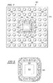
- FIGURE 1 illustrates a bottom plan view of an exemplary prior art ball grid array (BGA) integrated circuit package 100.
- Integrated circuit package 100 comprises solder mask 110.
- the shaded portion of FIGURE 1 represents solder mask 110.
- Each of the plurality of circles shown in FIGURE 1 represents a conventional solder ball 120.
- FIGURE 2 illustrates a cross sectional view of the prior art ball grid array (BGA) integrated circuit package 100 shown in FIGURE 1 taken along line A-A.
- integrated circuit package 100 comprises a substrate 210 having portions that form a square opening within the substrate 210 in the center of the integrated circuit package 100.
- the present invention is not limited to the use of a square opening. In other embodiments the opening may have other geometrical forms (e.g., a rectangle).
- An integrated circuit die 220 having a square shape is located within the square opening in substrate 210.
- a lid 230 is placed over integrated circuit die 220 and is soldered into position over integrated circuit die 220 using a solder reflow process.
- Integrated circuit die 220 is wire bonded to metal layers 240 on substrate 210 and encapsulated in a conventional manner with mold compound 250.
- FIGURE 1 illustrates the location of the placement of integrated circuit die 220 in the center of integrated circuit package 100.
- Integrated circuit die 220 is located within the dashed outline of square 130. Proceeding outwardly from the dashed outline of square 130, the dashed outline of square 140 represents the boundary of the square opening within substrate 210.
- FIGURE 1 also illustrates the location of the placement of lid 230 over integrated circuit die 220.
- the solid outline of square 150 represents the boundary of lid 230.
- the portion 160 between the solid outline of square 150 and the interior edge of solder mask 110 represents the location of metal layer 240 on substrate 210 near the edge of the opening in substrate 210.
- mold compound 250 extends through the opening in substrate 210 and covers the sides of integrated circuit die 220.
- Lid 230 is soldered to metal layer 240 with solder 260. If the upper surface of lid 230 is not in contact with the lower surface of integrated circuit die 220 then a cavity 270 is formed between lid 230 and integrated circuit die 220.
- the high temperature weakens solder 260 that fastens lid 230 to metal layers 240.
- the expansion of moisture diffused into cavity 270 causes an increase in vapor pressure within cavity 270.
- the increased vapor pressure may then cause lid 230 to shift or move out of its original position.
- the increased vapor pressure may cause melted solder 260 to ooze out from around lid 230.
- the present invention solves this problem by providing a ball grid array (BGA) integrated circuit package with solder mask vents for venting pressure that may build up within the integrated circuit package.
- BGA ball grid array
- FIGURE 3 illustrates a bottom plan view of an exemplary ball grid array (BGA) integrated circuit package 300 in accordance with the principles of the present invention.
- Integrated circuit package 300 comprises solder mask 310.
- the shaded portion of FIGURE 3 represents solder mask 310.
- Each of the plurality of circles shown in FIGURE 3 represents a conventional solder ball 320.
- FIGURE 4 illustrates a cross sectional view of the ball grid array (BGA) integrated circuit package 300 shown in FIGURE 3 taken along line B-B.
- solder mask 310 is formed having solder mask vents 315.
- integrated circuit package 300 comprises a substrate 410 having portions that form a square opening within the substrate 410 in the center of the integrated circuit package 300.
- the present invention is not limited to the use of a square opening. In other embodiments the opening may have other geometrical forms (e.g., a rectangle).
- An integrated circuit die 420 having a square shape is located within the square opening in substrate 410.
- a lid 430 is placed over integrated circuit die 420 and is soldered into position over integrated circuit die 420 using a solder reflow process.
- Integrated circuit die 420 is wire bonded to metal layers 440 on substrate 410 and encapsulated in a conventional manner with mold compound 450.
- FIGURE 5 illustrates a more detailed view of the central portion of the bottom plan view of the ball grid array (BFA) integrated circuit package 300 shown in FIGURE 3.
- FIGURE 5 illustrates the location of the placement of integrated circuit die 420 in the center of integrated circuit package 300.
- Integrated circuit die 420 is located within the dashed outline of square 330. Proceeding outwardly from the dashed outline of square 330, the solid outline of square 340 represents the boundary of the square opening within substrate 410.
- 4 and 5 solder mask 310 extends up to the boundary 340 of the square opening within substrate 410.
- FIGURE 5 also illustrates the location of the placement of lid 430 over integrated circuit die 420.
- the solid outline of square 350 represents the boundary of lid 430.
- the portions (160a, 160b, 160c, 160d, 160e, 160f, 160g, 160h) under the solid outline of square 350 represent the location of metal layer 440 on substrate 410 near the edge of the opening in substrate 410.
- Solder mask 310 is formed having a plurality of solder mask vents 315 that separate metal layer 440 into separate portions 160.
- mold compound 450 extends through the opening in substrate 410 and covers the sides of integrated circuit die 420.
- Lid 430 is soldered to metal layer 440 with solder 460. If the upper surface of lid 430 is not in contact with the lower surface of integrated circuit die 420 then a cavity 470 is formed between lid 430 and integrated circuit die 420. Unlike lid 230 in prior art integrated circuit package 100, lid 430 is not soldered to metal layer 440 in a manner that causes solder 460 to completely seal off cavity 470.
- the solder mask vents 315 of solder mask 310 provide a plurality of vapor pressure vents 480 through solder 460.
- vapor pressure vents 480 through solder 460 prevent vapor pressure from building up in cavity 470 when integrated circuit package 300 is subjected to high temperature.
- the venting of vapor pressure insures that lid 430 is not moved out of its proper position during a surface mount process.
- FIGURE 6 illustrates a flow chart that shows an operation of an advantageous embodiment of a first portion of a method of the present invention for manufacturing an integrated circuit having a soldered lid.
- the steps of the first portion of the method shown in FIGURE 6 are collectively referred to with reference numeral 600.
- a substrate 410 of integrated circuit 300 is provided.
- Substrate 410 has a top surface and a bottom surface.
- Substrate 410 also has portions that form an opening through substrate 410.
- Step 610 Then at least one metal layer 440 is placed on substrate 410.
- Metal layer 440 has portions that form a plurality of electrical conductors.
- Step 620 A solder mask 310 is then deposited over portions of metal layer 440 on the bottom surface of substrate 410.
- Solder mask 310 is formed having a plurality of solder mask vents that form a plurality of metal layer portions 160 of metal layer 440 around the opening on the bottom surface of substrate 410.
- Step 630 The first step a substrate 410 of integrated circuit 300 is provided.
- Step 610 has a top surface and a bottom surface.
- Step 410 also has portions that form an opening through substrate 410.
- Step 610 Then at least one metal layer 440 is placed on substrate 410.
- Metal layer 440 has portions that
- Solder material 260 is then applied over the metal areas of metal layer 440. (Step 640). A lid 430 is then provided that is large enough to cover the opening through substrate 410 when lid 430 is placed adjacent to the opening through substrate 410. Lid 430 has a top surface and a bottom surface. Lid 430 is placed over the solder material 260 on metal layer 440. (Step 650). The integrated circuit assembly is then heated in a reflow oven. (Step 660). The heat from the reflow oven melts the solder material 260 to attach lid 430 to the plurality of metal layer portions 160 of metal layer 440 around the opening on the bottom surface of substrate 410. (Step 670).
- FIGURE 7 illustrates a flow chart that shows an operation of an advantageous embodiment of a second portion of a method of the present invention for manufacturing an integrated circuit having a soldered lid.
- the steps of the second portion of the method shown in FIGURE 7 are collectively referred to with reference numeral 700.
- Step 710 of FIGURE 7 follows step 670 of FIGURE 6.
- the solder mask vents form a plurality of vapor pressure vents 480 through the solder 260 that is used to solder lid 430 to the plurality of metal layer portions 160. (Step 710).
- the vapor pressure vents 480 through the solder 260 prevent an increase in vapor pressure from occurring in cavity 270 between lid 430 and integrated circuit die 420.
- Step 720 There is therefore no increase in vapor pressure in cavity 270 that would (1) shift lid 430 out of its desired soldered position when solder 260 is heated, or (2) cause melted solder 260 to flow around lid 430 when solder 260 is heated.
- Integrated circuit die 420 is then mounted within the opening through substrate 410. (Step 730). Integrated circuit die 420 is then electrically connected to the plurality of electrical conductors of metal layer 440. (Step 740).
- the integrated circuit assembly (comprising substrate 410, integrated circuit die 420, and soldered lid 430) is then placed into a conventional mold (not shown).
- Mold compound is then injected onto the top surface of substrate 410 to seal integrated circuit 300 in a conventional integrated circuit package.
- Step 760 The mold compound is cured and a plurality of solder balls 320 is attached to the bottom surface of substrate 410. (Step 770).
- conductive epoxy can be used instead of solder to attach a lid to an integrated circuit die and substrate.
- solder if a continuous patch of epoxy material is applied, the epoxy will stick to the integrated circuit die, the substrate and the solder mask, and will seal the cavity within the integrated circuit package.
- an increase in vapor pressure caused by heating can cause an epoxied lid to move out of its position in the same manner as that previously described for an integrated circuit having a soldered lid.
- An alternate advantageous embodiment of the invention is capable of venting pressure from an integrated circuit package that is sealed with an epoxied lid.
- epoxy is placed on selected portions of the substrate and on selected portions of the integrated circuit die. The placement of individual portions of epoxy creates one or more vapor pressure vents through the epoxy.
- the vapor pressure vents are capable of venting vapor pressure from an integrated circuit having an epoxied lid in the same manner as that previously described for an integrated circuit having a soldered lid.
- FIGURE 8 illustrates a plan view of a prior art epoxy pattern placed on the surface of an integrated circuit die, substrate, and solder mask before the attachment of an epoxied lid.
- the central square in FIGURE 8 represents the location of an integrated circuit die 810.
- the darkly shaded peripheral portion shown in FIGURE 8 represents the location of solder mask 820.
- the lightly shaded portion of FIGURE 8 that fully covers integrated circuit die 810 and that extends to the location of solder mask 820 represents a prior art epoxy pattern 830.
- FIGURE 9 illustrates a plan view of an epoxy venting pattern of the present invention placed on the surface of an integrated circuit die, substrate, and solder mask before the attachment of an epoxied lid.
- the lightly shaded central square in FIGURE 9 represents the location of an integrated circuit die 910.
- the darkly shaded peripheral portion shown in FIGURE 9 represents the location of solder mask 920.
- the eight (8) lightly shaded portions of FIGURE 9 that extend from solder mask 920 to integrated circuit die 910 represent a partial epoxy pattern 930.
- the eight (8) white portions between each of the eight (8) lightly shaded portions of partial epoxy pattern 930 represent a plurality of vapor pressure vents 940. Mold compound may extend into the plurality of vapor pressure vents 940.
- Applying epoxy in accordance with epoxy pattern 930 will cause the epoxy to provide vapor pressure vents 940 so that the opening in the substrate in which integrated circuit die 910 is located will not be completely sealed off.
- An epoxy lid (not shown in FIGURE 9) is then set in position on the epoxy pattern and the epoxy is cured. Vapor pressure vents 940 will prevent the epoxy lid from completely sealing off the bottom region of integrated circuit die 910 and mold compound.
- the epoxy pattern 930 of the present invention provides vapor pressure vents 940 to vent any increase in vapor pressure within a cavity of the integrated circuit.
- FIGURE 10 illustrates a flow chart that shows an operation of an advantageous embodiment of a method of the present invention for manufacturing an integrated circuit having an epoxied lid.
- the steps of the method shown in FIGURE 10 are collectively referred to with reference numeral 1000.
- the flow chart shown in FIGURE 10 describes the method in general terms.
- a substrate for an integrated circuit is provided.
- the substrate has a top surface and a bottom surface.
- the substrate also has portions that form an opening through the substrate.
- at least one metal layer having electrical conductors is placed on the substrate.
- a tape is then placed across the bottom surface of the opening in the substrate.
- the tape is capable of holding an integrated circuit die. (Step 1020).
- An integrated circuit die (IC die) is then placed within the opening through the substrate and held in place by the tape. (Step 1030). Then the integrated circuit die is wire bonded to the metal layer. Mold compound is then applied to seal and protect the integrated circuit die within the integrated circuit. The mold compound is cured and hardened. Because the mold compound now holds the integrated circuit die is place within the opening in the substrate, the tape is now removed from the bottom of the substrate. (Step 1040).
- Epoxy material is then applied to the bottom of the integrated circuit die.
- the epoxy material is applied in accordance with the epoxy pattern of the present invention in order to form vapor pressure vents through the epoxy material.
- An epoxy lid is then provided that is large enough to cover the opening through the substrate when the epoxy lid is placed adjacent to the opening through the substrate.
- the epoxy lid has a top surface and a bottom surface.
- the epoxy is heated in a reflow oven. The heat from the reflow oven melts and cures the epoxy to attach the epoxy lid to the bottom of the integrated circuit die.
- a plurality of solder balls is attached to the bottom surface of the substrate. (Step 1070).
Landscapes
- Engineering & Computer Science (AREA)
- Manufacturing & Machinery (AREA)
- Microelectronics & Electronic Packaging (AREA)
- Cooling Or The Like Of Semiconductors Or Solid State Devices (AREA)
- Wire Bonding (AREA)
- Encapsulation Of And Coatings For Semiconductor Or Solid State Devices (AREA)
- Electric Connection Of Electric Components To Printed Circuits (AREA)
Applications Claiming Priority (2)
| Application Number | Priority Date | Filing Date | Title |
|---|---|---|---|
| US405529 | 2003-04-02 | ||
| US10/405,529 US7126210B2 (en) | 2003-04-02 | 2003-04-02 | System and method for venting pressure from an integrated circuit package sealed with a lid |
Publications (3)
| Publication Number | Publication Date |
|---|---|
| EP1465249A2 true EP1465249A2 (fr) | 2004-10-06 |
| EP1465249A3 EP1465249A3 (fr) | 2004-10-20 |
| EP1465249B1 EP1465249B1 (fr) | 2007-08-01 |
Family
ID=32850617
Family Applications (1)
| Application Number | Title | Priority Date | Filing Date |
|---|---|---|---|
| EP04251989A Expired - Lifetime EP1465249B1 (fr) | 2003-04-02 | 2004-04-01 | Système et méthode d'aération d'un circuit intégré scellé par un capôt |
Country Status (4)
| Country | Link |
|---|---|
| US (2) | US7126210B2 (fr) |
| EP (1) | EP1465249B1 (fr) |
| JP (1) | JP5265842B2 (fr) |
| DE (1) | DE602004007843D1 (fr) |
Cited By (1)
| Publication number | Priority date | Publication date | Assignee | Title |
|---|---|---|---|---|
| CN103871997A (zh) * | 2012-12-14 | 2014-06-18 | 常熟东南相互电子有限公司 | 封装基板与电子组装体 |
Families Citing this family (19)
| Publication number | Priority date | Publication date | Assignee | Title |
|---|---|---|---|---|
| TWI333249B (en) * | 2004-08-24 | 2010-11-11 | Himax Tech Inc | Sensor package |
| US7528474B2 (en) * | 2005-05-31 | 2009-05-05 | Stats Chippac Ltd. | Stacked semiconductor package assembly having hollowed substrate |
| JP2008091714A (ja) * | 2006-10-03 | 2008-04-17 | Rohm Co Ltd | 半導体装置 |
| US8169067B2 (en) * | 2006-10-20 | 2012-05-01 | Broadcom Corporation | Low profile ball grid array (BGA) package with exposed die and method of making same |
| US7554194B2 (en) * | 2006-11-08 | 2009-06-30 | Amkor Technology, Inc. | Thermally enhanced semiconductor package |
| US7919853B1 (en) * | 2007-11-01 | 2011-04-05 | Amkor Technology, Inc. | Semiconductor package and fabrication method thereof |
| US20100019374A1 (en) * | 2008-07-25 | 2010-01-28 | Stmicroelectronics, Inc. | Ball grid array package |
| TWM382505U (en) * | 2010-01-15 | 2010-06-11 | Cheng Uei Prec Ind Co Ltd | Video device |
| US8522426B2 (en) * | 2010-06-05 | 2013-09-03 | Raytheon Company | Vent blocking on vented ball grid arrays to provide a cleaner solution barrier |
| US8906747B2 (en) | 2012-05-23 | 2014-12-09 | Freescale Semiconductor, Inc. | Cavity-type semiconductor package and method of packaging same |
| CN103904062B (zh) * | 2012-12-28 | 2017-04-26 | 欣兴电子股份有限公司 | 内埋式电子元件封装结构 |
| US8736033B1 (en) * | 2013-03-13 | 2014-05-27 | Unimicron Technology Corp. | Embedded electronic device package structure |
| KR101973425B1 (ko) * | 2015-05-11 | 2019-09-02 | 삼성전자주식회사 | 전자부품 패키지 및 그 제조방법 |
| US9842789B2 (en) | 2015-05-11 | 2017-12-12 | Samsung Electro-Mechanics Co., Ltd. | Electronic component package and method of manufacturing the same |
| US10143084B2 (en) * | 2016-12-15 | 2018-11-27 | Nxp Usa, Inc. | Plated opening with vent path |
| KR102724914B1 (ko) * | 2018-12-04 | 2024-11-01 | 삼성전기주식회사 | 전자소자 내장 인쇄회로기판 |
| EP3905861A1 (fr) * | 2020-04-30 | 2021-11-03 | ZKW Group GmbH | Barrière contre le décalage des composants smt |
| US20230290715A1 (en) * | 2022-03-09 | 2023-09-14 | Novatek Microelectronics Corp. | Compact ball grid array package for use in touch panel controller and touch panel device utilizing the same |
| US20250149429A1 (en) * | 2023-11-08 | 2025-05-08 | Amkor Technology Singapore Holding Pte. Ltd. | Electronic devices and methods of manufacturing electronic devices |
Family Cites Families (35)
| Publication number | Priority date | Publication date | Assignee | Title |
|---|---|---|---|---|
| US5612576A (en) * | 1992-10-13 | 1997-03-18 | Motorola | Self-opening vent hole in an overmolded semiconductor device |
| US5474958A (en) | 1993-05-04 | 1995-12-12 | Motorola, Inc. | Method for making semiconductor device having no die supporting surface |
| US5397921A (en) * | 1993-09-03 | 1995-03-14 | Advanced Semiconductor Assembly Technology | Tab grid array |
| US5991156A (en) * | 1993-12-20 | 1999-11-23 | Stmicroelectronics, Inc. | Ball grid array integrated circuit package with high thermal conductivity |
| US5642261A (en) * | 1993-12-20 | 1997-06-24 | Sgs-Thomson Microelectronics, Inc. | Ball-grid-array integrated circuit package with solder-connected thermal conductor |
| US5663106A (en) * | 1994-05-19 | 1997-09-02 | Tessera, Inc. | Method of encapsulating die and chip carrier |
| US5798909A (en) * | 1995-02-15 | 1998-08-25 | International Business Machines Corporation | Single-tiered organic chip carriers for wire bond-type chips |
| US5721450A (en) * | 1995-06-12 | 1998-02-24 | Motorola, Inc. | Moisture relief for chip carriers |
| US5842275A (en) * | 1995-09-05 | 1998-12-01 | Ford Motor Company | Reflow soldering to mounting pads with vent channels to avoid skewing |
| US5843808A (en) * | 1996-01-11 | 1998-12-01 | Asat, Limited | Structure and method for automated assembly of a tab grid array package |
| JPH09232368A (ja) * | 1996-02-20 | 1997-09-05 | Fujitsu Ltd | 半導体装置 |
| CA2180807C (fr) * | 1996-07-09 | 2002-11-05 | Lynda Boutin | Boitier de puce de circuit integre et methode d'encapsulation connexe |
| JP2930057B2 (ja) * | 1997-06-06 | 1999-08-03 | 日本電気株式会社 | Bga型半導体装置 |
| US5900669A (en) * | 1997-06-30 | 1999-05-04 | Motorola, Inc. | Semiconductor component |
| JPH11186294A (ja) * | 1997-10-14 | 1999-07-09 | Sumitomo Metal Smi Electron Devices Inc | 半導体パッケージ及びその製造方法 |
| JP2991172B2 (ja) * | 1997-10-24 | 1999-12-20 | 日本電気株式会社 | 半導体装置 |
| JP3147053B2 (ja) * | 1997-10-27 | 2001-03-19 | 日本電気株式会社 | 樹脂封止型ボールグリッドアレイicパッケージ及びその製造方法 |
| JPH11163022A (ja) * | 1997-11-28 | 1999-06-18 | Sony Corp | 半導体装置、その製造方法及び電子機器 |
| JPH11251480A (ja) * | 1998-03-04 | 1999-09-17 | Toshiba Corp | 半導体パッケージ |
| JP2000150730A (ja) | 1998-11-17 | 2000-05-30 | Fujitsu Ltd | 半導体装置及びその製造方法 |
| US6396136B2 (en) * | 1998-12-31 | 2002-05-28 | Texas Instruments Incorporated | Ball grid package with multiple power/ground planes |
| US6424033B1 (en) * | 1999-08-31 | 2002-07-23 | Micron Technology, Inc. | Chip package with grease heat sink and method of making |
| US6356452B1 (en) * | 1999-10-13 | 2002-03-12 | Micron Technology, Inc. | Soldermask opening to prevent delamination |
| US6338985B1 (en) * | 2000-02-04 | 2002-01-15 | Amkor Technology, Inc. | Making chip size semiconductor packages |
| US6678167B1 (en) * | 2000-02-04 | 2004-01-13 | Agere Systems Inc | High performance multi-chip IC package |
| TW445558B (en) * | 2000-04-14 | 2001-07-11 | Via Tech Inc | Manufacturing method for cavity-down plastic ball grid array package substrate |
| US6278613B1 (en) * | 2000-09-27 | 2001-08-21 | St Assembly Test Services Pte Ltd | Copper pads for heat spreader attach |
| JP3827520B2 (ja) * | 2000-11-02 | 2006-09-27 | 株式会社ルネサステクノロジ | 半導体装置 |
| TW457663B (en) * | 2000-11-08 | 2001-10-01 | Advanced Semiconductor Eng | Substrate structure of heat spreader and its package |
| US7132744B2 (en) * | 2000-12-22 | 2006-11-07 | Broadcom Corporation | Enhanced die-up ball grid array packages and method for making the same |
| TW484195B (en) * | 2001-01-18 | 2002-04-21 | Siliconware Precision Industries Co Ltd | Processing method for grounding solder structure of tape ball grid array package structure |
| US6853070B2 (en) * | 2001-02-15 | 2005-02-08 | Broadcom Corporation | Die-down ball grid array package with die-attached heat spreader and method for making the same |
| US6707163B2 (en) * | 2001-04-13 | 2004-03-16 | Stmicroelectronics, Inc. | Method of eliminating uncontrolled voids in sheet adhesive layer |
| US6580174B2 (en) * | 2001-09-28 | 2003-06-17 | Intel Corporation | Vented vias for via in pad technology yield improvements |
| US6838309B1 (en) * | 2002-03-13 | 2005-01-04 | Amkor Technology, Inc. | Flip-chip micromachine package using seal layer |
-
2003
- 2003-04-02 US US10/405,529 patent/US7126210B2/en not_active Expired - Lifetime
-
2004
- 2004-03-31 JP JP2004106820A patent/JP5265842B2/ja not_active Expired - Lifetime
- 2004-04-01 DE DE602004007843T patent/DE602004007843D1/de not_active Expired - Lifetime
- 2004-04-01 EP EP04251989A patent/EP1465249B1/fr not_active Expired - Lifetime
-
2006
- 2006-09-08 US US11/517,879 patent/US7534716B2/en not_active Expired - Lifetime
Cited By (2)
| Publication number | Priority date | Publication date | Assignee | Title |
|---|---|---|---|---|
| CN103871997A (zh) * | 2012-12-14 | 2014-06-18 | 常熟东南相互电子有限公司 | 封装基板与电子组装体 |
| CN103871997B (zh) * | 2012-12-14 | 2017-05-03 | 常熟东南相互电子有限公司 | 电子组装体 |
Also Published As
| Publication number | Publication date |
|---|---|
| US7534716B2 (en) | 2009-05-19 |
| EP1465249A3 (fr) | 2004-10-20 |
| JP5265842B2 (ja) | 2013-08-14 |
| US7126210B2 (en) | 2006-10-24 |
| DE602004007843D1 (de) | 2007-09-13 |
| US20040195685A1 (en) | 2004-10-07 |
| US20070001286A1 (en) | 2007-01-04 |
| JP2004312005A (ja) | 2004-11-04 |
| EP1465249B1 (fr) | 2007-08-01 |
Similar Documents
| Publication | Publication Date | Title |
|---|---|---|
| EP1465249B1 (fr) | Système et méthode d'aération d'un circuit intégré scellé par un capôt | |
| JP2991172B2 (ja) | 半導体装置 | |
| EP0684641B1 (fr) | Encapsulage d'un dispositif à semi-conducteur ayant une haute résistance à l'humidité | |
| US6601295B2 (en) | Method of producing chip-type electronic devices | |
| US6922339B2 (en) | Heat dissipating structure of printed circuit board and fabricating method thereof | |
| US6215180B1 (en) | Dual-sided heat dissipating structure for integrated circuit package | |
| US6282094B1 (en) | Ball-grid array integrated circuit package with an embedded type of heat-dissipation structure and method of manufacturing the same | |
| US7482204B2 (en) | Chip packaging process | |
| KR0134296B1 (ko) | 반도체 장치 및 제조 방법 | |
| TWI316740B (en) | Package having exposed integrated circuit device | |
| US7781899B2 (en) | Leadframe having mold lock vent | |
| US8269338B2 (en) | Semiconductor device having improved heat dissipation capabilities | |
| US7388284B1 (en) | Integrated circuit package and method of attaching a lid to a substrate of an integrated circuit | |
| US7312525B2 (en) | Thermally enhanced package for an integrated circuit | |
| US20060292741A1 (en) | Heat-dissipating semiconductor package and fabrication method thereof | |
| CN212392238U (zh) | 半导体设备和电子设备 | |
| EP2057665B1 (fr) | Dispositif semi-conducteur et procede de fabrication d'un dispositif semi-conducteur presentant des capacites de dissipation thermique ameliorees | |
| JPH09326450A (ja) | 半導体装置およびその製造方法 | |
| US8431835B2 (en) | Packaging device for an electronic element and method for making the same | |
| JP2003023126A (ja) | 半導体装置 | |
| CN112151463B (zh) | 用于减少焊料中空隙的在裸片焊盘中有腔的半导体封装 | |
| JPH06125024A (ja) | 半導体装置及びその冷却方法 | |
| KR0156513B1 (ko) | 반도체패키지 | |
| KR100373936B1 (ko) | 파워 모듈 방열 구조 | |
| JP2005079376A (ja) | 半導体パッケージ |
Legal Events
| Date | Code | Title | Description |
|---|---|---|---|
| PUAI | Public reference made under article 153(3) epc to a published international application that has entered the european phase |
Free format text: ORIGINAL CODE: 0009012 |
|
| PUAL | Search report despatched |
Free format text: ORIGINAL CODE: 0009013 |
|
| AK | Designated contracting states |
Kind code of ref document: A2 Designated state(s): AT BE BG CH CY CZ DE DK EE ES FI FR GB GR HU IE IT LI LU MC NL PL PT RO SE SI SK TR |
|
| AX | Request for extension of the european patent |
Extension state: AL HR LT LV MK |
|
| AK | Designated contracting states |
Kind code of ref document: A3 Designated state(s): AT BE BG CH CY CZ DE DK EE ES FI FR GB GR HU IE IT LI LU MC NL PL PT RO SE SI SK TR |
|
| AX | Request for extension of the european patent |
Extension state: AL HR LT LV MK |
|
| 17P | Request for examination filed |
Effective date: 20050414 |
|
| AKX | Designation fees paid |
Designated state(s): DE FR GB IT |
|
| GRAP | Despatch of communication of intention to grant a patent |
Free format text: ORIGINAL CODE: EPIDOSNIGR1 |
|
| GRAS | Grant fee paid |
Free format text: ORIGINAL CODE: EPIDOSNIGR3 |
|
| GRAA | (expected) grant |
Free format text: ORIGINAL CODE: 0009210 |
|
| AK | Designated contracting states |
Kind code of ref document: B1 Designated state(s): DE FR GB IT |
|
| REG | Reference to a national code |
Ref country code: GB Ref legal event code: FG4D |
|
| REF | Corresponds to: |
Ref document number: 602004007843 Country of ref document: DE Date of ref document: 20070913 Kind code of ref document: P |
|
| ET | Fr: translation filed | ||
| PLBE | No opposition filed within time limit |
Free format text: ORIGINAL CODE: 0009261 |
|
| STAA | Information on the status of an ep patent application or granted ep patent |
Free format text: STATUS: NO OPPOSITION FILED WITHIN TIME LIMIT |
|
| 26N | No opposition filed |
Effective date: 20080506 |
|
| PG25 | Lapsed in a contracting state [announced via postgrant information from national office to epo] |
Ref country code: DE Free format text: LAPSE BECAUSE OF FAILURE TO SUBMIT A TRANSLATION OF THE DESCRIPTION OR TO PAY THE FEE WITHIN THE PRESCRIBED TIME-LIMIT Effective date: 20071103 |
|
| PG25 | Lapsed in a contracting state [announced via postgrant information from national office to epo] |
Ref country code: IT Free format text: LAPSE BECAUSE OF NON-PAYMENT OF DUE FEES Effective date: 20080430 |
|
| REG | Reference to a national code |
Ref country code: FR Ref legal event code: PLFP Year of fee payment: 13 |
|
| REG | Reference to a national code |
Ref country code: FR Ref legal event code: PLFP Year of fee payment: 14 |
|
| REG | Reference to a national code |
Ref country code: FR Ref legal event code: PLFP Year of fee payment: 15 |
|
| PGFP | Annual fee paid to national office [announced via postgrant information from national office to epo] |
Ref country code: GB Payment date: 20200323 Year of fee payment: 17 |
|
| GBPC | Gb: european patent ceased through non-payment of renewal fee |
Effective date: 20210401 |
|
| PG25 | Lapsed in a contracting state [announced via postgrant information from national office to epo] |
Ref country code: GB Free format text: LAPSE BECAUSE OF NON-PAYMENT OF DUE FEES Effective date: 20210401 |
|
| PGFP | Annual fee paid to national office [announced via postgrant information from national office to epo] |
Ref country code: FR Payment date: 20230321 Year of fee payment: 20 |