EP1465251A2 - Verfahren zur Herstellung eines metall-keramischen gebondeten Substrates - Google Patents
Verfahren zur Herstellung eines metall-keramischen gebondeten Substrates Download PDFInfo
- Publication number
- EP1465251A2 EP1465251A2 EP04007068A EP04007068A EP1465251A2 EP 1465251 A2 EP1465251 A2 EP 1465251A2 EP 04007068 A EP04007068 A EP 04007068A EP 04007068 A EP04007068 A EP 04007068A EP 1465251 A2 EP1465251 A2 EP 1465251A2
- Authority
- EP
- European Patent Office
- Prior art keywords
- metal
- substrate
- active metal
- producing
- active
- Prior art date
- Legal status (The legal status is an assumption and is not a legal conclusion. Google has not performed a legal analysis and makes no representation as to the accuracy of the status listed.)
- Granted
Links
Images


Classifications
-
- H—ELECTRICITY
- H10—SEMICONDUCTOR DEVICES; ELECTRIC SOLID-STATE DEVICES NOT OTHERWISE PROVIDED FOR
- H10W—GENERIC PACKAGES, INTERCONNECTIONS, CONNECTORS OR OTHER CONSTRUCTIONAL DETAILS OF DEVICES COVERED BY CLASS H10
- H10W40/00—Arrangements for thermal protection or thermal control
- H10W40/20—Arrangements for cooling
- H10W40/25—Arrangements for cooling characterised by their materials
- H10W40/255—Arrangements for cooling characterised by their materials having a laminate or multilayered structure, e.g. direct bond copper [DBC] ceramic substrates
-
- C—CHEMISTRY; METALLURGY
- C04—CEMENTS; CONCRETE; ARTIFICIAL STONE; CERAMICS; REFRACTORIES
- C04B—LIME, MAGNESIA; SLAG; CEMENTS; COMPOSITIONS THEREOF, e.g. MORTARS, CONCRETE OR LIKE BUILDING MATERIALS; ARTIFICIAL STONE; CERAMICS; REFRACTORIES; TREATMENT OF NATURAL STONE
- C04B37/00—Joining burned ceramic articles with other burned ceramic articles or other articles by heating
- C04B37/02—Joining burned ceramic articles with other burned ceramic articles or other articles by heating with metallic articles
- C04B37/023—Joining burned ceramic articles with other burned ceramic articles or other articles by heating with metallic articles characterised by the interlayer used
- C04B37/026—Joining burned ceramic articles with other burned ceramic articles or other articles by heating with metallic articles characterised by the interlayer used consisting of metals or metal salts
-
- C—CHEMISTRY; METALLURGY
- C23—COATING METALLIC MATERIAL; COATING MATERIAL WITH METALLIC MATERIAL; CHEMICAL SURFACE TREATMENT; DIFFUSION TREATMENT OF METALLIC MATERIAL; COATING BY VACUUM EVAPORATION, BY SPUTTERING, BY ION IMPLANTATION OR BY CHEMICAL VAPOUR DEPOSITION, IN GENERAL; INHIBITING CORROSION OF METALLIC MATERIAL OR INCRUSTATION IN GENERAL
- C23F—NON-MECHANICAL REMOVAL OF METALLIC MATERIAL FROM SURFACE; INHIBITING CORROSION OF METALLIC MATERIAL OR INCRUSTATION IN GENERAL; MULTI-STEP PROCESSES FOR SURFACE TREATMENT OF METALLIC MATERIAL INVOLVING AT LEAST ONE PROCESS PROVIDED FOR IN CLASS C23 AND AT LEAST ONE PROCESS COVERED BY SUBCLASS C21D OR C22F OR CLASS C25
- C23F1/00—Etching metallic material by chemical means
- C23F1/10—Etching compositions
- C23F1/14—Aqueous compositions
- C23F1/32—Alkaline compositions
- C23F1/40—Alkaline compositions for etching other metallic material
-
- H—ELECTRICITY
- H05—ELECTRIC TECHNIQUES NOT OTHERWISE PROVIDED FOR
- H05K—PRINTED CIRCUITS; CASINGS OR CONSTRUCTIONAL DETAILS OF ELECTRIC APPARATUS; MANUFACTURE OF ASSEMBLAGES OF ELECTRICAL COMPONENTS
- H05K3/00—Apparatus or processes for manufacturing printed circuits
- H05K3/02—Apparatus or processes for manufacturing printed circuits in which the conductive material is applied to the surface of the insulating support and is thereafter removed from such areas of the surface which are not intended for current conducting or shielding
- H05K3/06—Apparatus or processes for manufacturing printed circuits in which the conductive material is applied to the surface of the insulating support and is thereafter removed from such areas of the surface which are not intended for current conducting or shielding the conductive material being removed chemically or electrolytically, e.g. by photo-etch process
-
- H—ELECTRICITY
- H05—ELECTRIC TECHNIQUES NOT OTHERWISE PROVIDED FOR
- H05K—PRINTED CIRCUITS; CASINGS OR CONSTRUCTIONAL DETAILS OF ELECTRIC APPARATUS; MANUFACTURE OF ASSEMBLAGES OF ELECTRICAL COMPONENTS
- H05K3/00—Apparatus or processes for manufacturing printed circuits
- H05K3/38—Improvement of the adhesion between the insulating substrate and the metal
-
- C—CHEMISTRY; METALLURGY
- C04—CEMENTS; CONCRETE; ARTIFICIAL STONE; CERAMICS; REFRACTORIES
- C04B—LIME, MAGNESIA; SLAG; CEMENTS; COMPOSITIONS THEREOF, e.g. MORTARS, CONCRETE OR LIKE BUILDING MATERIALS; ARTIFICIAL STONE; CERAMICS; REFRACTORIES; TREATMENT OF NATURAL STONE
- C04B2237/00—Aspects relating to ceramic laminates or to joining of ceramic articles with other articles by heating
- C04B2237/02—Aspects relating to interlayers, e.g. used to join ceramic articles with other articles by heating
- C04B2237/12—Metallic interlayers
- C04B2237/125—Metallic interlayers based on noble metals, e.g. silver
-
- C—CHEMISTRY; METALLURGY
- C04—CEMENTS; CONCRETE; ARTIFICIAL STONE; CERAMICS; REFRACTORIES
- C04B—LIME, MAGNESIA; SLAG; CEMENTS; COMPOSITIONS THEREOF, e.g. MORTARS, CONCRETE OR LIKE BUILDING MATERIALS; ARTIFICIAL STONE; CERAMICS; REFRACTORIES; TREATMENT OF NATURAL STONE
- C04B2237/00—Aspects relating to ceramic laminates or to joining of ceramic articles with other articles by heating
- C04B2237/02—Aspects relating to interlayers, e.g. used to join ceramic articles with other articles by heating
- C04B2237/12—Metallic interlayers
- C04B2237/126—Metallic interlayers wherein the active component for bonding is not the largest fraction of the interlayer
-
- C—CHEMISTRY; METALLURGY
- C04—CEMENTS; CONCRETE; ARTIFICIAL STONE; CERAMICS; REFRACTORIES
- C04B—LIME, MAGNESIA; SLAG; CEMENTS; COMPOSITIONS THEREOF, e.g. MORTARS, CONCRETE OR LIKE BUILDING MATERIALS; ARTIFICIAL STONE; CERAMICS; REFRACTORIES; TREATMENT OF NATURAL STONE
- C04B2237/00—Aspects relating to ceramic laminates or to joining of ceramic articles with other articles by heating
- C04B2237/02—Aspects relating to interlayers, e.g. used to join ceramic articles with other articles by heating
- C04B2237/12—Metallic interlayers
- C04B2237/126—Metallic interlayers wherein the active component for bonding is not the largest fraction of the interlayer
- C04B2237/127—The active component for bonding being a refractory metal
-
- C—CHEMISTRY; METALLURGY
- C04—CEMENTS; CONCRETE; ARTIFICIAL STONE; CERAMICS; REFRACTORIES
- C04B—LIME, MAGNESIA; SLAG; CEMENTS; COMPOSITIONS THEREOF, e.g. MORTARS, CONCRETE OR LIKE BUILDING MATERIALS; ARTIFICIAL STONE; CERAMICS; REFRACTORIES; TREATMENT OF NATURAL STONE
- C04B2237/00—Aspects relating to ceramic laminates or to joining of ceramic articles with other articles by heating
- C04B2237/30—Composition of layers of ceramic laminates or of ceramic or metallic articles to be joined by heating, e.g. Si substrates
- C04B2237/32—Ceramic
- C04B2237/34—Oxidic
- C04B2237/343—Alumina or aluminates
-
- C—CHEMISTRY; METALLURGY
- C04—CEMENTS; CONCRETE; ARTIFICIAL STONE; CERAMICS; REFRACTORIES
- C04B—LIME, MAGNESIA; SLAG; CEMENTS; COMPOSITIONS THEREOF, e.g. MORTARS, CONCRETE OR LIKE BUILDING MATERIALS; ARTIFICIAL STONE; CERAMICS; REFRACTORIES; TREATMENT OF NATURAL STONE
- C04B2237/00—Aspects relating to ceramic laminates or to joining of ceramic articles with other articles by heating
- C04B2237/30—Composition of layers of ceramic laminates or of ceramic or metallic articles to be joined by heating, e.g. Si substrates
- C04B2237/32—Ceramic
- C04B2237/36—Non-oxidic
- C04B2237/366—Aluminium nitride
-
- C—CHEMISTRY; METALLURGY
- C04—CEMENTS; CONCRETE; ARTIFICIAL STONE; CERAMICS; REFRACTORIES
- C04B—LIME, MAGNESIA; SLAG; CEMENTS; COMPOSITIONS THEREOF, e.g. MORTARS, CONCRETE OR LIKE BUILDING MATERIALS; ARTIFICIAL STONE; CERAMICS; REFRACTORIES; TREATMENT OF NATURAL STONE
- C04B2237/00—Aspects relating to ceramic laminates or to joining of ceramic articles with other articles by heating
- C04B2237/30—Composition of layers of ceramic laminates or of ceramic or metallic articles to be joined by heating, e.g. Si substrates
- C04B2237/40—Metallic
- C04B2237/407—Copper
-
- C—CHEMISTRY; METALLURGY
- C04—CEMENTS; CONCRETE; ARTIFICIAL STONE; CERAMICS; REFRACTORIES
- C04B—LIME, MAGNESIA; SLAG; CEMENTS; COMPOSITIONS THEREOF, e.g. MORTARS, CONCRETE OR LIKE BUILDING MATERIALS; ARTIFICIAL STONE; CERAMICS; REFRACTORIES; TREATMENT OF NATURAL STONE
- C04B2237/00—Aspects relating to ceramic laminates or to joining of ceramic articles with other articles by heating
- C04B2237/50—Processing aspects relating to ceramic laminates or to the joining of ceramic articles with other articles by heating
- C04B2237/64—Forming laminates or joined articles comprising grooves or cuts
-
- C—CHEMISTRY; METALLURGY
- C04—CEMENTS; CONCRETE; ARTIFICIAL STONE; CERAMICS; REFRACTORIES
- C04B—LIME, MAGNESIA; SLAG; CEMENTS; COMPOSITIONS THEREOF, e.g. MORTARS, CONCRETE OR LIKE BUILDING MATERIALS; ARTIFICIAL STONE; CERAMICS; REFRACTORIES; TREATMENT OF NATURAL STONE
- C04B2237/00—Aspects relating to ceramic laminates or to joining of ceramic articles with other articles by heating
- C04B2237/50—Processing aspects relating to ceramic laminates or to the joining of ceramic articles with other articles by heating
- C04B2237/70—Forming laminates or joined articles comprising layers of a specific, unusual thickness
- C04B2237/704—Forming laminates or joined articles comprising layers of a specific, unusual thickness of one or more of the ceramic layers or articles
-
- C—CHEMISTRY; METALLURGY
- C04—CEMENTS; CONCRETE; ARTIFICIAL STONE; CERAMICS; REFRACTORIES
- C04B—LIME, MAGNESIA; SLAG; CEMENTS; COMPOSITIONS THEREOF, e.g. MORTARS, CONCRETE OR LIKE BUILDING MATERIALS; ARTIFICIAL STONE; CERAMICS; REFRACTORIES; TREATMENT OF NATURAL STONE
- C04B2237/00—Aspects relating to ceramic laminates or to joining of ceramic articles with other articles by heating
- C04B2237/50—Processing aspects relating to ceramic laminates or to the joining of ceramic articles with other articles by heating
- C04B2237/70—Forming laminates or joined articles comprising layers of a specific, unusual thickness
- C04B2237/706—Forming laminates or joined articles comprising layers of a specific, unusual thickness of one or more of the metallic layers or articles
-
- H—ELECTRICITY
- H05—ELECTRIC TECHNIQUES NOT OTHERWISE PROVIDED FOR
- H05K—PRINTED CIRCUITS; CASINGS OR CONSTRUCTIONAL DETAILS OF ELECTRIC APPARATUS; MANUFACTURE OF ASSEMBLAGES OF ELECTRICAL COMPONENTS
- H05K1/00—Printed circuits
- H05K1/02—Details
- H05K1/03—Use of materials for the substrate
- H05K1/0306—Inorganic insulating substrates, e.g. ceramic, glass
-
- H—ELECTRICITY
- H05—ELECTRIC TECHNIQUES NOT OTHERWISE PROVIDED FOR
- H05K—PRINTED CIRCUITS; CASINGS OR CONSTRUCTIONAL DETAILS OF ELECTRIC APPARATUS; MANUFACTURE OF ASSEMBLAGES OF ELECTRICAL COMPONENTS
- H05K2201/00—Indexing scheme relating to printed circuits covered by H05K1/00
- H05K2201/07—Electric details
- H05K2201/0753—Insulation
- H05K2201/0761—Insulation resistance, e.g. of the surface of the PCB between the conductors
-
- H—ELECTRICITY
- H05—ELECTRIC TECHNIQUES NOT OTHERWISE PROVIDED FOR
- H05K—PRINTED CIRCUITS; CASINGS OR CONSTRUCTIONAL DETAILS OF ELECTRIC APPARATUS; MANUFACTURE OF ASSEMBLAGES OF ELECTRICAL COMPONENTS
- H05K2203/00—Indexing scheme relating to apparatus or processes for manufacturing printed circuits covered by H05K3/00
- H05K2203/14—Related to the order of processing steps
- H05K2203/1476—Same or similar kind of process performed in phases, e.g. coarse patterning followed by fine patterning
-
- H—ELECTRICITY
- H05—ELECTRIC TECHNIQUES NOT OTHERWISE PROVIDED FOR
- H05K—PRINTED CIRCUITS; CASINGS OR CONSTRUCTIONAL DETAILS OF ELECTRIC APPARATUS; MANUFACTURE OF ASSEMBLAGES OF ELECTRICAL COMPONENTS
- H05K3/00—Apparatus or processes for manufacturing printed circuits
- H05K3/02—Apparatus or processes for manufacturing printed circuits in which the conductive material is applied to the surface of the insulating support and is thereafter removed from such areas of the surface which are not intended for current conducting or shielding
- H05K3/06—Apparatus or processes for manufacturing printed circuits in which the conductive material is applied to the surface of the insulating support and is thereafter removed from such areas of the surface which are not intended for current conducting or shielding the conductive material being removed chemically or electrolytically, e.g. by photo-etch process
- H05K3/067—Etchants
-
- H—ELECTRICITY
- H05—ELECTRIC TECHNIQUES NOT OTHERWISE PROVIDED FOR
- H05K—PRINTED CIRCUITS; CASINGS OR CONSTRUCTIONAL DETAILS OF ELECTRIC APPARATUS; MANUFACTURE OF ASSEMBLAGES OF ELECTRICAL COMPONENTS
- H05K3/00—Apparatus or processes for manufacturing printed circuits
- H05K3/22—Secondary treatment of printed circuits
- H05K3/26—Cleaning or polishing of the conductive pattern
Definitions
- the present invention generally relates to a method for producing a metal/ceramic bonding substrate. Morespecifically,theinvention relates to a method for producing a metal/ceramic bonding substrate wherein ametal member is bonded to a ceramic substrate via an active metal containing brazing filler metal.
- a typical metal/ceramic bonding substrate used as an insulating substrate cracks are easily produced in a ceramic member by a thermal stress based on the difference in thermal expansion which is caused between the ceramic member and a metal member by thermal shocks after bonding.
- a method for relaxing such a thermal stress there is known a method for thinning the peripheral portion (creeping portion) of a metal member, i.e. a method for forming a stepped structure or a fillet on the peripheral portion of a metal member.
- a method for forming a fillet on the peripheral portion of a metal circuit by steps of: printing a resist on a predetermined portion of a surface of a metal plate bonded to a ceramic member via an active metal containing brazing filler metal; etching unnecessary part of the metal plate to form metal circuits, and then, removing the resist; removing unnecessary part of the brazing filler metal remaining between the metal circuits; printing a resist on the surface of the metal circuits again to etch unnecessary part of the metal circuits again; and removing the resist, i.e., by carrying out a circuit pattern printing process and a metal circuit etching process twice, respectively.
- a layer which is mainly formed of a metal other than an active metal of the active metal containing brazing filler metal, of two layers formed of the active metal containing brazing filler metal, i.e., the metal layer and a layer (which will be hereinafter referred to as an "active metal layer") which is mainly formed of the active metal and its compound(s), may be excessively etched (side-etched), so that there are some cases where it is difficult to form the fillet.
- the etchant containing the inorganic acid and hydrofluoric acid is easy to damage ceramics, so that there are some cases where reliability, such as heat cycle resistance, may be deteriorated.
- the inventor has diligently studied and found that it is possible to form a fillet on the peripheral portion of a metal circuit by a small number of steps to produce a reliable metal/ceramic bonding substrate at low costs, by etching an active metal layer of an active metal containing brazing filler metal while inhibiting excessive etching (side etching) of a metal layer, which is formed of a metal other than the active metal of the brazing filler metal, into the metal circuit by using a chemical, which inhibits the metal circuit and the metal layer of the brazing filler metal from being etched and which selectively etch the active metal layer, when the active metal layer of the brazing filler metal is removed after a part of the metal layer is etched with a chemical.
- etching an active metal layer of an active metal containing brazing filler metal while inhibiting excessive etching (side etching) of a metal layer, which is formed of a metal other than the active metal of the brazing filler metal, into the metal circuit by using a chemical, which inhibits
- a method for producing a metal/ceramic bonding substrate wherein a metal member is bonded to at least one side of a ceramic substrate via an active metal containing brazing filler metal comprising the steps of: bonding a metal member to at least one side of a ceramic substrate via an active metal containing brazing filler metal; applying a resist on a predetermined portion of a surface of the metal member to etch a part of the metal member, and then, removing the resist; etching a part of a metal layer, which is mainly formed of a metal other than an active metal of the active metal containing brazing filler metal, with a chemical; and selectively etching a part of an active metal layer, which is formed of the active metal and a compound thereof, with a chemical which inhibits the metal member and the metal layer from being etched and which selectively etch the active metal layer, to form a metal circuit on the ceramic substrate.
- This method for producing a metal/ceramic bonding substrate may further comprise a step of forming a fillet on a peripheral portion of the metal circuit by chemically polishing the metal circuit after selectively etching the part of the active metal layer of the active metal containing brazing filler metal.
- the fillet preferably has a width of 30 ⁇ m or more.
- the active metal containing brazing filler metal is preferably arranged in a region which includes a metal circuit forming region for forming the metal circuit on the ceramic substrate and which is wider than the metal circuit forming region.
- the metal other than the active metal of the active metal containing brazing filler metal is preferably at least one kind of metal selected from the group consisting of silver, copper, nickel, tin, zinc and indium.
- the active metal of the active metal containing brazing filler metal is preferably at least one kind of metal selected from the group consisting of titanium, zirconium and hafnium.
- the chemical for selectively etching the active metal layer preferably contains a compound forming a complex with the active metal, an oxidizer and an alkali.
- the alkali is preferably one selected from the group consisting of ammonia, sodium hydroxide and potassium hydroxide, or a material being alkaline when it is dissolved in water.
- the compound forming a complex with the active metal is preferably an acidic compound.
- the acidic compound may be a carboxylic acid type compound.
- the acidic compound is preferably one selected from the group consisting of citric acid, diethylenetriaminepentaacetic acid (DTPA), ethylenediaminetetraacetic acid (EDTA), hydroxyethylethylenediaminetriacetic acid (HEDTA), 1,3-propanediaminetriacetic acid (1,3PDTA), nitrilotriacetic acid (NTA) and hydroxyethylidenediphosphoric acid (HEDT).
- DTPA diethylenetriaminepentaacetic acid
- EDTA ethylenediaminetetraacetic acid
- HEDTA hydroxyethylethylenediaminetriacetic acid
- 1,3PDTA 1,3-propanediaminetriacetic acid
- NTA nitrilotriacetic acid
- HEDT hydroxyethylidenediphosphoric acid
- the chemical for selectively etching the active metal layer may contain a compound forming a complex with the active metal, an oxidizer and an acid.
- the acid is preferably one selected from the group consisting of hydrochloric acid, sulfuric acid and nitric acid.
- the compound forming a complex with the active metal is preferably an alkaline compound.
- the alkaline compound may be a compound having at least one amino group in its molecule.
- the alkaline compound is preferably ethylenediamine.
- the oxidizer is preferably one selected from the group consisting of hydrogen peroxide, potassium dichromate and potassium permanganate.
- agitation such as oscillation, convection of liquid, bubbling, or application of ultrasonic wave, is preferably carried out at the step of selectively etching the part of the active metal layer of the active metal containing brazing filler metal.
- all or part of a surface of the metal circuit is preferably plated with nickel or a nickel alloy.
- the present invention it is possible to form a desired fillet while preventing side etching and while decreasing damage to a ceramic, by using an etchant, which is capable of inhibiting etching of a metal layer while selectively removing only an active metal layer, if only a copper circuit printing step and a copper circuit etching step are carried out once, respectively.
- an etchant which is capable of inhibiting etching of a metal layer while selectively removing only an active metal layer, if only a copper circuit printing step and a copper circuit etching step are carried out once, respectively.
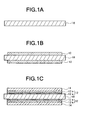
- a ceramic substrate 10 is prepared (FIG. 1A), and a paste-like active metal containing brazing filler metal 12 is printed on both sides of the ceramic substrate 10 by screen printing (FIG. 1B). Then, a metal member 14 is arranged on the brazing filler metal 12 on both sides of the ceramic substrate 10 to be heated in substantially vacuum or non-oxidizing atmosphere. Thereafter, they are cooled to bond the metal member 14 to both sides of the ceramic substrate 10.
- the active metal containing brazing filler metal 12 forms a layer (active metal layer) 12a, which is mainly formed of an active metal of the active metal containing brazing filler metal and its compound(s), and a layer (metal layer) 12b which is mainly formed of a metal other than the active metal of the active metal containing brazing filler metal (FIG. 1C).
- the layers 12a and 12b are not always layers which are clearly separated as shown in the figure. There are some cases where the boundary between the layers 12a and 12b may be clearly observed to some extent, or there are some cases where the layers 12a and 12b may be apparently observed as a single layer in accordance with the kind and thickness of the brazing filler metal and other conditions.
- the active metal containing brazing filler metal 12 may be a foil or a film formed by sputtering.
- a substrate of an oxide mainly containing alumina or silica, or a non-oxide mainly containing aluminum nitride or silicon nitride or silicon carbonate, having a size of about 5 to 200 mm x 5 to 200 mm x 0.25 to 3.0 mm, may be used.
- a metal foil or plate of a simple metal, such as copper, aluminum or nickel, a copper alloy, such as manganin or brass, or an alloy, such as stainless, having a thickness of 0.1 to 0.5 mm, may be used.
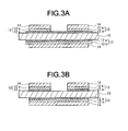
- a resist 16 having a desired circuit pattern is printed on the bonded metal member 14 on both sides (FIG. 2A) , and unnecessary part of the metal member 14 is etched and removed with an etchant of cupric chloride or iron chloride (FIG. 2B) to remove the resist 16 (FIG. 2C).
- the resist 16 may be formed by another method, such as dry film.
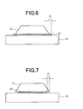
- the width of the fillet can be flexibly controlled to be in the range of, e.g., from 0 to 250 ⁇ m, by changing the chemical polishing solution and processing time.
- the width of the fillet means a length shown by D in FIG. 6.
- the sides of the metal member are shown to be perpendicular to the ceramic substrate in FIGS. 1C through 4B, the sides of the metal member are obliquely shown in FIG. 6. These figures are schematically shown, and the sides of the metal member are etched in fact, so that the sides of the metal member are often inclined as shown in the figures or have a circular shape.
- the chemical used for removing the unnecessary part of the active metal layer 12a may be a chemical containing: a carboxylic acid type compound forming a complex with an active metal, such as titanium, zirconium or hafnium, or a compound having at least one amino group in its molecule; an oxidizer, such as hydrogen peroxide, potassium dichromate or potassium permanganate; and an acid or alkali to be added for causing the complex to be water soluble.
- the acid or alkali may be selected in accordance with the compound forming the complex with the active metal.
- an alkali such as ammonia, sodium hydroxide or potassium hydroxide, is used.
- pH of the chemical is preferably in the range of from 7 to 10, and more preferably in the range of from 8.5 to 9.5. If pH exceeds 10, the solution is decomposed, and if pH is lower than 7, it is difficult to dissolve the acidic compound.
- an alkaline compound such as an amine compound
- an acid such as hydrochloric acid, sulfuric acid or nitric acid, is used.
- unnecessary part of a metal layer (a layer of a metal other than the active metal of the active metal containing brazing filler metal) and a part of unnecessary part of the active metal layer mainly containing titanium nitride, which had remained between copper circuits and on the end portion of the aluminum nitride substrate, were etched and removed at 20 °C for 15 minutes with a solution containing 5% of hydrogen peroxide, 3% of aqueous ammonia and 1.6 wt% of EDTA. After this etching, the substrate was observed with naked eyes. As a result, there was no gap between the copper circuit and the aluminum nitride substrate, and no side etch was confirmed.
- unnecessary part of a metal layer (a layer of a metal other than an active metal of the active metal containing brazing filler metal) and a part of unnecessary part of the active metal layer mainly containing titanium nitride, which had remained between copper circuits and on the end portion of the aluminum nitride substrate, were etched and removed at 20 °C for 15 minutes with a solution containing 5% of hydrogen peroxide, 3% of aqueous ammonia and 1.6 wt% of EDTA. After this etching, the substrate was observed with naked eyes. As a result, there was no gap between the copper circuit and the aluminum nitride substrate, and no side etch was confirmed.
- a chemical containing 3% of ethylenediamine, 5% of potassium permanganate and 3.8% of hydrochloric acid was used as an etchant for selectively etching unnecessary part of an active metal layer, and that the chemical polishing time was 4 minutes.
- hafnium hafnium
- a chemical containing 3% of EDTA ⁇ 4Na and 4% of potassium dichromate was used as an etchant for selectively etching unnecessary part of an active metal layer, and that the chemical polishing time was 4 minutes.
- the substrate was observed with naked eyes. As a result, it was observed that there was a gap between the copper circuit and the alumina substrate.
- a chemical containing 2% of HEDTA ⁇ 3Na and 5% of hydrogen peroxide was used as an etchant for selectively etching unnecessary part of an active metal layer, and that the chemical polishing time was 5 minutes and 30 seconds.
- the substrate was observed with naked eyes. As a result, it was observed that there was a gap between the copper circuit and the alumina substrate.
- a chemical containing 3% of 3PDTA, 7% of hydrogen peroxide and 1.8% of sodium hydroxide was used as an etchant for selectively etching unnecessary part of an active metal layer.
- the substrate was observed with naked eyes. As a result, it was observed that there was a gap between the copper circuit and the alumina substrate.
- a chemical containing 2% of citric acid, 9% of hydrogen peroxide and 1.8% of potassium hydroxide was used as an etchant for selectively etching unnecessary part of an active metal layer at 37 °C for 60 minutes, and that the chemical polishing time was 4 minutes.
- a metal/ceramic bonding substrate was produced by the same method as that in Example 7, except that a chemical containing 1.8% of DTPA ⁇ 5Na and 6% of hydrogen peroxide was used as an etchant for selectively etching unnecessary part of an active metal layer.
- a chemical containing 1.8% of DTPA ⁇ 5Na and 6% of hydrogen peroxide was used as an etchant for selectively etching unnecessary part of an active metal layer.
- hydrochloric acid a chemical containing 1.5% of ethylenediamine, 5% of potassium permanganate and 2% of hydrochloric acid was used as an etchant for selectively etching unnecessary part of an active metal layer.
- a chemical containing 2% of EDTA ⁇ 4Na and 4% of potassium dichromate was used as an etchant for selectively etching unnecessary part of an active metal layer.
- a chemical containing 2% of NTA ⁇ 3Na and 5% of hydrogen peroxide was used as an etchant for selectively etching unnecessary part of an active metal layer, and that the chemical polishing time was 5 minutes.
- a chemical containing 1.5% of 3PDTA, 7% of hydrogen peroxide and 1.0% of sodium hydroxide was used as an etchant for selectively etching unnecessary part of an active metal layer, and that the chemical polishing time was 5 minutes.
- a metal/ceramic bonding substrate was produced by the same method as that in Example 7, except that a chemical containing 1.8% of HEDTA ⁇ 3Na and 8% of hydrogen peroxide was used as an etchant for selectively etching unnecessary part of an active metal layer.
- a chemical containing 1.8% of HEDTA ⁇ 3Na and 8% of hydrogen peroxide was used as an etchant for selectively etching unnecessary part of an active metal layer.
- a metal/ceramic bonding substrate was produced by the same method as that in Example 7, except that a chemical containing 1.8% of HEDP. 4Na and 8% of hydrogen peroxide was used as an etchant for selectively etching unnecessary part of an active metal layer.
- a chemical containing 1.8% of HEDP. 4Na and 8% of hydrogen peroxide was used as an etchant for selectively etching unnecessary part of an active metal layer.
- unnecessary part of a metal layer a layer of a metal other than the active metal of the active metal containing brazing filler metal
- a part of unnecessary part of the active metal layer which had remained between copper circuits and on the end portion of the aluminum nitride substrate, were removed by etching, the substrate was observed with naked eyes. As a result, there was no gap between the copper circuit and the aluminum nitride substrate, and no side etch was confirmed.
- a metal/ceramic bonding substrate was produced by the same method as that in Example 7, except that a chemical containing 2% of DTPA ⁇ 5Na and 7% of hydrogen peroxide was used as an etchant for selectively etching unnecessary part of an active metal layer.
- a chemical containing 2% of DTPA ⁇ 5Na and 7% of hydrogen peroxide was used as an etchant for selectively etching unnecessary part of an active metal layer.
- a metal/ceramic bonding substrate was produced by the same method as that in Comparative Example 2, except that unnecessary part of the brazing filler metal remaining between copper circuits and on the end portion of the aluminum nitride substrate was etched and removed at 20 °C for 45 minutes with a solution containing 5% of hydrogen peroxide, 3% of aqueous ammonia and 1.6 wt% of EDTA.
- the substrate was observed with naked eyes. As a result, it was observed that there was a gap between the copper circuit and the aluminum nitride substrate.
- the substrate was observed with naked eyes. As a result, it was observed that there was a gap between the copper circuit and the aluminum nitride substrate.
Landscapes
- Engineering & Computer Science (AREA)
- Chemical & Material Sciences (AREA)
- Ceramic Engineering (AREA)
- Manufacturing & Machinery (AREA)
- Microelectronics & Electronic Packaging (AREA)
- Materials Engineering (AREA)
- Organic Chemistry (AREA)
- Structural Engineering (AREA)
- Chemical Kinetics & Catalysis (AREA)
- General Chemical & Material Sciences (AREA)
- Mechanical Engineering (AREA)
- Metallurgy (AREA)
- Manufacturing Of Printed Circuit Boards (AREA)
- Ceramic Products (AREA)
- ing And Chemical Polishing (AREA)
- Manufacturing Of Printed Wiring (AREA)
Applications Claiming Priority (6)
| Application Number | Priority Date | Filing Date | Title |
|---|---|---|---|
| JP2003086957 | 2003-03-27 | ||
| JP2003086957 | 2003-03-27 | ||
| JP2003183844 | 2003-06-27 | ||
| JP2003183844 | 2003-06-27 | ||
| JP2004049135A JP4394477B2 (ja) | 2003-03-27 | 2004-02-25 | 金属−セラミックス接合基板の製造方法 |
| JP2004049135 | 2004-02-25 |
Publications (3)
| Publication Number | Publication Date |
|---|---|
| EP1465251A2 true EP1465251A2 (de) | 2004-10-06 |
| EP1465251A3 EP1465251A3 (de) | 2009-09-09 |
| EP1465251B1 EP1465251B1 (de) | 2019-01-23 |
Family
ID=32854121
Family Applications (1)
| Application Number | Title | Priority Date | Filing Date |
|---|---|---|---|
| EP04007068.2A Expired - Lifetime EP1465251B1 (de) | 2003-03-27 | 2004-03-24 | Verfahren zur Herstellung eines metall-keramischen gebondeten Substrates |
Country Status (4)
| Country | Link |
|---|---|
| US (1) | US7219826B2 (de) |
| EP (1) | EP1465251B1 (de) |
| JP (1) | JP4394477B2 (de) |
| HU (1) | HUE043119T2 (de) |
Cited By (5)
| Publication number | Priority date | Publication date | Assignee | Title |
|---|---|---|---|---|
| EP1699080B1 (de) * | 2005-03-04 | 2011-05-18 | Dowa Metaltech Co., Ltd. | Keramiksubstrat und seine Herstellung |
| EP2109138A4 (de) * | 2006-12-26 | 2012-02-22 | Kyocera Corp | Wärmeabführendes substrat und elektronische anordnung damit |
| CN107135608A (zh) * | 2016-02-26 | 2017-09-05 | 住友金属矿山株式会社 | 叠层体的蚀刻方法和使用了其的印刷配线基板的制造方法 |
| EP3370488A1 (de) * | 2017-03-03 | 2018-09-05 | Dowa Metaltech Co., Ltd. | Verfahren zur herstellung einer metall/keramik-leiterplatte |
| EP3321957A4 (de) * | 2015-07-09 | 2019-03-27 | Kabushiki Kaisha Toshiba | Keramik-metall-leiterplatte und halbleiterbauelement damit |
Families Citing this family (49)
| Publication number | Priority date | Publication date | Assignee | Title |
|---|---|---|---|---|
| DE10144269A1 (de) * | 2001-09-08 | 2003-03-27 | Bosch Gmbh Robert | Sensorelement zur Erfassung einer physikalischen Messgröße zwischen tribologisch hoch beanspruchten Körpern |
| JP3863067B2 (ja) * | 2002-06-04 | 2006-12-27 | Dowaホールディングス株式会社 | 金属−セラミックス接合体の製造方法 |
| EP1394528A3 (de) * | 2002-08-13 | 2005-11-16 | Csir | Vorrichtung zur Entnahme einer Stoffprobe in einer Gas |
| JP4014528B2 (ja) * | 2003-03-28 | 2007-11-28 | 日本碍子株式会社 | ヒートスプレッダモジュールの製造方法及びヒートスプレッダモジュール |
| JP4930833B2 (ja) * | 2006-12-11 | 2012-05-16 | 日立金属株式会社 | セラミックス回路基板およびその製造方法 |
| DE102007029031A1 (de) * | 2007-06-23 | 2008-12-24 | Fraunhofer-Gesellschaft zur Förderung der angewandten Forschung e.V. | Verfahren zum dauerhaften Verbinden zweier Komponenten durch Löten mit Glas- oder Metalllot |
| US8663484B2 (en) * | 2007-07-09 | 2014-03-04 | Sumitomo Metal Mining Co., Ltd. | Method for manufacturing a printed circuit board and a printed circuit board obtained by the manufacturing method |
| CN101690429B (zh) * | 2007-09-10 | 2013-09-11 | 住友金属矿山株式会社 | 印刷布线基板的制造方法及由该制造方法所得的印刷布线基板 |
| DE102009000514A1 (de) * | 2009-01-30 | 2010-08-26 | Robert Bosch Gmbh | Verbundbauteil sowie Verfahren zum Herstellen eines Verbundbauteil |
| WO2010113892A1 (ja) * | 2009-03-30 | 2010-10-07 | 株式会社トクヤマ | メタライズド基板を製造する方法、メタライズド基板 |
| JP2011077364A (ja) * | 2009-09-30 | 2011-04-14 | Hitachi Cable Ltd | プリント配線基板の製造方法及びその製造装置 |
| US9096471B2 (en) * | 2009-11-27 | 2015-08-04 | Showa Denko K.K. | Method for producing a layered material |
| US9374893B2 (en) | 2010-03-02 | 2016-06-21 | Tokuyama Corporation | Production method of metallized substrate |
| CN102335793B (zh) * | 2010-07-22 | 2016-11-23 | 江苏道康发电机组有限公司 | 不锈钢与氧化铝陶瓷的连接方法 |
| JP5743503B2 (ja) * | 2010-11-29 | 2015-07-01 | 京セラ株式会社 | ろう材およびこれを用いた回路基板ならびに電子装置 |
| JP5752504B2 (ja) * | 2011-06-30 | 2015-07-22 | 株式会社トクヤマ | 配線基板のめっき方法、めっき配線基板の製造方法、及び銀エッチング液 |
| US10105795B2 (en) * | 2012-05-25 | 2018-10-23 | General Electric Company | Braze compositions, and related devices |
| JP6111764B2 (ja) * | 2013-03-18 | 2017-04-12 | 三菱マテリアル株式会社 | パワーモジュール用基板の製造方法 |
| JP5672324B2 (ja) * | 2013-03-18 | 2015-02-18 | 三菱マテリアル株式会社 | 接合体の製造方法及びパワーモジュール用基板の製造方法 |
| EP3041045B1 (de) * | 2013-08-26 | 2019-09-18 | Mitsubishi Materials Corporation | Verbundkörper und leistungsmodulsubstrat |
| JP6079505B2 (ja) * | 2013-08-26 | 2017-02-15 | 三菱マテリアル株式会社 | 接合体及びパワーモジュール用基板 |
| EP2916627B1 (de) | 2013-08-29 | 2019-04-03 | Hitachi Metals, Ltd. | Verfahren zur herstellung einer keramischen leiterplatte |
| WO2015125907A1 (ja) * | 2014-02-21 | 2015-08-27 | 電気化学工業株式会社 | セラミックス回路基板 |
| JP6256176B2 (ja) * | 2014-04-25 | 2018-01-10 | 三菱マテリアル株式会社 | 接合体の製造方法、パワーモジュール用基板の製造方法 |
| JP6400422B2 (ja) * | 2014-10-07 | 2018-10-03 | Dowaメタルテック株式会社 | 金属−セラミックス回路基板およびその製造方法 |
| US9548518B2 (en) * | 2014-12-16 | 2017-01-17 | General Electric Company | Methods for joining ceramic and metallic structures |
| KR101856106B1 (ko) * | 2015-04-24 | 2018-05-09 | 주식회사 아모센스 | 세라믹 기판 제조 방법 및 이 제조방법으로 제조된 세라믹 기판 |
| KR101856108B1 (ko) * | 2015-04-24 | 2018-05-09 | 주식회사 아모센스 | 세라믹 기판 제조 방법 및 이 제조방법으로 제조된 세라믹 기판 |
| KR101856109B1 (ko) * | 2015-04-24 | 2018-05-09 | 주식회사 아모센스 | 세라믹 기판 제조 방법 및 이 제조방법으로 제조된 세라믹 기판 |
| KR101856107B1 (ko) * | 2015-04-24 | 2018-05-09 | 주식회사 아모센스 | 세라믹 기판 제조 방법 및 이 제조방법으로 제조된 세라믹 기판 |
| CN107889559B (zh) | 2015-04-24 | 2020-04-28 | 阿莫善斯有限公司 | 陶瓷基板的制造方法及由其所制造的陶瓷基板 |
| JP6819299B2 (ja) * | 2016-01-22 | 2021-01-27 | 三菱マテリアル株式会社 | 接合体、パワーモジュール用基板、接合体の製造方法及びパワーモジュール用基板の製造方法 |
| WO2017126641A1 (ja) * | 2016-01-22 | 2017-07-27 | 三菱マテリアル株式会社 | 接合体、パワーモジュール用基板、接合体の製造方法及びパワーモジュール用基板の製造方法 |
| US10252371B2 (en) | 2016-02-12 | 2019-04-09 | The Boeing Company | Diffusion-bonded metallic materials |
| US9682445B1 (en) * | 2016-02-12 | 2017-06-20 | The Boeing Company | Diffusion-bonded metallic materials |
| JP6631333B2 (ja) * | 2016-03-11 | 2020-01-15 | 三菱マテリアル株式会社 | パワーモジュール用基板の製造方法 |
| JP6904094B2 (ja) * | 2016-06-23 | 2021-07-14 | 三菱マテリアル株式会社 | 絶縁回路基板の製造方法 |
| JP2018121014A (ja) * | 2017-01-27 | 2018-08-02 | 三菱マテリアル株式会社 | 絶縁回路基板の製造方法 |
| WO2018221492A1 (ja) | 2017-05-30 | 2018-12-06 | デンカ株式会社 | セラミックス回路基板及びその製造方法 |
| WO2019022133A1 (ja) | 2017-07-25 | 2019-01-31 | デンカ株式会社 | セラミックス回路基板及びその製造方法 |
| WO2019054294A1 (ja) * | 2017-09-12 | 2019-03-21 | 株式会社 東芝 | セラミックス回路基板の製造方法 |
| JP2020010004A (ja) * | 2018-07-12 | 2020-01-16 | Koa株式会社 | 抵抗器及び回路基板 |
| CN111490018A (zh) * | 2019-01-29 | 2020-08-04 | 瑷司柏电子股份有限公司 | 具有金属导热凸块接垫的陶瓷基板元件、组件及制法 |
| CN110248465B (zh) * | 2019-06-20 | 2024-03-19 | 上海铠琪科技有限公司 | 一种厚膜和覆铜一体陶瓷电路板及其制备方法 |
| CN111621787B (zh) * | 2020-04-27 | 2022-07-12 | 江苏富乐华半导体科技股份有限公司 | 一种蚀刻液体系及一种氮化铝基板的刻蚀方法 |
| DE102021105520B4 (de) | 2021-03-08 | 2022-10-27 | Rogers Germany Gmbh | Metall-Keramik-Substrat und Verfahren zur Herstellung eines Metall-Keramik-Substrats |
| JP2023006077A (ja) * | 2021-06-30 | 2023-01-18 | Dowaメタルテック株式会社 | 金属-セラミックス接合基板およびその製造方法、並びに、ろう材 |
| CN114163259B (zh) * | 2021-12-14 | 2023-05-23 | 东莞智昊光电科技有限公司 | 陶瓷表面金属化的方法和金属化陶瓷 |
| DE102023203393A1 (de) | 2023-04-14 | 2024-10-17 | Robert Bosch Gesellschaft mit beschränkter Haftung | Vorrichtung mit einem Keramiksubstrat und Verfahren zum Herstellen derselben |
Family Cites Families (15)
| Publication number | Priority date | Publication date | Assignee | Title |
|---|---|---|---|---|
| JPH0710028B2 (ja) * | 1987-09-22 | 1995-02-01 | 株式会社日立製作所 | プリント板の製造法 |
| JP2594475B2 (ja) | 1990-04-16 | 1997-03-26 | 電気化学工業株式会社 | セラミックス回路基板 |
| EP0480038B1 (de) * | 1990-04-16 | 1997-07-09 | Denki Kagaku Kogyo Kabushiki Kaisha | Keramische leiterplatte |
| JPH0736467B2 (ja) * | 1991-07-05 | 1995-04-19 | 電気化学工業株式会社 | セラミックス回路基板の製造法 |
| JP3512977B2 (ja) * | 1996-08-27 | 2004-03-31 | 同和鉱業株式会社 | 高信頼性半導体用基板 |
| JP3682552B2 (ja) * | 1997-03-12 | 2005-08-10 | 同和鉱業株式会社 | 金属−セラミックス複合基板の製造方法 |
| JP2000269615A (ja) * | 1999-03-17 | 2000-09-29 | Denki Kagaku Kogyo Kk | 回路基板 |
| JP4334054B2 (ja) * | 1999-03-26 | 2009-09-16 | 株式会社東芝 | セラミックス回路基板 |
| JP2000323618A (ja) * | 1999-05-07 | 2000-11-24 | Sumitomo Electric Ind Ltd | 銅回路接合基板及びその製造方法 |
| JP3930671B2 (ja) * | 1999-11-08 | 2007-06-13 | Dowaホールディングス株式会社 | 窒化ケイ素回路基板の製造方法 |
| WO2001077241A2 (en) * | 2000-04-05 | 2001-10-18 | Applied Materials, Inc. | Composition for metal cmp with low dishing and overpolish insensitivity |
| JP4887583B2 (ja) * | 2001-08-09 | 2012-02-29 | Dowaメタルテック株式会社 | セラミックス回路基板の製造方法 |
| JP4811756B2 (ja) * | 2001-09-28 | 2011-11-09 | Dowaメタルテック株式会社 | 金属−セラミックス接合回路基板の製造方法 |
| JP4168114B2 (ja) * | 2001-09-28 | 2008-10-22 | Dowaホールディングス株式会社 | 金属−セラミックス接合体 |
| JP3868854B2 (ja) * | 2002-06-14 | 2007-01-17 | Dowaホールディングス株式会社 | 金属−セラミックス接合体およびその製造方法 |
-
2004
- 2004-02-25 JP JP2004049135A patent/JP4394477B2/ja not_active Expired - Lifetime
- 2004-03-22 US US10/805,768 patent/US7219826B2/en not_active Expired - Lifetime
- 2004-03-24 EP EP04007068.2A patent/EP1465251B1/de not_active Expired - Lifetime
- 2004-03-24 HU HUE04007068A patent/HUE043119T2/hu unknown
Non-Patent Citations (1)
| Title |
|---|
| None |
Cited By (8)
| Publication number | Priority date | Publication date | Assignee | Title |
|---|---|---|---|---|
| EP1699080B1 (de) * | 2005-03-04 | 2011-05-18 | Dowa Metaltech Co., Ltd. | Keramiksubstrat und seine Herstellung |
| EP2109138A4 (de) * | 2006-12-26 | 2012-02-22 | Kyocera Corp | Wärmeabführendes substrat und elektronische anordnung damit |
| EP3321957A4 (de) * | 2015-07-09 | 2019-03-27 | Kabushiki Kaisha Toshiba | Keramik-metall-leiterplatte und halbleiterbauelement damit |
| US10872841B2 (en) | 2015-07-09 | 2020-12-22 | Kabushiki Kaisha Toshiba | Ceramic metal circuit board and semiconductor device using the same |
| CN107135608A (zh) * | 2016-02-26 | 2017-09-05 | 住友金属矿山株式会社 | 叠层体的蚀刻方法和使用了其的印刷配线基板的制造方法 |
| CN107135608B (zh) * | 2016-02-26 | 2021-01-01 | 住友金属矿山株式会社 | 叠层体的蚀刻方法和使用了其的印刷配线基板的制造方法 |
| EP3370488A1 (de) * | 2017-03-03 | 2018-09-05 | Dowa Metaltech Co., Ltd. | Verfahren zur herstellung einer metall/keramik-leiterplatte |
| US10834823B2 (en) | 2017-03-03 | 2020-11-10 | Dowa Metaltech Co., Ltd. | Producing metal/ceramic circuit board by removing residual silver |
Also Published As
| Publication number | Publication date |
|---|---|
| HUE043119T2 (hu) | 2019-08-28 |
| US20040262367A1 (en) | 2004-12-30 |
| EP1465251B1 (de) | 2019-01-23 |
| JP2005035874A (ja) | 2005-02-10 |
| JP4394477B2 (ja) | 2010-01-06 |
| EP1465251A3 (de) | 2009-09-09 |
| US7219826B2 (en) | 2007-05-22 |
Similar Documents
| Publication | Publication Date | Title |
|---|---|---|
| US7219826B2 (en) | Method for producing metal/ceramic bonding substrate | |
| US6918529B2 (en) | Method for producing metal/ceramic bonding circuit board | |
| US6613450B2 (en) | Metal/ceramic bonding article | |
| US11129282B2 (en) | Method for manufacturing ceramic circuit board | |
| KR102387227B1 (ko) | 금속/세라믹 회로 기판 제조 방법 | |
| JP5750811B2 (ja) | 金属−セラミックス接合基板の製造方法 | |
| US20080032045A1 (en) | Plating substrate, electroless plating method, and circuit forming method using the same | |
| JP3648189B2 (ja) | 金属−セラミックス回路基板 | |
| US7069645B2 (en) | Method for producing a circuit board | |
| JP5741971B2 (ja) | 金属−セラミックス接合回路基板の製造方法 | |
| US7128844B2 (en) | Metal/ceramic circuit board and method for producing same | |
| EP1408725A1 (de) | Verfahren zur Herstellung von keramischen Leiterplatten | |
| JPH10154866A (ja) | セラミックス回路基板の製造方法 | |
| US20040131832A1 (en) | Metal/ceramic circuit board | |
| JP5643959B2 (ja) | 金属−セラミックス接合回路基板の製造方法 | |
| CN111952192A (zh) | 在基板上蚀刻镍的方法及半导体基板 | |
| KR100873772B1 (ko) | 금속/세라믹 접합 제품 | |
| JP4746431B2 (ja) | 窒化アルミニウム基板の再生方法及びこれを用いた回路基板 | |
| JP2002030452A (ja) | プリント基板の製造方法 |
Legal Events
| Date | Code | Title | Description |
|---|---|---|---|
| PUAI | Public reference made under article 153(3) epc to a published international application that has entered the european phase |
Free format text: ORIGINAL CODE: 0009012 |
|
| AK | Designated contracting states |
Kind code of ref document: A2 Designated state(s): AT BE BG CH CY CZ DE DK EE ES FI FR GB GR HU IE IT LI LU MC NL PL PT RO SE SI SK TR |
|
| AX | Request for extension of the european patent |
Extension state: AL LT LV MK |
|
| RAP1 | Party data changed (applicant data changed or rights of an application transferred) |
Owner name: DOWA HOLDINGS CO., LTD. |
|
| RAP1 | Party data changed (applicant data changed or rights of an application transferred) |
Owner name: DOWA METALTECH CO., LTD. |
|
| PUAL | Search report despatched |
Free format text: ORIGINAL CODE: 0009013 |
|
| AK | Designated contracting states |
Kind code of ref document: A3 Designated state(s): AT BE BG CH CY CZ DE DK EE ES FI FR GB GR HU IE IT LI LU MC NL PL PT RO SE SI SK TR |
|
| AX | Request for extension of the european patent |
Extension state: AL LT LV MK |
|
| 17P | Request for examination filed |
Effective date: 20091104 |
|
| 17Q | First examination report despatched |
Effective date: 20100125 |
|
| AKX | Designation fees paid |
Designated state(s): CH DE FR GB HU IT LI |
|
| GRAP | Despatch of communication of intention to grant a patent |
Free format text: ORIGINAL CODE: EPIDOSNIGR1 |
|
| RIC1 | Information provided on ipc code assigned before grant |
Ipc: H05K 3/38 19800101ALI20180727BHEP Ipc: H05K 3/06 19680901ALI20180727BHEP Ipc: C04B 37/02 19680901ALI20180727BHEP Ipc: H01L 23/373 19900101AFI20180727BHEP |
|
| INTG | Intention to grant announced |
Effective date: 20180821 |
|
| GRAS | Grant fee paid |
Free format text: ORIGINAL CODE: EPIDOSNIGR3 |
|
| GRAA | (expected) grant |
Free format text: ORIGINAL CODE: 0009210 |
|
| AK | Designated contracting states |
Kind code of ref document: B1 Designated state(s): CH DE FR GB HU IT LI |
|
| REG | Reference to a national code |
Ref country code: GB Ref legal event code: FG4D |
|
| REG | Reference to a national code |
Ref country code: CH Ref legal event code: EP |
|
| RIC2 | Information provided on ipc code assigned after grant |
Ipc: H01L 23/373 20060101AFI20180727BHEP Ipc: H05K 3/06 20060101ALI20180727BHEP Ipc: C04B 37/02 20060101ALI20180727BHEP Ipc: H05K 3/38 20060101ALI20180727BHEP |
|
| REG | Reference to a national code |
Ref country code: DE Ref legal event code: R096 Ref document number: 602004053652 Country of ref document: DE |
|
| PGFP | Annual fee paid to national office [announced via postgrant information from national office to epo] |
Ref country code: CH Payment date: 20190320 Year of fee payment: 16 Ref country code: GB Payment date: 20190320 Year of fee payment: 16 Ref country code: FR Payment date: 20190322 Year of fee payment: 16 |
|
| PGFP | Annual fee paid to national office [announced via postgrant information from national office to epo] |
Ref country code: IT Payment date: 20190430 Year of fee payment: 16 |
|
| REG | Reference to a national code |
Ref country code: HU Ref legal event code: AG4A Ref document number: E043119 Country of ref document: HU |
|
| REG | Reference to a national code |
Ref country code: DE Ref legal event code: R097 Ref document number: 602004053652 Country of ref document: DE |
|
| PLBE | No opposition filed within time limit |
Free format text: ORIGINAL CODE: 0009261 |
|
| STAA | Information on the status of an ep patent application or granted ep patent |
Free format text: STATUS: NO OPPOSITION FILED WITHIN TIME LIMIT |
|
| 26N | No opposition filed |
Effective date: 20191024 |
|
| REG | Reference to a national code |
Ref country code: CH Ref legal event code: PL |
|
| PG25 | Lapsed in a contracting state [announced via postgrant information from national office to epo] |
Ref country code: FR Free format text: LAPSE BECAUSE OF NON-PAYMENT OF DUE FEES Effective date: 20200331 Ref country code: LI Free format text: LAPSE BECAUSE OF NON-PAYMENT OF DUE FEES Effective date: 20200331 Ref country code: CH Free format text: LAPSE BECAUSE OF NON-PAYMENT OF DUE FEES Effective date: 20200331 |
|
| GBPC | Gb: european patent ceased through non-payment of renewal fee |
Effective date: 20200324 |
|
| PG25 | Lapsed in a contracting state [announced via postgrant information from national office to epo] |
Ref country code: GB Free format text: LAPSE BECAUSE OF NON-PAYMENT OF DUE FEES Effective date: 20200324 |
|
| PG25 | Lapsed in a contracting state [announced via postgrant information from national office to epo] |
Ref country code: IT Free format text: LAPSE BECAUSE OF NON-PAYMENT OF DUE FEES Effective date: 20200324 |
|
| PGFP | Annual fee paid to national office [announced via postgrant information from national office to epo] |
Ref country code: HU Payment date: 20230213 Year of fee payment: 20 Ref country code: DE Payment date: 20230131 Year of fee payment: 20 |
|
| REG | Reference to a national code |
Ref country code: DE Ref legal event code: R071 Ref document number: 602004053652 Country of ref document: DE |