EP1467227A2 - Gerät zur Aufnahme von Röntgenbildern - Google Patents
Gerät zur Aufnahme von Röntgenbildern Download PDFInfo
- Publication number
- EP1467227A2 EP1467227A2 EP04004741A EP04004741A EP1467227A2 EP 1467227 A2 EP1467227 A2 EP 1467227A2 EP 04004741 A EP04004741 A EP 04004741A EP 04004741 A EP04004741 A EP 04004741A EP 1467227 A2 EP1467227 A2 EP 1467227A2
- Authority
- EP
- European Patent Office
- Prior art keywords
- light
- radiation
- electric signal
- processing circuit
- strength
- Prior art date
- Legal status (The legal status is an assumption and is not a legal conclusion. Google has not performed a legal analysis and makes no representation as to the accuracy of the status listed.)
- Withdrawn
Links
Images


Classifications
-
- G—PHYSICS
- G01—MEASURING; TESTING
- G01T—MEASUREMENT OF NUCLEAR OR X-RADIATION
- G01T1/00—Measuring X-radiation, gamma radiation, corpuscular radiation, or cosmic radiation
- G01T1/29—Measurement performed on radiation beams, e.g. position or section of the beam; Measurement of spatial distribution of radiation
- G01T1/2914—Measurement of spatial distribution of radiation
- G01T1/2921—Static instruments for imaging the distribution of radioactivity in one or two dimensions; Radio-isotope cameras
- G01T1/2928—Static instruments for imaging the distribution of radioactivity in one or two dimensions; Radio-isotope cameras using solid state detectors
-
- A—HUMAN NECESSITIES
- A47—FURNITURE; DOMESTIC ARTICLES OR APPLIANCES; COFFEE MILLS; SPICE MILLS; SUCTION CLEANERS IN GENERAL
- A47J—KITCHEN EQUIPMENT; COFFEE MILLS; SPICE MILLS; APPARATUS FOR MAKING BEVERAGES
- A47J27/00—Cooking-vessels
- A47J27/08—Pressure-cookers; Lids or locking devices specially adapted therefor
-
- A—HUMAN NECESSITIES
- A47—FURNITURE; DOMESTIC ARTICLES OR APPLIANCES; COFFEE MILLS; SPICE MILLS; SUCTION CLEANERS IN GENERAL
- A47J—KITCHEN EQUIPMENT; COFFEE MILLS; SPICE MILLS; APPARATUS FOR MAKING BEVERAGES
- A47J27/00—Cooking-vessels
- A47J27/002—Construction of cooking-vessels; Methods or processes of manufacturing specially adapted for cooking-vessels
-
- A—HUMAN NECESSITIES
- A61—MEDICAL OR VETERINARY SCIENCE; HYGIENE
- A61B—DIAGNOSIS; SURGERY; IDENTIFICATION
- A61B6/00—Apparatus or devices for radiation diagnosis; Apparatus or devices for radiation diagnosis combined with radiation therapy equipment
- A61B6/58—Testing, adjusting or calibrating thereof
- A61B6/582—Calibration
- A61B6/583—Calibration using calibration phantoms
Definitions
- the present invention relates to a radiological image pickup apparatus used in a medical, industrial, or nuclear field, etc., for amplifying an electric signal taken out from a radiation detector, which detects the spatial distribution of incident radiation, by an electric signal processing circuit and creating a radiological image by an image processing circuit based on the electric signal amplified by the electric signal processing circuit.
- the present invention relates in particular to an art for making it possible to circumvent fluctuations in detection sensitivity in the radiation detector for detecting the spatial distribution of incident radiation and further occurrence of residual output without narrowing the dynamic range of the electric signal processing circuit.
- a radiological image pickup apparatus in a related art includes a flat-panel radiation detector of direct conversion type, an electric signal processing circuit, and an image processing circuit.
- a flat-panel radiation detector of direct conversion type a common electrode for applying a bias voltage is formed on one side of a semiconductor layer sensitive to radiation (for example, X-rays) and a plurality of split electrodes are formed on an opposite side. Charges occurring in the semiconductor layer as radiation is incident are taken out as an electric signal from each of the split electrodes so that the spatial distribution of the incident radiation can be detected.
- the electric signal processing circuit amplifies the taken-out electric signal.
- the image processing circuit creates a radiological image based on the electric signal amplified by the electric signal processing circuit.
- Such a radiological image pickup apparatus in the related art involves problems of fluctuations in detection sensitivity of the radiation detector and occurrence of residual output in the radiation detector.
- the flat-panel radiation detector of direct conversion type in the related art does not have electrodes at the space between the split electrodes, from which charges moved by an electric field to the space between the split electrodes are taken out.
- the flat-panel radiation detector of direct conversion type in the related-art has the property that charges occurring as radiation is incident is easy to be accumulated at the space between the split electrodes. Consequently, as space charges gradually accumulate in the space between the split electrodes while radiation is incident, distortion of the electric field gradually develops and the effective sensitive area changes, and therefore a phenomenon of fluctuations in the detection sensitivity occurs. In this case, after incidence of radiation stops, the space charges accumulating in the space between the split electrodes are gradually taken out from each split electrode, and therefore a phenomenon of occurrence of residual output also occurs.
- a radiological image pickup apparatus in a related art includes a flat-panel radiation detector of indirect conversion type, an electric signal processing circuit, and an image processing circuit.
- the flat-panel radiation detector of indirect conversion type a plurality of semiconductor optical sensors provided by electrically splitting a semiconductor layer sensitive to light are formed on one side of a radiation-light conversion layer for converting radiation (for example, X-rays) into light.
- Light occurring in the radiation-light conversion layer as radiation is incident is taken out as an electric signal from each of the semiconductor optical sensors so that the spatial distribution of the incident radiation can be detected.
- the electric signal processing circuit amplifies the taken-out electric signal.
- the image processing circuit creates a radiological image based on the electric signal amplified by the electric signal processing circuit.
- Such a radiological image pickup apparatus in a related art also involves problems of fluctuations in detection sensitivity of the radiation detector and occurrence of residual output in the radiation detector.
- a radiological image pickup apparatus comprising:
- the light application section applies light to the split electrode formation side of the semiconductor layer sensitive to radiation in the radiation detector
- space charges produced by the light application accumulate in the space between the split electrodes and thus the charges occurring as radiation is incident do not accumulate and are taken out. Consequently, change in the effective sensitive area does not occur and fluctuations in the detection sensitivity of the radiation detector can be circumvented.
- the applied light strength increases or decreases in response to a decrease or an increase in the gain setup value of the electric signal processing circuit. That is, if the gain setup value of the electric signal processing circuit decreases, the strength of the light applied by the light application section is increased; in contrast, if the gain setup value of the electric signal processing circuit increases, the strength of the light applied by the light application section is decreased.
- light application of the light application section carries an increase in electric signal with a dark current component added to the electric signal.
- the dark current component accompanying light application of the light application section increases or decreases in response to an increase or a decrease in the applied light strength; the dark current component increases as the applied light strength increases.
- the dynamic range of the electric signal processing circuit is narrowed as much as the amplified dark current component occupies the output range of the electric signal processing circuit; if the gain setup value increases, the amplification degree of the dark current component increases and therefore for the same amount of the dark current component, if the gain setup value increases, the degree of narrowing the dynamic range also increases.
- the gain setup value of the electric signal processing circuit increases, the strength of light applied by the light application section is decreased and the dark current component decreases and thus the increase in the gain setup value is offset by the decrease in the dark current component and narrowing the dynamic range with the increase in the gain setup value is suppressed.
- the gain setup value of the electric signal processing circuit decreases, the strength of light applied by the light application section is increased and the dark current component increases. Then, the increase in the dark current component is offset by the decrease in the gain setup value and narrowing the dynamic range with the increase in the applied light strength is suppressed.
- a second aspect of the invention is characterized by the fact that in the radiological image pickup apparatus of the first aspect of the invention, the radiation detector includes an intermediate layer having carrier selectivity, the intermediate layer being formed between the semiconductor layer and the split electrodes, and wherein the light is applied to the intermediate layer by the light application section at least during detection of radiation.
- the intermediate layer having carrier selectivity is provided between the semiconductor layer and the split electrodes, similar function and effect to those in the first aspect of the invention are provided.
- bend of an electric field is made to occur in the intermediate layer, so that it is made possible to lessen a dead area of the semiconductor layer, or as the light applied by the light application section reaching the semiconductor layer is suppressed, it is made possible to decrease the dark current occurrence amount in the semiconductor layer.
- a third aspect of the invention is characterized by the fact that in the radiological image pickup apparatus of the first or second aspect of the invention, the split electrodes are transparent or semitransparent at the wavelength of the light applied by the light application section. (Function and effect) According to the third aspect of the invention, the split electrodes are transparent or semitransparent, so that the applied light is applied not only to the space between the split electrodes, but also to the split electrode formation area. Thus, if radiation at a higher rate than the taking-out speed of charges is incident and charges once accumulate in the proximity of the split electrodes, they are instantly again excited by the energy of the applied light and Kinetic energy is given, so that the potential profile is not distorted and the potential in the proximity of the split electrodes does not rise. Therefore, to use a semiconductor material which needs to be used with a high bias applied, the normal operation of the circuit for taking out charges occurring in the semiconductor layer with incidence of radiation as an electric signal can also be maintained.
- a radiological image pickup apparatus comprising:
- the light application section applies light to the semiconductor optical sensor formation side of the radiation-light conversion layer in the radiation detector so that the light is not directly detected by the semiconductor optical sensors, so that change in the effective sensitive area does not occur and fluctuations in the detection sensitivity of the radiation detector can be circumvented. If light application is continued still after incidence of radiation stops, the space charges accumulating in the space between the semiconductor optical sensors are not taken out and continue to accumulate and therefore occurrence of residual output can also be circumvented.
- the applied light strength increases or decreases in response to a decrease or an increase in the gain setup value of the electric signal processing circuit. That is, if the gain setup value of the electric signal processing circuit decreases, the strength of the light applied by the light application section is increased; in contrast, if the gain setup value of the electric signal processing circuit increases, the strength of the light applied by the light application section is decreased.
- light application of the light application section carries an increase in electric signal with a dark current component added to the electric signal.
- the dark current component accompanying light application of the light application section increases or decreases in response to an increase or a decrease in the applied light strength; the dark current component increases as the applied light strength increases.
- the dynamic range of the electric signal processing circuit is narrowed as much as the amplifieddark current component occupies the output range of the electric signal processing circuit; if the gain setup value increases, the amplification degree of the dark current component increases and therefore for the same amount of the dark current component, if the gain setup value increases, the degree of narrowing the dynamic range also increases.
- the gain setup value of the electric signal processing circuit increases, the strength of light appliedbythe light application section is decreased and the dark current component decreases and thus the increase in the gain setup value is offset by the decrease in the dark current component and narrowing the dynamic range with the increase in the gain setup value is suppressed.
- the gain setup value of the electric signal processing circuit decreases, the strength of light applied by the light application section is increased and the dark current component increases. Then, the increase in the dark current component is offset by the decrease in the gain setup value and narrowing the dynamic range with the increase in the applied light strength is suppressed.
- a fifth aspect of the invention is characterized by the fact that in the radiological image pickup apparatus of the fourth aspect of the invention, eachof the semiconductor optical sensors includes an electric signal output electrode for exerting a light shield function on a side on which the light from the light application section is incident. (Function and effect) According to the fifth aspect of the invention, the light from the light application section is shut off by the light shield function of the electric signal output electrode on the side of the semiconductor optical sensor on which the light is incident, so that the semiconductor optical sensors can be prevented from directly detecting the light from the light application section.
- a sixth aspect of the invention is characterized by the fact that in the radiological image pickup apparatus of any of the first to fifth aspects of the invention, the radiation detector includes a transparent glass substrate (TFT substrate) formed with pairs of thin-film transistor switches (TFT switches) and capacitors, each pair for each spilt electrode or each semiconductor optical sensor, provided in a one-to-one correspondence with pixels of the radiological image, the transparent glass substrate being on the split electrode formation side of the semiconductor layer sensitive to radiation or the semiconductor optical sensor formation side of the radiation-light conversion layer, wherein charges of the amount responsive to the radiation incidence strength are accumulated in the capacitors via the split electrodes or via the semiconductor optical sensors with incidence of radiation and the thin-film transistor switches are switched on and off in order according to an external scan signal for reading the charges accumulated in the capacitors, whereby an electric signal is taken out.
- TFT substrate transparent glass substrate
- TFT switches thin-film transistor switches
- the light from the light application section is passed through the transparent glass substrate and is applied.
- charges provided for each split electrode or for each semiconductor optical sensor and accumulated in the capacitors are taken out as an electric signal via the TFT switches.
- leakage current of the TFT switch with light application is also added to the electric current in the amount responsive to the applied light strength as the dark current component narrowing the dynamic range. That is, the leakage current of the TFT switch increases with an increase in the applied light strength.
- the strength of the light applied by the light application section is controlled so as to increase or decrease in response to a decrease or an increase in the gain setup value of the electric signal processing circuit, so that a problem situation in which the dynamic range is narrowed because of the leakage current of the TFT switch does not occur.
- the gain setup value of the electric signal processing circuit increases, the applied light strength decreases and thus the leakage current of the TFT switch decreases and the increase in the gain setup value is offset by the decrease in the leakage current, so that the dynamic range is scarcely affected.
- the gain setup value of the electric signal processing circuit decreases, the applied light strength increases and thus the leakage current of the TFT switch increases, but the increase in the leakage current is offset by the decrease in the gain setup value, so that the dynamic range is scarcely affected.
- a seventh aspect of the invention is characterized by the fact that in the radiological image pickup apparatus of any of first to sixth aspects, the image processing circuit includes a correction coefficient registration section for registering an offset correction coefficient for correcting location variations in offset between electric signals and a sensitivity correction coefficient for correcting location variations in sensitivity between electric signals for each electric signal to create the radiological image, wherein the strength of the light applied by the light application section is previously classified into several steps and the offset correction coefficient and the sensitivity correction coefficient are calculated for each assumed step of the assumed light strength and are registered in the correction coefficient registration section, and wherein the image processing circuit performs offset and sensitivity variation correction processing to each electric signal based on the offset correction coefficient and the sensitivity correction coefficient already registered for the assumed step of the assumed light strength corresponding to the step of the strength of the actually applied light.
- the offset correction coefficient for correcting location variations in offset between electric signals to create a radiological image and the sensitivity correction coefficient for correcting location variations in sensitivity between electric signals are calculated before a radiological image is created for each of the several assumed steps of the assumed light strength and are registered in the correction coefficient registration section.
- offset and sensitivity variation correction processing is performed based on the offset correction coefficient and the sensitivity correction coefficient already registered for the assumed strength step of the light corresponding to the step of the strength of the actually applied light, and the light strength is reflected on the variation correction processing, so that an error can be prevented from occurring in the offset and sensitivity variation corrections as light is applied by the light application section.
- a further aspect of the invention is:
- a light application mechanism applies light to the split electrode formation side of a semiconductor layer and an intermediate layer sensitive to radiation in an FPD, and change in the effective sensitive area does not occur, so that fluctuations in the detection sensitivity of the FPD can be circumvented. As light application is continued still after incidence of radiation stops, occurrence of residual output can also be circumvented. Further, a light strength control section controls the light application section so as to increase or decrease the strength of light applied by the light application section in response to a decrease or an increase in a gain setup value of an electric signal processing circuit, and the dark current component narrowing the dynamic range does not widely occupy the output range of the electric signal processing circuit. Consequently, the dynamic range is not largely narrowed either.
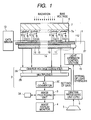
- FIG. 1 is a block diagram showing the configuration of an image pickup apparatus according to a first embodiment of the invention and the internal structure of a flat-panel radiation detector (radiation detector) of direct conversion type, of the image pickup apparatus.
- radiation detector radiation detector
- the radiological image pickup apparatus of the first embodiment includes a flat-panel radiation detector of direct conversion type (FPD) 1, an electric signal processing circuit 2, an image processing circuit 3, an image display monitor 4, an operation section 5, and a central processing unit 6, as shown in FIG. 1.
- the flat-panel radiation detector of direct conversion type (FPD) 1 detects and takes out the spatial distribution of incident radiation passing through the object whose image is to be picked up (not shown) as an electric signal.
- the electric signal processing circuit 2 amplifies the electric signal taken out from the FPD 1.
- the image processing circuit 3 creates a radiological image of the obj ect based on the electric signal amplified by the electric signal processing circuit 2.
- the image display monitor 4 displays the radiological image created by the image processing circuit 3.
- the operator performs entry operation required for picking up an image the through operation section 5.
- the central processing unit 6 performs necessary operations and control in response to entry operation performed through the operation section 5 and the advance state of the image pickup process.
- the radiological image pickup apparatus the radiological image corresponding to the radiological image passing through the object projected onto the FPD 1 as radiation is applied to the object is displayed on the image display monitor 4.
- a common electrode 8 for applying a bias voltage is formed on one side of a semiconductor layer 7 sensitive to radiation and a two-dimensional array made up of a large number of split electrodes 9 is formed on an opposite side.
- a transparent glass substrate (TFT substrate) 12 is disposed on the split electrode 9 formation side of the semiconductor layer 7.
- the transparent glass substrate 12 is formed with pairs of thin-film transistor switches (TFT switches) 10 and capacitors 11, each pair for each spilt electrode 9, provided in a one-to-one correspondence with pixels of a radiological image.
- a gate driver 13 switches on and off the TFT switches 10 in order according to an external scan signal for reading the charges accumulated in the capacitors 11, whereby an electric signal is taken out and the spatial distribution of the incident radiation is detected.
- an intermediate layer 7a is placed between the semiconductor layer 7 and the split electrodes 9.
- the electric signal processing circuit 2 amplifies the taken-out electric signal according to the gain value set by the central processing unit 6 (gain setup value) and can also increase or decrease the gain setup value.
- the gain setup value usually is set so that it is decreased if the assumed incident radiation strength increases and that it is increased if the assumed incident radiation strength decreases (namely, so that the incident radiation strength and the gain setup value are in inverse proportion).
- the electric signal processing circuit 2 is made up of a charge (electric current)-voltage converter 2A, a multiplexer 2B, and an A/D converter 2C, and the gain setup value is set in the charge-voltage converter 2A.
- the radiation strength of a radiation source (not shown) is also controlled by the central processing unit 6, and the central processing unit 6 sets the gain setup value of the electric signal processing circuit 2 matching the radiation strength of the radiation source.
- the radiation strength may be detected separately and the gain setup value matching the detected radiation strength may be set automatically by the central processing unit 6.
- the image processing circuit 3 has a correction coefficient registration section 3A for registering an offset correction coefficient and a sensitivity correction coefficient.
- the offset correction coefficient is used for correcting location variations in offset between electric signals caused by location nonuniformity of the detection channel of the FPD 1 for each electric signal to create a radiological image.
- the sensitivity correction coefficient is used for correcting location variations in sensitivity between electric signals caused by location nonuniformity of the detection channel of the FPD 1 for each electric signal to create a radiological image.
- the image processing circuit 3 performs variation correction processing in the offset and the sensitivity between the electric signals based on the previously registered offset correction coefficient and sensitivity correction coefficient.
- the image pickup apparatus of the embodiment includes a light application mechanism 14 and a light strength control section 15.
- the light applicationmechanism (light application section) 14 applies light to the entire surface of the split electrode 9 formation side of the semiconductor layer 7 sensitive to radiation.
- the light strength control section 15 controls the light application mechanism 14 so as to increase or decrease the strength of light applied by the light application mechanism 14 in response to a decrease or an increase in the gain setup value of the electric signal processing circuit 2.
- the light strength control section 15 controls the light application mechanism 14 so that the strength of light applied by the light application mechanism 14 increase if the gain setup value of the electric signal processing circuit 2 decreases and that the strength of light applied by the light application mechanism 14 decreases if the gain setup value increases (namely, so that the gain setup value and the light strength are in inverse proportion).
- the light strength control section 15 controls the light application mechanism 14 so that the strength of light applied by the light application mechanism 14 and the incident radiation strength are in direct proportion.
- proper applied light strength is previously experimentally calculated about each gain setup value and the applied light strength is registered in association with each gain setup value. Then, at setting the gain setup value, the corresponding applied light strength is read and is set in the light strength control section 15.
- a proper gain setup value and a proper applied light strength may be registered in association with each other for each radiation strength. Then, if the radiation strength is set, automatically the proper gain setup value and the proper applied light strength may be set.
- the light application mechanism 14 may include a light guide plate 16 made of a transparent acrylic resin disposed so as to overlap the back of the TFT substrate 12 and a light emission body 17 such as a light emitting diode or a cold-cathode tube placed on a side end face of the light guide plate 16, as shown in FIG. 1.
- the surface of the light guide plate 16 as the face overlapping the TFT substrate 12 may be micromachined (subj ected to surface roughness treatment) and a reflection sheet 18 may be attached to the back of the light guide plate 16.
- a dispersion sheet 19 may be placed between the TFT substrate 12 and the light guide plate 16.
- light of the light emission body 17 passes through the light guide plate 16 while it is reflected on the reflection sheet 18, and is applied through the micromachined surface of the light guide plate 16 and the dispersion sheet 19, so that the light can be applied efficiently and uniformly to the split electrode 9 formation side of the semiconductor layer 7.
- a surface light emitting diode may be put on the TFT substrate 12 with a transparent adhesive with its light emitting face directed for the TFT substrate 12.
- the light strength control section 15 controls the light emission amount of the light emission body 17 so that the light strength of the light emission body 17 increases or decreases in response to a decrease or an increase in the gain setup value, and also controls so as to enable the light application mechanism 14 to apply light not only during detection of radiation, but also before or after detection of radiation.
- the semiconductor layer 7 and the intermediate layer 7a will be discussed more specifically.
- the wavelength of light applied to the semiconductor layer 7 and the intermediate layer 7a is a wavelength shorter than the transmittance half wavelength of the semiconductor layer 7 and the intermediate layer 7a and longer than the wavelength corresponding to band gap energy.
- the wavelength of applied light is shorter than the transmittance half wavelength of the used semiconductor and is longer than the wavelength corresponding to band gap energy.
- the applied light enters a part of the semiconductor layer 7 deeply and a dead area widens.
- the energy of the applied light is smaller than the gap band energy, and thus damage to the semiconductor layer 7 (occurrence of crystalline defect) caused by the applied light and an increase in dark current caused by charge detection by the applied light itself do not occur.
- this mode is particularly effective because damage action to the semiconductor caused by the applied light is large in amorphous semiconductor such as amorphous selenium (a-Se).
- a-Se amorphous selenium
- the wavelength at which the transmittance for the intermediate layer 7a becomes 10% is about 710 nm, for example, when amorphous selenium (a-Se) is used for the intermediate layer 7a; it is about 660 nm when a thin film of antimonous sulfide (Sb 2 S 3 ) is used for the intermediate layer 7a.
- a-Se amorphous selenium
- SB 2 S 3 antimonous sulfide
- the semiconductor layer 7 is any of an amorphous substance of undoped Se or an undoped Se compound, an amorphous substance of Se doped with As or Te, or Se compound doped with As or Te, an amorphous substance of Se doped with alkali metal of Na, K, Li, etc., or an Se compound doped with alkali metal of Na, K, Li, etc., an amorphous substance of Se doped with halogen of F, Cl, etc., or an Se compound doped with halogen of F, Cl, etc., or an amorphous substance of Se doped with As, Te, alkali metal of Na, K, Li, etc., and halogen of F, Cl, etc., in combination or Se compound.
- the semiconductor layer 7 is a polycrystalline substance of any of compound semiconductors CdTe, CdZnTe, PbI 2 , HgI 2 , TlBr, or GaAs or a polycrystalline substance of the compound semiconductor doped with halogen of F, Cl, etc.
- the wavelength of light applied to the intermediate layer 7a is shorter than the transmittance half wavelength of the intermediate layer 7a; further preferably it is shorter than the wavelength at which the transmittance for the intermediate layer 7a becomes 10%. If the intermediate layer 7a has more defects than the semiconductor layer 7 and charges accumulate in the intermediate layer 7a more easily than the semiconductor layer 7, bend of an electric field occurs only in the intermediate layer 7a. Therefore, in this case, as light is applied to the intermediate layer 7a, fluctuations in sensitivity and occurrence of residual output caused by the effect of the charges accumulating in the space between the split electrodes 9 are eliminated.
- the wavelength of applied light is made shorter than the transmittance half wavelength of the intermediate layer 7a, most applied light is absorbed in the intermediate layer 7a, so that the applied light reaching the semiconductor layer 7 can be lessened. Therefore, dark current of the semiconductor layer 7 caused by the applied light can also be suppressed.
- the intermediate layer 7a is any of an amorphous substance of undoped Se or an undoped Se compound, an amorphous substance of Se doped with As or Te, or Se compound doped with As or Te, an amorphous substance of Se doped with alkali metal of Na, K, Li, etc., or an Se compound doped with alkali metal of Na, K, Li, etc., an amorphous substance of Se doped with halogen of F, Cl, etc., or an Se compound doped with halogen of F, Cl, etc., or an amorphous substance of Se doped with As, Te, alkali metal of Na, K, Li, etc., and halogen of F, Cl, etc., in combination or Se compound.
- the material of the semiconductor layer 7 and that of the intermediate layer 7a are made different.
- the intermediate layer 7a is a polycrystalline substance of any of compound semiconductors Sb 2 S 3 , CeO 2 , CdS, CdSe, CdTe, CdZnTe, ZnSe, ZnTe, ZnS, PbI 2 , HgI 2 , TlBr, or GaAs or a polycrystalline substance of the compound semiconductor doped with halogen of F, Cl, etc., or multilayer using the polycrystalline substances in combination.
- the filter effect can be provided for dealing with the case where it is necessary to apply light to both the semiconductor layer 7 and the intermediate layer 7a because charges accumulate in both the semiconductor layer 7 and the intermediate layer 7a.
- the intermediate layer 7a is made to have the transmission limit wavelength between the transmittance half wavelength of the semiconductor layer 7 and the wavelength corresponding to the band gap energy, whereby the filter effect is produced for applying light to any desired depth.
- the short wavelength component of wavelength components of white light is absorbed in the intermediate layer 7a and does not deeply reach the semiconductor layer 7 and most light can be made to act on the intermediate layer 7a without causing light application damage of the semiconductor layer 7 or an increase in dark current.
- the long wavelength component can be allowed to pass through the intermediate layer 7a to reach the semiconductor layer 7 and can be made to act thereon.
- the intermediate layer 7a mentioned here is a layer having carrier selectivity and has the effect of suppressing dark current, etc.
- the carrier selectivity refers to the property of remarkable difference between electrons and holes of charge transfer carriers in a semiconductor in the contribution rate to the charge transfer action.
- substances with large contribution of electrons to the charge transfer action includes polycrystalline substances such as CeO 2 , CdS, and CdSe of n-type semiconductors and amorphous substances of amorphous Se, etc., doped with alkali metal or As or Te for lowering contribution of holes.
- substances with large contribution of holes to the charge transfer action includes polycrystalline substances such as ZnSe, ZnTe, and ZnS of p-type semiconductors and amorphous substances of amorphous Se, etc., doped with halogen for lowering contribution of electrons.
- substances for providing large contribution of electrons or large contribution of holes depending on the film formation condition such as Sb 2 S 3 , CdTe, CdZnTe, PbI 2 , HgI 2 , TlBr, or undoped amorphous Se or Se compound.
- the transmittance half wavelength is 740 mm and the wavelength corresponding to the band gap energy 2.2 eV is 560 nm. Therefore, a material having a transmission limit wavelength in the range of 560 nm to 740 nm may be used to form the intermediate layer 7a.
- the transmission limit wavelength of a thin film of antimonous sulfide (Sb 2 S 3 ) 1 ⁇ m thick is 580 nm and thus if a thin film of antimonous sulfide 1 ⁇ m thick is formed as the intermediate layer 7a between amorphous selenium and the split electrodes 9, the short wavelength component of 580 nm or less, of applied white light is cut and the energy of the applied light becomes smaller than the band gap energy. Therefore, damage to the semiconductor layer 7 caused by the applied light and an increase in dark current are eliminated.
- the material and thickness of the intermediate layer 7a need to be selected according to the material of the semiconductor layer 7 to be used, the need for limiting the wavelength of the applied light is eliminated and the configuration involved in light application can be simplified. In other words, even if a white light source is used rather than a single-color light source as the applied light source, a radiation detector with no fluctuations in sensitivity can also be provided without causing light application damage or an increase in dark current.
- the intermediate layer 7a may be placed just below the common electrode 8 rather than placed just above the split electrodes 9 as described above and further if the intermediate layer 7a is placed both just above the split electrodes 9 and just below the common electrode 8, a similar advantage to that of the configuration described above can also be provided. At the time, the materials of the intermediate layers 7a need not be the same.
- the light strength control section 15 controls the light application mechanism 14, the applied light strength increases or decreases in response to a decrease or an increase in the gain setup value of the electric signal processing circuit 2, as described above.
- light application of the light application mechanism 14 carries an increase in electric signal with a dark current component added to the electric signal.
- the dark current component accompanying light application of the light application mechanism 14 increases or decreases in response to an increase or a decrease in the applied light strength; the dark current component increases as the applied light strength increases.
- the dynamic range of the electric signal processing circuit 2 is narrowed as much as the amplifieddark current component occupies the output range of the electric signal processing circuit 2; if the gain setup value increases, the amplification degree of the dark current component increases and therefore for the same amount of the dark current component, if the gain setup value increases, the degree of narrowing the dynamic range also increases.
- the gain setup value of the electric signal processing circuit 2 increases, the strength of light applied by the light application mechanism 14 is decreased and the dark current component decreases and thus the increase in the gain setup value is offset by the decrease in the dark current component and narrowing the dynamic range with the increase in the gain setup value is suppressed.
- the gain setup value of the electric signal processing circuit 2 decreases, the strength of light applied by the light application mechanism 14 is increased and the dark current component increases. Then, the increase in the dark current component is offset by the decrease in the gain setup value and narrowing the dynamic range with the increase in the applied light strength is suppressed.
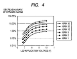
- FIG. 2 is a graph showing change in the illuminance (light strength) of the light emitting diode (LED) of the light emission body 17 of the light application mechanism 14 in response to change in the application voltage of the LED and change in the dark current component produced by light application of the LED (dark current increment of the FPD 1).
- FIG. 2 assumes that the gain setup value of the electric signal processing circuit 2 is 30 and the dynamic range is 8000 LSB. When the gain setup value is changed, the dark current component produced by light application of the LED becomes [GA/30] times if the gain setup value is GA.
- the optimum application voltage to the LED is calculated in accordance with how much the actual dark current component produced by light application of the LED occupies the dynamic range (decreasing rate of dynamic range).
- FIG. 3 is a list of numeric data indicating the application voltages of the LED and the decreasing rates of the dynamic range corresponding thereto for each representative gain setup value.
- FIG. 4 is a graph to indicate the correspondence between the application voltage of the LED and the decreasing rate of the dynamic range for each representative gain setup value.
- the decreasing rate of the dynamic range as a guideline varies depending on the type of radiological image of object to be picked up, etc.; for a medical radiological image requiring a wide dynamic range, it is desirable that the decreasing rate of the dynamic range should be 1% or less. Therefore, if the optimum application voltages of the LED for stepwise gain setup values in the electric signal processing circuit 2 are calculated, they are as listed in Table 1. Gain 1 2 5 10 20 30 Optimum LED voltage [V] 10 8.5 7.7 7.3 7.2 7.0
- the specific control systems of the light strength of the light emission body 17 of the light application mechanism 14 are as follows:
- the split electrodes 9 are transparent or semitransparent at the wavelength of the light applied by the light application mechanism 14. If the split electrodes 9 are thus transparent or semitransparent, the applied light is applied not only to the space between the split electrodes 9, but also to the split electrode 9 formation area. Thus, if radiation at a higher rate than the taking-out speed of charges is incident and charges once accumulate in the proximity of the split electrodes 9, they are instantly again excited by the energy of the applied light and Kinetic energy is given, so that the potential profile is not distorted and the potential in the proximity of the split electrodes 9 does not rise. Therefore, for example, to use a-Se which needs to be used with a high bias applied, the normal operation of the TFT switches 10 can also be maintained.
- the strength of the light applied by the light application mechanism 14 is reflected.
- the offset correction coefficient and the sensitivity correction coefficient are previously calculated by the image processing circuit 3 or the central processing unit 6 using a phantom (standard object) for registering the correction coefficients and are registered in the correction coefficient registration section 3A.
- the strength of the light appliedby the light application mechanism 14 is previously assumed to be in several steps and the offset correction coefficient and the sensitivity correction coefficient are calculated in each assumed step of the light strength and are registered in the correction coefficient registration section 3A.
- the offset correction coefficient and the sensitivity correction coefficient corresponding to the strength of the light applied in actual picking up an image are read and variation correction processing is performed.
- the image processing circuit 3 performs offset and sensitivity variation correction processing so that the strength of the light appliedbythe light application mechanism 14 is reflected based on the offset correction coefficient and the sensitivity correction coefficient already registered in the correction coefficient registration section 3A. Consequently, an error can be prevented from occurring in the offset and sensitivity variation corrections as light is applied by the light application mechanism 14.
- the forming method of the image pickup apparatus of the first embodiment is as follows:
- transparent electrodes of ITO films, etc. are formed on the TFT substrate 12 as the split electrodes 9 and then a thin film of antimonous sulfide (Sb 2 S 3 ) 1 ⁇ m thick is first formed as the intermediate layer 7a and next a thick film of amorphous selenium (a-Se) semiconductor 1 mm thick is formed as the semiconductor layer 7 sensitive to radiation. Then, a thin film of gold (Au) 0.1 ⁇ m thick is formed on the thick film of amorphous selenium (a-Se) semiconductor as the common electrode 8.
- a surface light emitting diode of green light emitting type is put on the back of the TFT substrate 12 with a transparent adhesive, whereby the light application mechanism 14 is disposed.
- the radiation detection operation of the image pickup apparatus of the embodiment is as follows:
- X-rays applied under the condition of tube voltage 55 kV and tube current 80 mA from an X-ray tube with an AL filter placed at a distance of 1 m from the FPD 1 were used.
- an AL filter 1 mm thick was used;
- an AL filter 26 mm thick was used.
- the digital output of the electric signal processing circuit 2 was set to the full range of 8000 [LSB].
- the response output waveforms of the electric signal processing circuit 2 when X-rays were applied for four seconds and then stopped in operation conditions (1) to (5) listedbelow were measured, and the decreasing rate of the dynamic range caused by the dark current increment produced by light application, the degree of fluctuations in the detection sensitivity, and the degree of occurrence of residual output were calculated from the measurement data.
- FIGS. 5 and 6 show the measurement results of the response output waveforms of the electric signal processing circuit 2, and Table 2 lists the results of the decreasing rate of the dynamic range, the degree of fluctuations in the detection sensitivity, the degree of occurrence of residual output, and the like.
- the operation conditions (1) and (2) are applied to the first embodiment, and the operation conditions (3) to (5) are applied to comparative examples. Fluctuations in detection sensitivity Occurrence of residual output Dark current increment Decreasing rate of dynamic range Operation condition (1) Small Small 65 LSB 0.81% Operation condition (2) Small Small 60 LSB 0.75% Operation condition (3) Medium Medium 2 LSB 0.03% Operation condition (4) Small Small 1950 LSB 24% Operation condition (5) Large Large None 0%
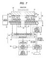
- FIG. 7 is a block diagram showing the configuration of an image pickup apparatus according to a second embodiment of the invention and the internal structure of a flat-panel radiation detector (radiation detector) of indirect conversion type, of the image pickup apparatus.
- the image pickup apparatus of the second embodiment has the same configuration and advantages as the image pickup apparatus of the first embodiment except that it detects radiation using a flat-panel radiation detector (radiation detector) of indirect conversion type and therefore parts identical with or similar to those previously described with reference to FIG. 1 are denoted by the same reference numerals in FIG. 7 and will not be discussed again.
- a flat-panel radiation detector radiation detector
- the radiological image pickup apparatus of the second embodiment includes a flat-panel radiation detector of indirect conversion type (FPD) 20, an electric signal processing circuit 2, an image processing circuit 3, an image display monitor 4, an operation section 5, and a central processing unit 6, as shown in FIG. 7.
- the flat-panel radiation detector of indirect conversion type (FPD) 20 detects and takes out the spatial distribution of incident radiation passing through the object whose image is to be picked up (not shown) in the form of an electric signal.
- the electric signal processing circuit 2 amplifies the electric signal taken out from the FPD 20.
- the image processing circuit 3 creates a radiological image of the object based on the electric signal amplified by the electric signal processing circuit 2.
- the image display monitor 4 displays the radiological image created by the image processing circuit 3.
- the operator performs entry operation required for picking up an image through the operation section 5.
- the central processing unit 6 performs necessary operations and control in response to entry operation performed through the operation section 5 and the advance state of the image pickup process. Therefore, the radiological image corresponding to the radiological image passing through the object projected onto the FPD 20 as radiation is applied to the object is displayed on the image display monitor 4.
- a two-dimensional array made up of a large number of semiconductor optical sensors 24 is formed on one side of a radiation-light conversion layer 21 for converting radiation into light.
- the semiconductor optical sensors 24 are provided by electrically splitting a semiconductor layer 22 sensitive to light, each having an electric signal output electrode 23 on the back of the semiconductor layer 22.
- a transparent glass substrate (TFT substrate) 27 is disposed on the semiconductor optical sensor 24 formation side of the radiation-light conversion layer 21.
- the transparent glass substrate (TFT substrate) 27 is formed with pairs of thin-film transistor switches (TFT) 25 and capacitors 26, each pair for each semiconductor optical sensor 24, provided in a one-to-one correspondence with pixels of a radiological image.
- a gate driver 28 switches on and off the TFT switches 25 in order according to an external scan signal for reading the charges accumulated in the capacitors 26, whereby light occurring in the radiation-light conversion layer 21 by the incident radiation is taken out as an electric signal from each of the semiconductor optical sensors 24 and the spatial distribution of the incident radiation is detected.
- the image pickup apparatus of the second embodiment also includes a light application mechanism (light application section) 29 and a light strength control section 30.
- the light application mechanism 29 applies light to the entire surface of the semiconductor optical sensor 24 formation side of the radiation-light conversion layer 21.
- the light strength control section 30 controls the light application mechanism 29 so as to increase or decrease the strength of light applied by the light application mechanism 29 in response to a decrease or an increase in the gain setup value of the electric signal processing circuit 2.
- the light strength control section 30 controls the light application mechanism 29 so that the strength of light applied by the light application mechanism 29 increases if the gain setup value of the electric signal processing circuit 2 decreases and that the strength of light applied by the light application mechanism 29 decreases if the gain setup value increases (namely, so that the gain setup value and the light strength are in inverse proportion).
- the light strength control section 30 controls the light application mechanism 29 so that the strength of light applied by the light application mechanism 29 and the incident radiation strength are in direct proportion.
- proper applied light strength is previously experimentally calculated about each gain setup value and the applied light strength is registered in association with each gain setup value and to set the gain setup value, the corresponding applied light strength is read and is set in the light strength control section 30.
- a proper gain setup value and a proper applied light strength maybe registered in association with each other for each radiation strength and if the radiation strength is set, automatically the proper gain setup value and the proper applied light strength may be set.
- the electric signal output electrode 23 of each the semiconductor optical sensor 24 on the side thereof on which light from the light application mechanism 29 is incident is formed of an opaque material such as Al or Ta and has a light shield function for shielding the light from the light application mechanism 29 so that the light is not directly detected by the semiconductor optical sensor 24.
- the light from the light application mechanism 29 is not radiation to be detected and thus is not directly detected by the semiconductor optical sensor 24.
- the light application mechanism 29 may include a light guide plate 31 made of a transparent acrylic resin disposed so as to overlap the back of the TFT substrate 27 and a light emission body 32 such as a light emitting diode or a cold-cathode tube placed on a side end face of the light guide plate 31, as shown in FIG. 7.
- the surface of the light guide plate 31 as the face overlapping the TFT substrate 27 may be micromachined (subjected to surface roughness treatment) and a reflection sheet 33 may be attached to the back of the light guide plate 31.
- a dispersion sheet 34 maybe placed between the TFT substrate 27 and the light guide plate 31.
- light of the light emission body 32 passes through the light guide plate 31 while it is reflected on the reflection sheet 33, and is applied through the micromachined surface of the light guide plate 31 and the dispersion sheet 34, so that the light can be applied efficiently and uniformly to the semiconductor optical sensor 24 formation side of the radiation-light conversion layer 21.
- a surface light emitting diode may be put on the TFT substrate 27 with a transparent adhesive with its light emitting face directed for the TFT substrate 27.
- the light strength control section 30 controls the light emission amount of the light emission body 32 so that the light strength of the light emission body 32 increases or decreases in response to a decrease or an increase in the gain setup value, and also controls so as to enable the light application mechanism 29 to apply light not only during detection of radiation, but also before or after detection of radiation.
- the light application mechanism 29 applies light to the semiconductor optical sensor 24 formation side of the radiation-light conversion layer 21 for converting radiation into light in the FPD 20
- space charges produced by the light application accumulate in the space between the semiconductor optical sensors 24 and thus the charges occurring as radiation is incident do not accumulate and are taken out. Consequently, change in the effective sensitive area does not occur and fluctuations in the detection sensitivity of the FPD 20 can be circumvented.
- the light strength control section 30 controls the light application mechanism 29, the applied light strength increases or decreases in response to a decrease or an increase in the gain setup value of the electric signal processing circuit 2, as described above.
- light application of the light application mechanism 29 carries an increase in electric signal with a dark current component added to the electric signal.
- the dark current component accompanying light application of the light application mechanism 29 increases or decreases in response to an increase or a decrease in the applied light strength; the dark current component increases as the applied light strength increases.
- the dynamic range of the electric signal processing circuit 2 is narrowed as much as the amplified dark current component occupies the output range of the electric signal processing circuit 2; if the gain setup value increases, the amplification degree of the dark current component increases and therefore for the same amount of the dark current component, if the gain setup value increases, the degree of narrowing the dynamic range also increases.
- the gain setup value of the electric signal processing circuit 2 increases, the strength of light applied by the light application mechanism 29 is decreased and the dark current component decreases and thus the increase in the gain setup value is offset by the decrease in the dark current component and narrowing the dynamic range with the increase in the gain setup value is suppressed.
- the gain setup value of the electric signal processing circuit 2 decreases, the strength of light applied by the light application mechanism 29 is increased and the dark current component increases. Then, the increase in the dark current component is offset by the decrease in the gain setup value and narrowing the dynamic range with the increase in the applied light strength is suppressed.
- the light application section applies light to the split electrode formation side of the semiconductor layer sensitive to radiation in the radiation detector and space charges produced by the light application accumulate in the space between the split electrodes and thus the charges occurring as radiation is incident do not accumulate and are taken out. Consequently, change in the effective sensitive area does not occur and fluctuations in the detection sensitivity of the radiation detector canbe circumvented. If light application is continued still after incidence of radiation stops, the space charges accumulating in the space between the split electrodes are not taken out and continue to accumulate and therefore occurrence of residual output can also be circumvented.
- the gain setup value of the electric signal processing circuit increases, the strength of light applied by the light application section is decreased and the dark current component decreases and thus the increase in the gain setup value is offset by the decrease in the dark current component and narrowing the dynamic range with the increase in the gain setup value is suppressed.
- the gain setup value of the electric signal processing circuit decreases, the strength of light applied by the light application section is increased and the dark current component increases. Then, the increase in the dark current component is offset by the decrease in the gain setup value, narrowing the dynamic range with the increase in the applied light strength is also suppressed, and the dark current component narrowing the dynamic range does not widely occupy the output range of the electric signal processing circuit. Consequently, a situation in which the dynamic range is largely narrowed does not occur.
- the light application section applies light to the semiconductor optical sensor formation side of the radiation-light conversion layer in the radiation detector so that the light is not directly detected by the semiconductor optical sensors, and the light of the light application section is not directly detected by the semiconductor optical sensors, so that the detection operation of the semiconductor optical sensors is not hindered.
- Space charges produced by the light application accumulate in the space between the semiconductor optical sensors and thus the charges occurring as radiation is incident do not accumulate and are taken out. Consequently, change in the effective sensitive area does not occur and fluctuations in the detection sensitivity of the radiation detector can be circumvented.
- the gain setup value of the electric signal processing circuit increases, the strength of light applied by the light application section is decreased and the dark current component decreases and thus the increase in the gain setup value is offset by the decrease in the dark current component and narrowing the dynamic range with the increase in the gain setup value is suppressed.
- the gain setup value of the electric signal processing circuit decreases, the strength of light applied by the light application section is increased and the dark current component increases. Then, the increase in the dark current component is offset by the decrease in the gain setup value, narrowing the dynamic range with the increase in the applied light strength is also suppressed, and the dark current component narrowing the dynamic range does not widely occupy the output range of the electric signal processing circuit. Consequently, a situation in which the dynamic range is largely narrowed does not occur.
Landscapes
- Spectroscopy & Molecular Physics (AREA)
- Physics & Mathematics (AREA)
- Life Sciences & Earth Sciences (AREA)
- General Physics & Mathematics (AREA)
- High Energy & Nuclear Physics (AREA)
- Molecular Biology (AREA)
- Health & Medical Sciences (AREA)
- Food Science & Technology (AREA)
- Engineering & Computer Science (AREA)
- Measurement Of Radiation (AREA)
- Solid State Image Pick-Up Elements (AREA)
- Transforming Light Signals Into Electric Signals (AREA)
- Light Receiving Elements (AREA)
- Apparatus For Radiation Diagnosis (AREA)
Applications Claiming Priority (2)
| Application Number | Priority Date | Filing Date | Title |
|---|---|---|---|
| JP2003073738A JP3757946B2 (ja) | 2003-03-18 | 2003-03-18 | 放射線撮像装置 |
| JP2003073738 | 2003-03-18 |
Publications (1)
| Publication Number | Publication Date |
|---|---|
| EP1467227A2 true EP1467227A2 (de) | 2004-10-13 |
Family
ID=32866680
Family Applications (1)
| Application Number | Title | Priority Date | Filing Date |
|---|---|---|---|
| EP04004741A Withdrawn EP1467227A2 (de) | 2003-03-18 | 2004-03-01 | Gerät zur Aufnahme von Röntgenbildern |
Country Status (6)
| Country | Link |
|---|---|
| US (1) | US7038214B2 (de) |
| EP (1) | EP1467227A2 (de) |
| JP (1) | JP3757946B2 (de) |
| KR (1) | KR100585877B1 (de) |
| CN (1) | CN1281973C (de) |
| CA (1) | CA2459268C (de) |
Cited By (3)
| Publication number | Priority date | Publication date | Assignee | Title |
|---|---|---|---|---|
| EP1798574A1 (de) * | 2005-11-16 | 2007-06-20 | Hitachi, Ltd. | Nuklearmedizinisches Abbildungssystem und Verfahren |
| US7952058B2 (en) | 2005-12-20 | 2011-05-31 | Canon Kabushiki Kaisha | Radiation detection apparatus and radiation detection system having a light source located to reduce dark current |
| EP2023163A3 (de) * | 2007-07-31 | 2017-01-18 | FUJIFILM Corporation | Bilderkennungsvorrichtung |
Families Citing this family (20)
| Publication number | Priority date | Publication date | Assignee | Title |
|---|---|---|---|---|
| JP4254602B2 (ja) * | 2004-04-19 | 2009-04-15 | 株式会社島津製作所 | 二次元放射線検出器 |
| JP4622670B2 (ja) * | 2005-05-17 | 2011-02-02 | 株式会社島津製作所 | 2次元放射線検出器 |
| JP2007129347A (ja) * | 2005-11-01 | 2007-05-24 | Fujifilm Corp | 放射線固体検出器の残留電荷消去方法、および放射線画像記録読取装置 |
| JP4911966B2 (ja) * | 2005-12-12 | 2012-04-04 | キヤノン株式会社 | 放射線検出装置および放射線撮像システム |
| JP4989197B2 (ja) * | 2005-12-13 | 2012-08-01 | キヤノン株式会社 | 放射線撮像装置、放射線撮像システム、及び補正方法 |
| JP5300216B2 (ja) * | 2006-08-29 | 2013-09-25 | キヤノン株式会社 | 電子カセッテ型放射線検出装置 |
| JP5049739B2 (ja) * | 2006-11-01 | 2012-10-17 | キヤノン株式会社 | 放射線撮像装置 |
| JP5455312B2 (ja) * | 2007-03-13 | 2014-03-26 | キヤノン株式会社 | 放射線撮像装置、その制御方法、及びプログラム |
| JP5007632B2 (ja) * | 2007-09-04 | 2012-08-22 | 株式会社島津製作所 | 放射線撮像装置 |
| JP4793397B2 (ja) * | 2008-03-14 | 2011-10-12 | コニカミノルタエムジー株式会社 | 放射線画像検出器 |
| DE102008025199B3 (de) * | 2008-05-27 | 2009-09-17 | Siemens Aktiengesellschaft | Strahlungsdetektor und Herstellungsverfahren sowie Strahlungserfassungseinrichtung |
| JP5377081B2 (ja) * | 2009-06-01 | 2013-12-25 | キヤノン株式会社 | 放射線撮影装置及びその制御方法 |
| WO2010150381A1 (ja) * | 2009-06-25 | 2010-12-29 | キヤノン株式会社 | 放射線撮像装置及び放射線撮像システム、それらの制御方法及びそのプログラム |
| CA2829094A1 (en) | 2011-03-07 | 2012-11-29 | Loma Linda University Medical Center | Systems, devices and methods related to calibration of a proton computed tomography scanner |
| JP5895650B2 (ja) * | 2012-03-28 | 2016-03-30 | ソニー株式会社 | 撮像装置および撮像表示システム |
| CN103424768A (zh) * | 2012-05-25 | 2013-12-04 | 同方威视技术股份有限公司 | 一种用于探测器系统的增益稳定装置及其控制方法 |
| CN103995010B (zh) * | 2014-01-26 | 2016-03-23 | 浙江康源医疗器械有限公司 | X-射线成像空间分布不均匀性的校正方法 |
| JP6442154B2 (ja) | 2014-04-23 | 2018-12-19 | 浜松ホトニクス株式会社 | 画像取得装置及び画像取得方法 |
| WO2020073626A1 (en) * | 2018-10-09 | 2020-04-16 | Shenzhen GOODIX Technology Co., Ltd. | Image sensor with dynamic charge-domain sampling |
| KR102447358B1 (ko) * | 2020-12-01 | 2022-09-26 | (주)아이스트 | X선 라인 검출기 영상 보정 시스템 및 이를 이용한 영상 보정 방법 |
Family Cites Families (3)
| Publication number | Priority date | Publication date | Assignee | Title |
|---|---|---|---|---|
| US5886353A (en) * | 1995-04-21 | 1999-03-23 | Thermotrex Corporation | Imaging device |
| JP4156120B2 (ja) * | 1999-02-17 | 2008-09-24 | 富士フイルム株式会社 | 放射線画像撮影方法および装置 |
| JP4211435B2 (ja) * | 2002-08-30 | 2009-01-21 | 株式会社島津製作所 | 放射線検出器 |
-
2003
- 2003-03-18 JP JP2003073738A patent/JP3757946B2/ja not_active Expired - Fee Related
-
2004
- 2004-02-27 KR KR1020040013503A patent/KR100585877B1/ko not_active Expired - Fee Related
- 2004-03-01 EP EP04004741A patent/EP1467227A2/de not_active Withdrawn
- 2004-03-01 CA CA002459268A patent/CA2459268C/en not_active Expired - Fee Related
- 2004-03-01 CN CNB2004100283312A patent/CN1281973C/zh not_active Expired - Fee Related
- 2004-03-01 US US10/790,397 patent/US7038214B2/en not_active Expired - Fee Related
Cited By (3)
| Publication number | Priority date | Publication date | Assignee | Title |
|---|---|---|---|---|
| EP1798574A1 (de) * | 2005-11-16 | 2007-06-20 | Hitachi, Ltd. | Nuklearmedizinisches Abbildungssystem und Verfahren |
| US7952058B2 (en) | 2005-12-20 | 2011-05-31 | Canon Kabushiki Kaisha | Radiation detection apparatus and radiation detection system having a light source located to reduce dark current |
| EP2023163A3 (de) * | 2007-07-31 | 2017-01-18 | FUJIFILM Corporation | Bilderkennungsvorrichtung |
Also Published As
| Publication number | Publication date |
|---|---|
| CA2459268A1 (en) | 2004-09-18 |
| JP3757946B2 (ja) | 2006-03-22 |
| KR20040082279A (ko) | 2004-09-24 |
| CN1530074A (zh) | 2004-09-22 |
| US7038214B2 (en) | 2006-05-02 |
| US20040183025A1 (en) | 2004-09-23 |
| CA2459268C (en) | 2007-11-20 |
| CN1281973C (zh) | 2006-10-25 |
| JP2004281882A (ja) | 2004-10-07 |
| KR100585877B1 (ko) | 2006-06-01 |
Similar Documents
| Publication | Publication Date | Title |
|---|---|---|
| US7038214B2 (en) | Radiological image pickup apparatus | |
| US8981304B2 (en) | Radiation detector | |
| US7732776B2 (en) | Radiation imaging apparatus, drive method and program of the radiation imaging apparatus | |
| US6995375B2 (en) | Split-electrode radiation detector free of sensibility variations and after-outputs | |
| US7897930B2 (en) | Radiation imaging apparatus and radiation imaging system | |
| US8680472B2 (en) | Radiation detecting apparatus and radiation imaging system | |
| US11487027B2 (en) | Radiation imaging apparatus and radiation imaging system | |
| EP0792066B1 (de) | Photoelektrische Umwandlungsvorrichtung und Ansteuermethode dafür | |
| CN101523898B (zh) | 放射线成像装置和放射线成像系统 | |
| US6791091B2 (en) | Wide dynamic range digital imaging system and method | |
| CN109521455B (zh) | 一种实现自动增益切换的x射线影像探测器及其方法 | |
| US9910172B2 (en) | Temperature compensation for thin film transistors in digital X-ray detectors | |
| EP2023163A2 (de) | Bilderkennungsvorrichtung | |
| US20030043959A1 (en) | X-ray detector provided with a heating device | |
| US7541595B2 (en) | Electromagnetic radiation detecting apparatus, radiation detecting apparatus, radiation detecting system and laser processing method | |
| JP5464064B2 (ja) | 可搬型放射線画像撮影装置および放射線画像撮影システム | |
| EP3410159B1 (de) | Lichtdetektionsvorrichtung und betriebsverfahren dafür | |
| EP2757389A2 (de) | Hochauflösende Bildgebung mit Röntgenstrahlen mit dünnen, flexiblen digitalen Sensoren | |
| RU197875U1 (ru) | Детектор рентгеновского излучения с составным сцинтиллятором | |
| KR20250097297A (ko) | 엑스선 디텍터 | |
| CN1881598A (zh) | 电磁辐射检测设备、辐射检测设备和系统及激光处理方法 | |
| JP2004228515A (ja) | 放射線検出装置 | |
| HK1002479B (en) | Photoelectric conversion apparatus and driving method thereof |
Legal Events
| Date | Code | Title | Description |
|---|---|---|---|
| PUAI | Public reference made under article 153(3) epc to a published international application that has entered the european phase |
Free format text: ORIGINAL CODE: 0009012 |
|
| AK | Designated contracting states |
Kind code of ref document: A2 Designated state(s): AT BE BG CH CY CZ DE DK EE ES FI FR GB GR HU IE IT LI LU MC NL PL PT RO SE SI SK TR |
|
| AX | Request for extension of the european patent |
Extension state: AL LT LV MK |
|
| STAA | Information on the status of an ep patent application or granted ep patent |
Free format text: STATUS: THE APPLICATION HAS BEEN WITHDRAWN |
|
| 18W | Application withdrawn |
Effective date: 20120112 |