EP1467279A1 - Appareil d'exploitation et systeme d'exploitation - Google Patents
Appareil d'exploitation et systeme d'exploitation Download PDFInfo
- Publication number
- EP1467279A1 EP1467279A1 EP02760770A EP02760770A EP1467279A1 EP 1467279 A1 EP1467279 A1 EP 1467279A1 EP 02760770 A EP02760770 A EP 02760770A EP 02760770 A EP02760770 A EP 02760770A EP 1467279 A1 EP1467279 A1 EP 1467279A1
- Authority
- EP
- European Patent Office
- Prior art keywords
- arithmetic
- selecting information
- bus
- data
- processing device
- Prior art date
- Legal status (The legal status is an assumption and is not a legal conclusion. Google has not performed a legal analysis and makes no representation as to the accuracy of the status listed.)
- Withdrawn
Links
Images





Classifications
-
- G—PHYSICS
- G06—COMPUTING OR CALCULATING; COUNTING
- G06F—ELECTRIC DIGITAL DATA PROCESSING
- G06F9/00—Arrangements for program control, e.g. control units
- G06F9/06—Arrangements for program control, e.g. control units using stored programs, i.e. using an internal store of processing equipment to receive or retain programs
- G06F9/30—Arrangements for executing machine instructions, e.g. instruction decode
- G06F9/30098—Register arrangements
-
- G—PHYSICS
- G06—COMPUTING OR CALCULATING; COUNTING
- G06F—ELECTRIC DIGITAL DATA PROCESSING
- G06F9/00—Arrangements for program control, e.g. control units
- G06F9/06—Arrangements for program control, e.g. control units using stored programs, i.e. using an internal store of processing equipment to receive or retain programs
- G06F9/30—Arrangements for executing machine instructions, e.g. instruction decode
- G06F9/30003—Arrangements for executing specific machine instructions
- G06F9/30007—Arrangements for executing specific machine instructions to perform operations on data operands
- G06F9/3001—Arithmetic instructions
Definitions
- the invention relates to a processing device and processing system.
- the invention in particular, relates to a processing device and processing system that perform a series of operations on an input to produce an output.
- CPU Central Processing Unit
- DSP Digital Signal Processor
- ALU Arimetic Logic Unit
- the processing is high-speed if data flows through the arithmetic cells in order by the reserved operation program.
- ALU Arimetic Logic Unit
- the invention is based on the above points, so the objective is to provide a processing device and processing system that can perform high-speed and flexible processing.
- the invention includes multiple arithmetic cells each selecting a predetermined one of multiple inputs, performing a reserved operation, and producing an output.
- the output of each arithmetic cell is supplied to one of the inputs of multiple arithmetic cells.
- the processing is distributed in advance among the multiple arithmetic cells and data flows in a preset order, so the series of operations can be performed in pipelining and the processing is high-speed.
- Fig.1 is the block diagram of an implementation example of the invention.
- Data processing system 1 of the implementation example involves data processing module 11, input device 12 and display 13.
- Data processing module 11 involves CPU 21, wafer group 22 and 23, memory module 24, video wafer 25, PCI bus 26, PCI slot 27, hard disk drive 28, ROM 29, ISA bus 30, ISA slot 31 and USB port 32.
- CPU 21 receives data from wafer group 22, performs operations, and transmits the operation results back to wafer group 22.
- Wafer group 22 exchanges data with memory module 24 and video memory module 25 and, at the same time, exchanges data with PCI bus 26.
- Memory module 24 is composed of DRAM group, acting as temporary storage for CPU21.
- Video wafer 25 receives data from wafer group 22 and transmits to display 13. Display 13 displays the data from video wafer 25.
- PCI bus 26 connects with PCI slot 27.
- the PCI board which processing device 100 is mounted on is plugged in PCI slot 27.
- PCI bus 26 connects with wafer group 23.
- Wafer group 23 is the interface of PCI bus 26, hard disk drive 28, ROM 29, ISA bus 30 and USB port 32.
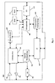
- Fig.2 is the block diagram of processing device 100.
- Processing device 100 is a printed circuit board 120 which input amplifier 101, output amplifier 102, I/O port 103, arithmetic unit 104, memory module 105, reserved working storage 106, I/F 107, microprocessor 108, communication working storage 109, ROM 110, RAM111 and microprocessor I/O port 112 are mounted on.
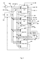
- Fig.3 is the block diagram of arithmetic unit 104.
- Arithmetic unit 104 involves N arithmetic cells 201-1 ⁇ 201-N (N is an integer not smaller than 2), bus 202-1 ⁇ 202-(N+3) and I/O units 203 and 204.
- Bus 202-1 receives output data of arithmetic cell 201-1; bus 202-2 receives output data of arithmetic cell 201-2.
- bus 202-3 ⁇ 202-(N-1) receives output data of arithmetic cells 201-3 ⁇ 202-(N-1) respectively, and bus 202-N receives output data of arithmetic cell 201-N.
- bus 202-(N+1) receives output data of input amplifier 101
- bus 202-(N+2) receives output data of I/O port 103
- bus 202-(N+3) receives output data of memory module 105.
- bus 202-1 ⁇ 202-(N+3) supply the input data of arithmetic cells 201-1 ⁇ 202-N and output units 203 and 204.
- Arithmetic cells 201-1 ⁇ 202-N receives the data on the preset buses among bus 202-1 ⁇ 202-(N+3), and performs the reserved operation.
- output unit 203 transmits the data on the preset bus among bus 202-1 ⁇ 202-(N+3) to memory module 105.
- Output unit 204 transmits the data on the preset bus among bus 202-1 ⁇ 202-(N+3) to I/O port 103.
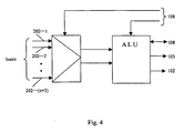
- Fig.4 is the block diagram of arithmetic cell 201-1.
- Arithmetic cell 201-1 consists of multiplexer 301 and arithmetic circuit 302.
- Bus 202-1 ⁇ 202-(N+3) are connected with inputs of multiplexer 301.
- Multiplexer 301 selects one or two buses among bus 202-1 ⁇ 202-(N+3) according to the bus-selecting information in reserved working storage 106, and transmits the data on the selected buses to arithmetic circuit 302.
- the input data to arithmetic circuit 302 is the data on the one or two buses selected by multiplexer 301.
- Arithmetic circuit 302 is mainly composed of ALU (Arithmetic Logic Unit), and performs the reserved operation on the data from multiplexer 301 according to operation-selecting information in reserved working storage 106.
- the operation result by arithmetic circuit 302 is transmitted to bus 202-1.
- arithmetic cells 201-2 ⁇ 201-N have the same architecture as arithmetic cells 201-1, so the illustrations of them are omitted.
- Fig.5 is the operation diagram of arithmetic circuit 302.
- Arithmetic circuit 302 is supplied the operation-selecting information C1 ⁇ C20 stored in advance in reserved working storage 106. Arithmetic circuit 302 performs the reserved operation according to operation-selecting information C1 ⁇ C20 in reserved working storage 106.
- arithmetic circuit 302 When the operation-selecting information in reserved working storage 106 is C1, arithmetic circuit 302 performs ADD/SUB operation on the data on the two buses selected by multiplexer 301. When the operation-selecting information in reserved working storage 106 is C2, arithmetic circuit 302 performs MULT operation on the data on the two buses selected by multiplexer 301.
- arithmetic circuit 302 When the operation-selecting information in reserved working storage 106 is C3, arithmetic circuit 302 performs DIV operation on the data on the two buses selected by multiplexer 301. When the operation-selecting information in reserved working storage 106 is C4, arithmetic circuit 302 performs AND logic operation on each bit of the data on the two buses selected by multiplexer 301.
- arithmetic circuit 302 When the operation-selecting information in reserved working storage 106 is C5, arithmetic circuit 302 performs OR logic operation on each bit of the data on the two buses selected by multiplexer 301. When the operation-selecting information in reserved working storage 106 is C6, arithmetic circuit 302 performs XOR logic operation on each bit of the data on the two buses selected by multiplexer 301.
- arithmetic circuit 302 When the operation-selecting information in reserved working storage 106 is C7, arithmetic circuit 302 performs INV logic operation on each bit of the data on the bus selected by multiplexer 301. When the operation-selecting information in reserved working storage 106 is C8, arithmetic circuit 302 performs shift logic operation with a predetermined number on the data on the bus selected by multiplexer 301.
- arithmetic circuit 302 delays the data on the bus selected by multiplexer 301.
- arithmetic circuit 302 transmits the data, which is on the bus selected by multiplexer 301, to bus 202-1 or I/O control unit selectively.
- arithmetic circuit 302 converts the data, which is on the bus selected by multiplexer 301, to analog signal and, then transmits to analog signal output line Laout.
- Analog signal output line Laout connects with output amplifier 102, and output amplifier 102 is to amplify the analog signal on signal output line Laout to transmits.
- arithmetic circuit 302 converts the analog signal, which is on analog signal input line Lain selected by multiplexer 301, to digit data. The digit data is then transmitted to bus 202-1.
- arithmetic circuit 302 When the operation-selecting information in reserved working storage 106 is C 13, arithmetic circuit 302 performs digital filtering with the preset filter factors on the data on the bus selected by multiplexer 301, and then transmits. That is to say, arithmetic circuit 302 acts as the digital filter with the expected characteristics.
- arithmetic circuit 302 transmits the data on the bus selected by multiplexer 301 to port 1 of microprocessor.
- Microprocessor operates on the data by the reserved operation program, and then transmits back to arithmetic circuit 302. Arithmetic circuit 302 transmits the processed data by microprocessor to bus 202-1.
- arithmetic circuit 302 transmits the data on the bus selected by multiplexer 301 to port 2 of microprocessor.
- Microprocessor operates on the data by the reserved operation program, and then transmits back to arithmetic circuit 302.
- Arithmetic circuit 302 transmits the processed data by microprocessor to bus 202-1.
- arithmetic circuit 302 transmits the data on the bus selected by multiplexer 301 to port 3 of microprocessor.
- Microprocessor operates on the data by the reserved operation program, and then transmits back to arithmetic circuit 302.
- Arithmetic circuit 302 transmits the processed data by microprocessor to bus 202-1.
- arithmetic circuit 302 When the operation-selecting information in reserved working storage 106 is C 17, arithmetic circuit 302 performs digital filtering with the preset low-pass filter factors on the data on the bus selected by multiplexer 301. When the operation-selecting information in reserved working storage 106 is C18, arithmetic circuit 302 performs digital filtering with the preset low-pass filter factors on the data on the bus selected by multiplexer 301.
- arithmetic circuit 302 transmits the absolute value of the data on the bus selected by multiplexer 301.
- expected buses are selected according to the operation-selecting information C1 ⁇ C20 in reserved working storage 106, and expected operation is performed on the data on the selected buses.
- arithmetic cells 201-2 ⁇ 201-N have the same architecture as arithmetic cells 201-1, so the illustrations of them are omitted.
- Bus 202-1 ⁇ 202-(N+3) are connected with inputs of output unit 203.
- Fig.6 is the block diagram of output unit 203.
- the key part of output unit 203 is multiplexer 401.
- Bus 202-1 ⁇ 202-(N+3) are connected with inputs of multiplexer 401. Furthermore, the data on the bus selected by the bus-selecting information in reserved working storage 106 is transmitted to I/O port by multiplexer 401.
- output unit 204 has the same architecture as output unit 203.
- Output data of output unit 203 is transmitted to memory module, and memory module views the data as address to export the corresponding data stored in memory module.
- the data in memory module corresponding to its address is in advance stored in microprocessor.
- the output data of memory module is transmitted to bus 201-(N+3), and then is transmitted to inputs of arithmetic cells 201-1 ⁇ 201-N and output unit 203.
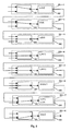
- Fig.7 and Fig.8 are the detailed operation diagrams of processing device.
- AM detecting which is realized by analog-to-digital conversion 501, band selecting 502, absolute value processing 503, clutter rejecting 504, envelope detecting 505, amplifying 506, quieting 507 and digital-to-analog conversion 508, is shown in Fig.7.
- Analog-to-digital conversion 501 is to convert the input analog signal to digital signal.
- Band selecting 502 is realized by digital filter to perform digital filtering on the digit data after analog-to-digital conversion 501.
- the output data of band selecting 502 is converted to absolute value for transmission by absolute value processing 503.
- the absolute value of the data is next processed by clutter rejecting 504.
- Clutter rejecting 504 is realized by digital low-pass filter to filter off the unnecessary signal components.
- Envelope detecting 505 is realized by digital low-pass filter to detect envelope from the output data of clutter rejecting 504.
- Amplifying 506 amplifies the digit data through multiplying digit data with a constant.
- Quieting 507 shuts off the digit data output as soon as quieting indication is active.
- Digital-to-analog conversion 508 converts the AM detecting digit data to analog signal.
- the above analog-to-digital conversion 501, band selecting 502, absolute value processing 503, clutter rejecting 504, envelope detecting 505, amplifying 506, quieting 507 and digital-to-analog conversion 508 can be performed by arithmetic cells 201-1 ⁇ 201-8 in order according to the bus-selecting information and operation-selecting information in reserved working storage 106.
- the bus-selecting information and operation-selecting information are set in reserved working storage 106.
- bus-selecting information and operation-selecting information in reserved working storage 106 are for arithmetic cells 201-1 ⁇ 201-N.
- bus-selecting information can be set just as multiplexer 301 of arithmetic cell 201-1 selects analog signal input line Lain.
- operation-selecting information C 12 can be set just as arithmetic circuit 302 performs analog-to-digital conversion.
- Bus-selecting information can be set just as multiplexer 301 of arithmetic cell 201-2 selects bus 202-1 which has received output of arithmetic cell 201-1.
- operation-selecting information C13 can be set just as arithmetic circuit 302 performs digital filtering.
- Bus-selecting information can be set just as multiplexer 301 of arithmetic cell 201-3 selects bus 202-2 which has received output of arithmetic cell 201-2.
- operation-selecting information C19 can be set just as arithmetic circuit 302 performs absolute value processing.
- Bus-selecting information can be set just as multiplexer 301 of arithmetic cell 201-4 selects bus 202-3 which has received output of arithmetic cell 201-3.
- operation-selecting information C17 can be set just as arithmetic circuit 302 performs low-pass filtering.
- Bus-selecting information can be set just as multiplexer 301 of arithmetic cell 201-5 selects bus 202-4 which has received output of arithmetic cell 201-4.
- operation-selecting information C18 can be set just as arithmetic circuit 302 performs low-pass filtering.
- Bus-selecting information can be set just as multiplexer 301 of arithmetic cell 201-6 selects bus 202-5 which has received output of arithmetic cell 201-5.
- operation-selecting information C2 can be set just as arithmetic circuit 302 performs multiplication operation.
- Bus-selecting information can be set just as multiplexer 301 of arithmetic cell 201-7 selects bus 202-6 which has received output of arithmetic cell 201-6.
- operation-selecting information C14 can be set just as arithmetic circuit 302 performs quieting operation with the help of microprocessor.
- Bus-selecting information can be set just as multiplexer 301 of arithmetic cell 201-8 selects bus 202-7 which has received output of arithmetic cell 201-7.
- operation-selecting information C11 can be set just as arithmetic circuit 302 performs digital-to-analog conversion.
- the analog signal on the analog signal input line Lain is converted to digital data by arithmetic cell 201-1, and then is transmitted to arithmetic cell 201-2 through bus 202-1.
- Arithmetic cell 201-2 performs digital filtering on the data on bus 202-1 and abstracts the components in expected frequency band.
- the processed data by digital filter in arithmetic cell 201-2 is transmitted to arithmetic cell 201-3 through bus 202-2.
- Arithmetic cell 201-3 produces the absolute value of the data on bus 202-2. Then the absolute value is transmitted to arithmetic cell 201-4 through bus 202-3. Arithmetic cell 201-4 performs digital filtering with the preset low-pass filter factors on the data on bus 202-3 to filter off the clutter components. The processed data by arithmetic cell 201-4 is transmitted to arithmetic cell 201-5 through bus 202-4.
- Arithmetic cell 201-5 performs digital filtering with the preset low-pass filter factors on the data on bus 202-4 to produce the envelope.
- the processed data by arithmetic cell 201-5 is transmitted to arithmetic cell 201-6 through bus 202-5.
- Arithmetic cell 201-6 performs multiplication operation on the data on bus 202-5 with a predetermined coefficient.
- the processed data by arithmetic cell 201-6 is transmitted to arithmetic cell 201-7 through bus 202-6.
- Arithmetic cell 201-7 transmits the data on bus 202-6 to microprocessor..
- microprocessor When quieting indication is inactive, microprocessor transmits the received data back to arithmetic cell 201-7; when quieting indication is active, microprocessor performs quieting operation and shuts off the data output to arithmetic cell 201-7.
- the data from microprocessor is transmitted to arithmetic cell 201-8 through bus 202-7.
- Arithmetic cell 201-8 converts the digital data on bus 202-7 to analog signal, and then transmits to analog signal output line Laout.
- the analog signal on analog signal input line Lain goes through a process of AM detecting, and then exports on analog signal output line Laout.
- the process can be performed in serial by arithmetic cells 201-1 ⁇ 201-8 according to the bus-selecting information and operation-selecting information in reserved working storage 106. That is to say, the process can be performed in pipelining and be high-speed.
- bus-selecting information and operation-selecting information in reserved working storage 106 is replaced, much processing can be popularly performed.
- processing device in the implementation example is mounted on PCI board which is plugged in PCI slot of PC main board, yet ISA port, USB serial port and IEEE1394 serial port are also applicable.
- arithmetic cells 201-1 ⁇ 201-N can be set by microprocessor I/O port 112. For example, communicate with microprocessor 108 through microprocessor I/O port 112 to change the contents of memory module 105 and the bus-selecting information and operation-selecting information in reserved working storage 106.
- each of arithmetic cells 201-1 ⁇ 201-N only performs one operation to finish a serial of operations as a whole.
- the bus-selecting information and operation-selecting information in reserved working storage 106 is stored in advance in operation program in PC, and the bus-selecting information and operation-selecting information are reset for next operation, arithmetic cell can perform operations more than n times in succession. Therefore, large-scale operation may also be performed with high speed.
- operation program can be set freely by routine so that FPGA is unnecessary for circuit design.
- user can freely develop program with the help of development tools as user's high-speed and special arithmetic aid.
- arithmetic cells 201-1 ⁇ 201-N involve ALU302.
- Each arithmetic cell can select an operation from the multiple operations according to advance setting, yet different operations can be assigned to arithmetic cells 201-1 ⁇ 201-N respectively.
- Fig.9 is the block diagram of modified example 1 of the invention.
- the same parts as Fig.2 have the same symbols and the corresponding explanations are omitted.
- Processing device 200 involves M arithmetic units 104-1 ⁇ 104-M. Arithmetic units 104-1 ⁇ 104-M are assigned processing by CPU 21, each having individual process. Each arithmetic unit performs the assigned processing by CPU 21 in the above pipelining.
- the processing results by arithmetic units 104-1 ⁇ 104-M are transmitted to CPU21 through microprocessor.
- CPU21 integrates the processing results from arithmetic units 104-1 ⁇ 104-M to perform a serial of operations.
- Fig. 10 is the block diagram of modified example 2 of the invention.
- the same parts as Fig.1 have the same symbols and the corresponding explanations are omitted.
- PCI boards 602-1 ⁇ 602-k which an arithmetic unit 104 is mounted on are plugged in PCI slots 601-1 ⁇ 601-k respectively.
- PCI boards 602-1 ⁇ 602-k are assigned processing by CPU 21, each having individual process.
- the arithmetic units 104 mounted on each of PCL boards 602-1 ⁇ 602-k performs the assigned processing by CPU 21 in the above pipelining.
- PCI boards 602-1 ⁇ 602-k are transmitted to CPU21.
- CPU21 integrates the processing results from PCI boards 602-1 ⁇ 602-k to perform a serial of operations.
- an arithmetic unit 104 is mounted on each of multiple PCI boards 602-1 ⁇ 602-k, yet the processing system can be taken into consideration that multiple arithmetic units 104 are mounted on each PCI board and each arithmetic unit performs operation in parallel.
- Fig. 11 is the block diagram of modified example 3 of the invention.
- the same parts as Fig.1 and Fig.10 have the same symbols and the corresponding explanations are omitted.
- the processing system in the modified example involves j PCI boards 701-1 ⁇ 701-j plugged in PCI slots 702-1 ⁇ 702-j respectively, each PCI board have i arithmetic units 104-1 ⁇ 1 04-i.
- PCI boards 701-1 ⁇ 701-j are assigned processing by CPU 21, each having i individual process. Each of PCI boards 701-1 ⁇ 701-j assigns the i processes to arithmetic units 104-1 ⁇ 104-i to perform in the above pipelining.
- I*J processes can be performed in parallel by j PCI boards 701-1 ⁇ 701-j so that the processing is high-speed.
- processing is performed by a single PC in the above modified example, yet the processing system can be taken into consideration that multiple computers are interconnected through network and the processing is distributed among the PCI boards in the computers to perform.
- Fig. 12 is the block diagram of modified example 4 of the invention.
- the same parts as Fig.1 and Fig. 11 have the same symbols and the corresponding explanations are omitted.
- the processing system in the modified example connects with PCs 801-1 ⁇ 801-h through network 802.
- PCs 801-1 ⁇ 801-h has j PCI boards 701-1 ⁇ 701-j, each of which has i arithmetic units.
- arithmetic units 104-1 ⁇ 104-i can perform in parallel, so multiple PCs 801-1 ⁇ 801-h can perform complex operation in parallel with high speed, and can deal with the large processing.
- the processing is distributed among multiple arithmetic units, and the serial of operations are performed in the pipelining in the preset order, so that the features of the processing device are high-speed, and so on.
Landscapes
- Engineering & Computer Science (AREA)
- Theoretical Computer Science (AREA)
- Software Systems (AREA)
- General Physics & Mathematics (AREA)
- Physics & Mathematics (AREA)
- General Engineering & Computer Science (AREA)
- Mathematical Analysis (AREA)
- Mathematical Optimization (AREA)
- Pure & Applied Mathematics (AREA)
- Computational Mathematics (AREA)
- Executing Machine-Instructions (AREA)
- Control Of Multiple Motors (AREA)
- Multi Processors (AREA)
- Complex Calculations (AREA)
Applications Claiming Priority (3)
| Application Number | Priority Date | Filing Date | Title |
|---|---|---|---|
| JP2001259644 | 2001-08-29 | ||
| JP2001259644A JP3548142B2 (ja) | 2001-08-29 | 2001-08-29 | 演算装置及び演算システム |
| PCT/JP2002/008681 WO2003025737A1 (fr) | 2001-08-29 | 2002-08-28 | Appareil d'exploitation et systeme d'exploitation |
Publications (2)
| Publication Number | Publication Date |
|---|---|
| EP1467279A1 true EP1467279A1 (fr) | 2004-10-13 |
| EP1467279A4 EP1467279A4 (fr) | 2007-03-21 |
Family
ID=19086985
Family Applications (1)
| Application Number | Title | Priority Date | Filing Date |
|---|---|---|---|
| EP02760770A Withdrawn EP1467279A4 (fr) | 2001-08-29 | 2002-08-28 | Appareil d'exploitation et systeme d'exploitation |
Country Status (5)
| Country | Link |
|---|---|
| US (1) | US20060064449A1 (fr) |
| EP (1) | EP1467279A4 (fr) |
| JP (1) | JP3548142B2 (fr) |
| TW (1) | TWI238351B (fr) |
| WO (1) | WO2003025737A1 (fr) |
Families Citing this family (14)
| Publication number | Priority date | Publication date | Assignee | Title |
|---|---|---|---|---|
| US7840627B2 (en) * | 2003-12-29 | 2010-11-23 | Xilinx, Inc. | Digital signal processing circuit having input register blocks |
| US7844653B2 (en) * | 2003-12-29 | 2010-11-30 | Xilinx, Inc. | Digital signal processing circuit having a pre-adder circuit |
| US7853636B2 (en) * | 2003-12-29 | 2010-12-14 | Xilinx, Inc. | Digital signal processing circuit having a pattern detector circuit for convergent rounding |
| US7860915B2 (en) | 2003-12-29 | 2010-12-28 | Xilinx, Inc. | Digital signal processing circuit having a pattern circuit for determining termination conditions |
| US7853634B2 (en) * | 2003-12-29 | 2010-12-14 | Xilinx, Inc. | Digital signal processing circuit having a SIMD circuit |
| US7865542B2 (en) | 2003-12-29 | 2011-01-04 | Xilinx, Inc. | Digital signal processing block having a wide multiplexer |
| US7853632B2 (en) * | 2003-12-29 | 2010-12-14 | Xilinx, Inc. | Architectural floorplan for a digital signal processing circuit |
| US7870182B2 (en) * | 2003-12-29 | 2011-01-11 | Xilinx Inc. | Digital signal processing circuit having an adder circuit with carry-outs |
| US7849119B2 (en) * | 2003-12-29 | 2010-12-07 | Xilinx, Inc. | Digital signal processing circuit having a pattern detector circuit |
| US7882165B2 (en) | 2003-12-29 | 2011-02-01 | Xilinx, Inc. | Digital signal processing element having an arithmetic logic unit |
| US7840630B2 (en) * | 2003-12-29 | 2010-11-23 | Xilinx, Inc. | Arithmetic logic unit circuit |
| US20050216517A1 (en) * | 2004-03-24 | 2005-09-29 | Calpont Corporation | Graph processor for a hardware database management system |
| US8543635B2 (en) * | 2009-01-27 | 2013-09-24 | Xilinx, Inc. | Digital signal processing block with preadder stage |
| US8479133B2 (en) * | 2009-01-27 | 2013-07-02 | Xilinx, Inc. | Method of and circuit for implementing a filter in an integrated circuit |
Family Cites Families (9)
| Publication number | Priority date | Publication date | Assignee | Title |
|---|---|---|---|---|
| US4967340A (en) * | 1985-06-12 | 1990-10-30 | E-Systems, Inc. | Adaptive processing system having an array of individually configurable processing components |
| US4760544A (en) * | 1986-06-20 | 1988-07-26 | Plessey Overseas Limited | Arithmetic logic and shift device |
| US5450557A (en) | 1989-11-07 | 1995-09-12 | Loral Aerospace Corp. | Single-chip self-configurable parallel processor |
| KR0142803B1 (ko) * | 1993-09-02 | 1998-07-15 | 모리시다 요이치 | 신호처리장치 |
| JPH08106375A (ja) * | 1994-10-03 | 1996-04-23 | Ricoh Co Ltd | 信号処理演算器 |
| JPH1124890A (ja) * | 1997-07-09 | 1999-01-29 | Matsushita Electric Ind Co Ltd | プログラマブル演算回路および装置 |
| JP3558114B2 (ja) * | 1998-02-16 | 2004-08-25 | 富士ゼロックス株式会社 | 情報処理システム |
| US6112288A (en) * | 1998-05-19 | 2000-08-29 | Paracel, Inc. | Dynamic configurable system of parallel modules comprising chain of chips comprising parallel pipeline chain of processors with master controller feeding command and data |
| EP1059580A1 (fr) * | 1999-06-10 | 2000-12-13 | Siemens Aktiengesellschaft | Unité commandé par programme |
-
2001
- 2001-08-29 JP JP2001259644A patent/JP3548142B2/ja not_active Expired - Fee Related
-
2002
- 2002-08-28 EP EP02760770A patent/EP1467279A4/fr not_active Withdrawn
- 2002-08-28 TW TW091119515A patent/TWI238351B/zh not_active IP Right Cessation
- 2002-08-28 US US10/505,681 patent/US20060064449A1/en not_active Abandoned
- 2002-08-28 WO PCT/JP2002/008681 patent/WO2003025737A1/fr not_active Ceased
Also Published As
| Publication number | Publication date |
|---|---|
| EP1467279A4 (fr) | 2007-03-21 |
| JP2003067180A (ja) | 2003-03-07 |
| US20060064449A1 (en) | 2006-03-23 |
| TWI238351B (en) | 2005-08-21 |
| WO2003025737A1 (fr) | 2003-03-27 |
| JP3548142B2 (ja) | 2004-07-28 |
Similar Documents
| Publication | Publication Date | Title |
|---|---|---|
| EP1467279A1 (fr) | Appareil d'exploitation et systeme d'exploitation | |
| US11327923B2 (en) | Sigmoid function in hardware and a reconfigurable data processor including same | |
| US20050187998A1 (en) | Multiplier-accumulator block mode splitting | |
| SG44642A1 (en) | A massively multiplexed superscalar harvard architecture computer | |
| US7934115B2 (en) | Deriving clocks in a memory system | |
| Grymel et al. | A novel programmable parallel CRC circuit | |
| Shi et al. | Efficient FPGA implementation of digit parallel online arithmetic operators | |
| EP0347929A3 (fr) | Processeurs à traitement parallèle | |
| bin Jamaludin et al. | Design and analysis of serial peripheral interface for automotive controller | |
| US5805485A (en) | Arithmetic unit and method for fourier transform | |
| US7734896B2 (en) | Enhanced processor element structure in a reconfigurable integrated circuit device | |
| CN115438790B (zh) | 量子态信息处理系统、量子测控系统、量子计算机 | |
| HK1069239A (en) | Operation apparatus and operation system | |
| US6542999B1 (en) | System for latching first and second data on opposite edges of a first clock and outputting both data in response to a second clock | |
| US20030149825A1 (en) | Clock generation for multiple secondary buses of a PCI bridge | |
| US7047271B2 (en) | DSP execution unit for efficient alternate modes for processing multiple data sizes | |
| JPH11120115A (ja) | Pciバスの割り込みステアリング回路 | |
| US5740094A (en) | Self-timed multiplier array | |
| JP2004171593A (ja) | 演算装置 | |
| US7194615B2 (en) | Reconfigurable apparatus being configurable to operate in a logarithmic scale | |
| US7016988B2 (en) | Output buffer register, electronic circuit and method for delivering signals using same | |
| US6941418B1 (en) | Integrated circuit and method outputting data | |
| JPH044612B2 (fr) | ||
| JP2026072091A (ja) | 入力及び出力の並列処理を備える深さ方向の畳み込み | |
| WO2004027589A3 (fr) | Topologie de distribution d'horloge |
Legal Events
| Date | Code | Title | Description |
|---|---|---|---|
| PUAI | Public reference made under article 153(3) epc to a published international application that has entered the european phase |
Free format text: ORIGINAL CODE: 0009012 |
|
| 17P | Request for examination filed |
Effective date: 20040707 |
|
| AK | Designated contracting states |
Kind code of ref document: A1 Designated state(s): AT BE BG CH CY CZ DE DK EE ES FI FR GB GR IE IT LI LU MC NL PT SE SK TR |
|
| AX | Request for extension of the european patent |
Extension state: AL LT LV MK RO SI |
|
| REG | Reference to a national code |
Ref country code: HK Ref legal event code: DE Ref document number: 1069239 Country of ref document: HK |
|
| A4 | Supplementary search report drawn up and despatched |
Effective date: 20070216 |
|
| 17Q | First examination report despatched |
Effective date: 20080421 |
|
| STAA | Information on the status of an ep patent application or granted ep patent |
Free format text: STATUS: THE APPLICATION IS DEEMED TO BE WITHDRAWN |
|
| 18D | Application deemed to be withdrawn |
Effective date: 20091128 |
|
| REG | Reference to a national code |
Ref country code: HK Ref legal event code: WD Ref document number: 1069239 Country of ref document: HK |