EP1467294A2 - Verfahren zum Entwurf elektronischer Systeme unter Verwendung einer Bibliothek von Hardware-Komponenten mit Leistungsparametern und Kostfunktionen - Google Patents
Verfahren zum Entwurf elektronischer Systeme unter Verwendung einer Bibliothek von Hardware-Komponenten mit Leistungsparametern und Kostfunktionen Download PDFInfo
- Publication number
- EP1467294A2 EP1467294A2 EP04075934A EP04075934A EP1467294A2 EP 1467294 A2 EP1467294 A2 EP 1467294A2 EP 04075934 A EP04075934 A EP 04075934A EP 04075934 A EP04075934 A EP 04075934A EP 1467294 A2 EP1467294 A2 EP 1467294A2
- Authority
- EP
- European Patent Office
- Prior art keywords
- memory
- components
- trade
- component
- sub
- Prior art date
- Legal status (The legal status is an assumption and is not a legal conclusion. Google has not performed a legal analysis and makes no representation as to the accuracy of the status listed.)
- Withdrawn
Links
Images


Classifications
-
- G—PHYSICS
- G06—COMPUTING OR CALCULATING; COUNTING
- G06F—ELECTRIC DIGITAL DATA PROCESSING
- G06F30/00—Computer-aided design [CAD]
- G06F30/30—Circuit design
- G06F30/32—Circuit design at the digital level
- G06F30/327—Logic synthesis; Behaviour synthesis, e.g. mapping logic, HDL to netlist, high-level language to RTL or netlist
-
- G—PHYSICS
- G06—COMPUTING OR CALCULATING; COUNTING
- G06F—ELECTRIC DIGITAL DATA PROCESSING
- G06F2111/00—Details relating to CAD techniques
- G06F2111/06—Multi-objective optimisation, e.g. Pareto optimisation using simulated annealing [SA], ant colony algorithms or genetic algorithms [GA]
Definitions
- the present invention relates to the design of essentially digital systems and components thereof as well as to the essentially digital systems made in accordance with the design.
- a coupling is provided between the process level interconnect models and memory models. Both energy and delay effects are included in these.
- experiments can show the direct impact of the effect of exploring different values of process technology parameters such as individual width and spacing, height (of the layer) and Vdd range.
- a similar procedure can be applied for the system-level communication network.
- parameterized modules can be constructed. This requires a direct co-operation between process technology development (in a very early phase), memory/communication circuit designers and system architects.
- the interconnect technologies should include both the back-end layers and the package-level layers. It is necessary to couple parameterized modules to system exploration tools to explore process technology parameters on the global system costs (e.g. energy and area) for a given set of system performance constraints. Clear trade-offs are present for which all interesting points in the exploration space can be visualized in so-called Pareto curves.
- Pareto curves Such a framework allows design "what-if experiments" on the main process technology choices, and this for a given set of applications.
- Process technologists can provide some solutions for the energy consumption on the wires if the system designers can cope with the delay problems. Indeed, if making the long interconnects slower is an option then the physical dimensions of the wires inside the chip can be altered to provide a different trade-off, e.g. to provide a slower but more energy efficient interconnect, whenever wire density is less important. Furthermore, some dimensions of wires of the same interconnect type, e.g. local or intermediate that are the most active in a well-balanced design, can vary in different areas of the same chip. This is particularly so for spacing and width (as long as the minimal and maximum thresholds are met). Between layers, also the height can vary partly (between bounds). Another constraint is that every layer can support a maximum wire length.
- a solution may be provided in three parts.
- a parameterized model is built of a sub-component of an essentially digital system for a combination of a cost and a constraint, e.g. a parameterized interconnect model for power consumption and delay per unit length. Variations in width and height are allowed for within process enforced bounds. Also Vdd variations within a certain range have been incorporated.
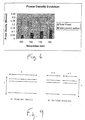
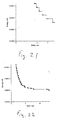
- Trade-offs are considered and combinations of costs and constraint values selected, e.g. combinations of power consumption and delay per unit length, leading to trade-off curves such as Pareto curves - see Fig. 1.
- at least back-end layers can be modeled but other layers can be included including packaging.
- additional geometrical parameters such as pitch/spacing can be included. Material related options can also be added and the trade-off, especially the Pareto curve concept can be used.
- these trade-off curves e.g. the interconnect Pareto curves have been integrated in a parameterized model of a component of the essentially digital system, for example in a model of a memory that reflects a cost/constraint combination, e.g. performance and energy consumption of an embedded SRAM for a 45nm technology node.
- the basis can be the CACTI model [14] it is preferred if this is significantly extended to allow for parameterization and to scale its internal models to 45 nm. All modem low-power memories are based on banking. Also the banking parameter that was present in CACTI can be been maintained but the important interbank interconnect contribution is preferably added.
- the third part is the evaluation of the behavior of the entire component of the essentially digital system, e.g. the entire memory organization in a telecommunications application, e.g. of a specific DAB application.
- This parameterized memory model can be used to explore the effect on the complete memory organization mapping decisions for a DAB decoder.
- the best strategy (at least for the L1 layer of a distributed shared memory, being the level directly above the register level) is to have each data variable in the application stored in its own memory. For practical reasons, such as testing though, usually that large number of memories is not feasible on chip.
- the intermemory interconnect becomes an important contributor too, as experiments have shown.
- the result is that some arrays have to be stored together.
- the problems that arise are twofold. Both the sizes and required access frequencies of the memories increase. The increased bandwidth is not such a problem in itself, since the total number of memory accesses cannot change. But, combined with the increased sizes, it results in the same number of accesses happening to larger, more power hungry memories.
- the two main phenomena that can cause major problems are bit-waste and arrays with very different access frequencies being stored together. Both of these lead to an increased energy consumption again. So clearly complex trade-offs are involved.
- Suitable exploration tools are available, e.g. the SBO-MAA tool set [15, 13]) extended to couple them to the adapted memory models. The result of these tools is a memory access schedule and corresponding memory organization.
- the real-time constraint for memory access times implied by this DAB implementation is 23.5ns. That is quite well achievable by all the memories within the available Pareto curve range of the SRAM model.
- process technology parameters at have been fixed and the banking parameter was explored.
- the exploration is carried out in accordance with the present invention, i.e. with the tools allowing the process technology parameters to vary, a global system energy gain of 30% is achieved.
- the system energy still depends on the number of RAMs that is allowed though (see Fig. 3). In this case the additional effect of adding Vdd scaling is negligible. But when more tight real-time constraints are added Vdd scaling also becomes important.
- the present invention makes use of the fact that process technology is able to provide varying physical dimensions of sub-components of essentially digital systems, e.g. the interconnect lines. So, even the same type of interconnect, i.e. local, can have wires with different dimensions on different parts of the chip. This means that process technology can provide an energy-delay tradeoff to system designers and can be exploited.
- circuit designers should be able to provide memories that work with a range of supply voltages.
- a range of different internal circuits e.g. sense amplifiers, can be of use.
- they can provide different versions of the same memory with different supply voltages.
- Banking cannot provide a sufficient range in energy-delay optimal tradeoff points, but it should always be exploited since it drastically improves both memory energy consumption and delay.
- components such as memories can be built that have not one cost-constraint operating point, e.g. an energy-delay operation point, but a broad range of such points.
- the varying aspect ratio of the interconnect can give a good range in delay and a smaller one in energy consumption.
- Vdd scaling gives good ranges in both energy and delay (at least in 130 nm technology).
- Inter-memory interconnect is another important aspect that cannot be solved by system designers alone. Activity on the system buses should be as low as possible and if possible it should take into account the length of the buses. But, layout and place and route decisions have a major impact on the power consumption of inter-memory interconnect. If this 'local' interconnect is very long then there is little system design can do to minimize their power consumption. Thus, this is a problem that requires collaboration and co-optimization between system design and placing and routing in physical design.
- inter-memory interconnect Another important conclusion is that if a good job is done in routing the inter-memory interconnect, then the power consumption is dominated by the energy consumed inside the memories. This intra-memory energy is dominated by the interconnect inside the memory, namely bitlines, wordlines and inter-bank interconnect To sum up, although inter-memory interconnect can be kept at low lengths and low power consumption, interconnect still dominates the overall power consumption of the memory organization.
- the present invention provides an apparatus having a processing unit co-operating with a first and a second essentially digital hardware device (EDHD), each of the first and second EDHDs being at least partly made by semiconductor processing and the manufacture of the first EDHD having at least one different semiconductor processing step compared with the manufacture of the second EDHD, the apparatus being for execution of a first and a second behavior, further comprising means for selecting one of the first and second EDHDs for execution of both the first and second behavior, each of the first and second EDHDs executing each of the first and second behaviors at a plurality of operating points belonging to a trade-off set, each operating point relating to a constraint-cost combination, wherein any first combination within the trade-off set is characterised in that all combinations within the trade-off set having a cost function with a lower cost value than the first combination have a higher value of the constraint than the first combination and wherein all combinations within the trade-off set having a value of the constraint lower than that of the first combination have
- the means for selecting may be implemented in an operating system of the apparatus.
- An EDHD can be any of a memory, microprocessor, co-processor, FPGA, PLA, PAL, a digital signal processing (DSP) circuit, pipeline, hardware accelerator, driver circuit, modem, I/O interface circuit, or combinations thereof
- DSP digital signal processing
- the trade-off set is preferably Pareto optimized.
- Matzke [9] describes the design problems that arise very well. In future technology nodes the part of the die that can be reached in one clock cycle will rapidly decrease. The reason is that wire performance cannot keep up with the increasing performance of transistors. As clock frequency increases rapidly and wire dimensions scale down, thus increasing RC delay, the length which a signal can travel in one clock cycle will be less than 10% of the die, in the near future.
- Wire delay is a problem that cannot be solved by system design directly, but while mapping an application to a given platform (large) latencies can be tolerated on most of the signal communications while still meeting all system-level timing constraints, as long as the mapping methodology has appropriate ways of dealing with this. So system designers can work around the performance problems too. One way to do this is by introducing data parallelism in the logic and allowing for larger communication delays to exist by pipelining locally and by increasing the latency and hence reducing the required clock frequency on large wires. A trade-off is involved with the buffer cost in that case, but by using a distributed memory hierarchy also that trade-off can be handled effectively to arrive at overall low power solutions meeting all real-time constraints. A trade-off differs from an optimization in that in a trade-off certain performance and/or design values become worse and some better. This results in various solutions with each solution having certain advantages and certain disadvantages.
- additional freedom in the design of sub-components e.g. wire dimensions that can be offered by process technology towards lower power consumption can be exploited by system designers, in order to reflect that reduction in a better cost function, e.g. lower total system power.
- the principle is that given the additional freedom, the silicon and the interconnect can be tailored to exactly meet the application requirements with minimum power consumption.
- the application domain is that of embedded multimedia and/or telecommunication systems.
- This context generally includes three large categories of applications: wireless/wired communications, network protocols and multimedia applications.
- Network applications include communication/network protocols like IP in the "edge" network.
- IP Internet Protocol
- the physical layer of the network becomes memory dominated, since it has to transfer data for multimedia applications that can be images or audio signals.
- Data for the operation and the administration of networks is also becoming very significant in volume. Examples are the turbo and Viterbi decoders, FFT in OFDM and SDMA matrix manipulations.
- the other category includes multimedia applications such as MPEG-2, MPEG-21, QSDPCM, JPEG2000 and so on.
- Applications of this sort typically require very large amounts of memory because they have to store image frames or other large objects. The result is that designs that are made for these applications are memory dominated. Additionally, most of the operations that are executed in these kind of applications are transformations on data and similar DSP like operations. This implies a large amount of memory accesses in order to fetch and store all the data. Due to the very large memory space that is required for these applications the largest part of the chips of such designs are usually occupied by memories. As a result, even in today's technology node, most of the power of the chips that are designed is consumed in the memories.
- Embodiments of the present invention will be focussed on memories and on minimising their energy consumption, however it should be understood that these are only examples of the present invention.
- the skilled person will appreciate that the present invention has wide application to any sort of essentially digital device, in particular those which are wire dominated, being defined as those wherein internal wirings contribute sufficiently to the global delay and energy consumption.
- on-chip embedded SRAMs have been selected. These are the memories that are currently used in designs and are expected to be used also in the near future. Embedded SDRAMs will also become important, but not for the 'local' memory layer. Activity on these memories can be kept low by Dynamic Memory Management and DTSE flows, but they will not be used as first layer memories. This fact emphasizes the need for on-chip memory hierarchy. In one aspect of the present invention, combinations of a constraint and a cost can be evaluated dependent upon changes in the processing technology used to make sub-components. As an example, the range in energy consumption and delay of interconnect that are provided by changing the physical dimensions of the wires is explored.
- the energy consumption of the system can be reduced significantly.
- Additional exploration ranges may be included, e.g. supply voltage.
- Current memories are designed to operate with a certain supply voltage. But in order to fine tune designs for power consumption memories that can operate with a range of supply voltages are preferred. Some memory libraries already provide this feature.
- Supply voltage scaling also provides a range in energy consumption and delay of memories. The rule of thumb is that such a change results in a trade-off- higher voltage means more energy consumption and less delay and vice versa. Two or three different designs of the same memory may be provided that operate with different supply voltages and delays.
- the present invention has at least different parts.
- the first part relates to building a model of a component of an essentially digital system, e.g. a model of memory that will reflect the performance of an embedded SRAM at a 45nm technology node. Having a memory model and feeding the ranges in interconnect dimensions and supply voltage conclusions can be made about how the performance and the energy consumption of a single memory are affected by these ranges.
- the second part is to evaluate the behaviour of the component, e.g. a memory architecture of a specific design. As an example a model to simulate the memory architecture of a design for a DAB decoder is described with the effects of the given ranges on it.
- the last part is to assess the impact of the sub-component design, e.g. inter-memory interconnect, or the buses that connect memories to functional units, on the power consumption of the design.
- the DAB decoder driver example has been already heavily optimised using the DTSE methodolgy. These optimisations are targeting low power operation and the main idea behind them is to minimise the number and the cost of memory accesses. Thus from a system design point of view, this driver has already been optimised as much as possible for a fixed process technology and memory bus library. Any further gains in power consumption come from the exploration of the ranges in interconnect dimensions and supply voltage are related to the application of the present invention.
- Another advantage of the DTSE optimisations is that they relax the real time constraints of the applications, mainly using software parallelism. The result is that it is possible to tradeoff relaxations on memory delay for lower power consumption.
- interconnect is classified into three different types, based on its length. Short interconnect of length smaller than 100um is considered local, interconnect longer than that but shorter than 1 mm is intermediate and wires longer than 1 mm are classified as global interconnect. These length limits are soft, but are determined by the distance a signal can travel on each type of interconnect in one clock cycle. Thus the limits are there, not because of manufacturing restrictions, but because of timing constraints. Methods exist to overcome these problems, i.e. using repeaters. But these methods come with a significant overhead and design complexity. Capacitance and resistance are assigned to the different wires based on their length. Application of the present invention can meet design constraints with a lower cost and shorter design time.
- An aspect of the present invention is to exploit the potential that is created for changing the physical dimensions of the wires between the different layers of the same interconnect type on the same chip. This can provide an opportunity for design time exploration in order to minimise global system-wide energy consumption.
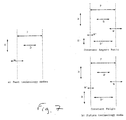
- Fig. 7 the different options that will exist for interconnect are shown along with today's case.
- the left hand side figure shows how interconnect is structured today.
- the wires of the same type on different layers have the same dimensions.
- P is the pitch and it is always constant for a certain type of interconnect.
- H is the height and W is the width of the wire.
- D is the distance between two adjacent wires of the same layer. All these parameters are very important for the calculation of energy consumption and delay on the wire.
- Energy which is proportional to capacitance depends heavily on D, since capacitance is inversely proportional to D. A small distance between the wire means large capacitance and vice versa.
- delay hand depends on capacitance and resistance of the metal lines. Resistance depends on the area of the cross-section of the wires, which is the product of height times width.
- Fig. 7 On the right hand of Fig. 7, the two different options for structuring interconnect in future nodes are shown.
- the flexibility that is added is that the physical dimensions of the lines between two layers of the same type can be different. For example, there can be fat intermediate interconnect on one metal layer and thin intermediate wires on the next.
- interconnect can be built that exactly matches application demands. Furthermore, there is no limit to only one interconnect choice for a complete design.
- different interconnect options for the different components of the design are explored and an optimal interconnect choice for each component that minimises a system-wide cost function can be selected.
- the attention is basically on a cost - energy consumption.
- cost-constraint trade-offs e.g. energy-delay tradeoffs for the interconnect can be explored. These tradeoffs are shown in Fig. 1, for the three types of interconnect.
- the pitch can vary across the different types of interconnect. For example, the pitch on the upper layers of a chip, which consists of global interconnect, is larger than the pitch of local interconnect.
- Fig. 5 shows the assumed organisation.
- the decoder first decodes the address and selects the appropriate row by driving one word-line in the data array.
- the array contains as many word-lines as rows in the memory matrix, but only one word-line in the matrix can go high at a time.
- Each memory cell along the selected row is associated with a pair of bit-lines; each bit-line is initially pre-charged high. When a word-line goes high, each memory cell determines which bit-line it should drive low. It is important to note here that in every access to this memory all the bit-lines, in a single plane or matrix, are activated.
- Each sense amplifier monitors a pair of bit-lines and detects when one changes. By detecting which line goes low, the sense amplifier can determine which logical value was stored in the memory cell. It is possible for one sense amplifier to be shared among several pairs of bit-lines. In this case, a multiplexer is inserted before the sense amplifiers; the select lines of the multiplexor are driven by the decoder. The number of bit-lines that share a sense amplifier depends on the layout parameters described later.
- the CACTI model (enhanced Cache Access and Cycle TIme model) [14] [21] is a cache simulator that was developed for the investigation and comparison of different cache organisations. It includes analytical models for every different cache component and calculates their delay and energy consumption by decomposing them to simple RC models. It claims very high accuracy compared to HSPICE simulations.
- Ndwl is the number of split word-lines
- Ndbl is the number of split bit-lines.
- the number of banks, or smaller matrices, is the product of Ndwl times Ndbl.
- CACTI explores banking is that both delay and energy consumption are reduced. Having smaller matrices means that the length of the word-lines and the bit-lines will be shorter than that of the original lines. Since both energy consumption and delay of metal lines is proportional to the length of the line, shorter lines result in reducing both.
- banking introduces overhead such as periphery and inter-bank line effects, along with an area overhead. At some point, these effects should start cancelling any gains achieved by further banking. Unfortunately, this overhead is not modelled in CACTI.
- Nspd Another parameter that is used by the CACTI model is Nspd. This parameter is the number of blocks that are mapped to a single cache line. It has a large impact on the delay and the energy consumption of the smaller matrices since it alters their 'shape', thus changing again the lengths of the bit-lines and the word-lines. Apart from that, also the architecture of the cache is affected, because block size is a major cache characteristic. One other effect that this parameter has, is making the matrices more square, if well chosen. Usually the word depth of a memory (and cache) is much larger than its bitwidth. By applying this parameter the model tries to make the matrices more square, than long and narrow, so that they are more feasible to implement and the length of the bit-lines is reduced.
- CACTI uses a cost formula that takes into account delay and energy consumption.
- Energy in the formula denotes the energy per access for the architecture being explored, the same apply for delay.
- Maximum energy and maximum delay denote the absolute maximum values of energy per access and access time for any combination of the parameters explored. Most of the times these maximum values come from the un-banked case.
- This model can be scaled to different technology nodes. It was originally built for the 800nm technology node and it offers the potential of scaling down to the 100nm technology node.
- the supply voltages that result for the different technology nodes are shown in Table 2.
- the CACTI model is a start but is compensated for its shortcomings plus adding some more functionality to it.
- the exploration of banking schemes the exploration of the effect of different interconnect aspect ratios and Vdd scaling on the memories is provided.
- the search space is extended, from the space of all the banking schemes, to the larger space that includes all possible combinations of banking, aspect ratios and Vdd choices.
- Another major modification to the functionality of the model was to change the output from the energy-delay pair that minimises a cost function for each memory, to the set of all energy-delay optimal results.
- a single lowest energy consuming or lowest delay operating point is not what is required but rather all the usuable operating points.
- a number of operating points that are optimal is determined, so that later there is a freedom to decide which one suits the application better and thus to use that one. So instead of a single point in the energy-delay space, the output of the model is a trade-off cruve, e.g. a Pareto curve, like the one in Fig. 11.
- a trade-off curve, of which a Pareto curve is one example, is the boundary between solutions whose feasibility is not very practical and solutions that are not optimal.
- the points of the Pareto curve are the optimal energy-delay solutions. There are no points that can have lower energy consumption and smaller delay than any of the Pareto points, otherwise they would be Pareto points themselves.
- Nspd remains in the model, even though caches are not veing considered. This parameter also played the role of a 'squaring factor'. This means that exploring Nspd enables finding the best combination of memory height and width that minimises memory delay and energy consumption. Actually, Nspd will directly affect the relative dimensions of banks inside the memory, so it is the optimal combination ofNdwl, Ndbl and Nspd that should be found.
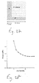
- Fig. 12 the energy consumption of the different memory components that is predicted by the CACTI model is shown as a percentage over the total memory consumption.
- the components that are shown here correspond to Fig. 8.
- the output driver, which is not shown, has very small consumption, less than 1%.
- the 350 nm technology node was used for these experiments.
- the multiplexers are assumed to be part of the sense amplifiers.
- bit-lines and word-lines behave differently. Bit-lines have a large contribution in energy consumption and a negligible contribution in delay. On the other hand, word-lines contribute significant delay, but consume negligible energy. The reason is that all the bit-lines are activated during decoding, so the energy consumed is high, but there is almost no delay. For word-lines it is the opposite, only one word-line is activated, but it has to drive a large number of transistors, which leads to an increased delay and a small energy consumption.
- Figs. 14 and 15 show how the delay and the energy consumption of the different components evolves through the different technology nodes.
- the CACTI model predicts that the proportion of delay contributed by each component will not change significantly for the technology nodes down to 100nm. This, however, is not true, because the trend, even nowadays, is that interconnect delay is becoming ever more significant, while the delay of silicon parts is becoming relatively smaller [8].
- the model fails to take into account the current trends. It is more realistic to assume that in the future the wires will increase their delay contribution. This is caused by the fact that scaling down transistors generally results in smaller transistor delay, but scaling wires increases the delay because of the increased resistance of the wire, as discussed previously.
- inter bank interconnect internal memory buses that connect the different banks to the memory ports
- Evans et al. [17] provides another idea of contribution breakdown for energy.
- the contribution of the decoder, along with the data latches and the wordline drivers is about 60%.
- Another 30% is added by the bitlines and the output driver contributes again 1% of energy consumption.
- the surprise comes from the sense amplifiers which contribute negligible energy. Apart from the sense amps, the rest of the percentages are quite reasonable and agree with CACTI's, since the memory considered in the paper is a 4Mbit memory for the 2 micron technology node.
- decoders and output drivers are digital circuits that are expected to have reduced contributions for the 45nm node. Therefore, it is assumed that the decoder will contribute 10% of delay and energy, while the output drivers will contribute about 10% of delay, but will remain very efficient in energy consumption contribution staying at about 1%.
- banked memories should have internal buses that are quite long.
- a memory that is not banked can have the port of the matrix directly connected to the memory port, without any additional wiring.
- Memories that are banked need to have some internal bus lines that connect the memory address port to the bank decoders and the multiplexer output to the data port of the memory.
- These internal buses can be very long, much longer than the bit-lines and each bus consists of several wires.
- each memory access the delays of these two buses are added, they cannot overlap. Therefore, they should be modelled, since they are expected to contribute a lot to overall energy consumption and delay.
- This floorplan should include inter-bank wires, but it should also include a model of the area overhead that banking introduces. The reason is that the length of the inter-bank lines is heavily influenced by the total memory area.
- the floorplan chosen in the model is shown in Fig. 16.
- the number of bank rows (BR) and bank columns (BC) are:
- the shortest lines inside the memory are the word-lines and the bit-lines. Although these lines can have lengths up to a few hundred of microns, for small and medium sized memories they seldom exceed 100 micron. Their length is very much dependent on the banking scheme that is chosen. As a result, bit-lines and word-lines have been classified into the local interconnect category.
- the inter-bank line issue is different. Their length is usually in the range of intermediate interconnect and rarely is their length lower than 100um or larger than 1mm. These lines are, therefore, considered as intermediate interconnect.
- the swing voltage is equal to the supply voltage.
- These components include the word-lines and all the logic components of the memory, such as the decoder and output drivers.
- the sense amplifiers have no swing voltage associated with them, since they are not fully modelled.
- the only component that has a lower swing voltage are the bit-lines, where it is 66% of the supply voltage. That holds only for the line and not the transistors connected to the line, which still have swing equal to the supply voltage.
- Rambus [20] which includes an off-chip connection between the SDRAM and the processor on a PC motherboard. On this connection they have managed to keep the swing voltage to 200mV, which a rather low value considering it is off-chip and the supply voltage is 3.3V.
- a frame-buffer SRAM is used on a low power chipset.
- the swing voltage on the bit-lines of the frame-buffer can be kept at 350mV with a 1.1 V supply voltage.
- bit-lines can work with a lower swing voltage, because they are short and the signal will not have problems transmitting across the line. Especially if it is assumed that the sense amplifiers are placed on the output of each bank, this voltage is a reasonable choice.
- the inter-bank lines need a higher swing voltage because they have to 'carry' the signal for a larger distance.
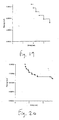
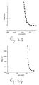
- Fig. 14 only banking is explored. This curve corresponds to a 64kbit memory with a bitwidth of 8. This memory instance is used throughout these experiments.
- the supply voltage was assumed to be 0.5V and the fast and power hungry interconnect aspect ratio option has been adopted.
- Fig. 18 the impact of exploring the different options for the interconnect aspect ratio is shown. To do this exploration all the different possibilities were taken into account. There are four options for the inter-bank lines and four options for the bit-lines and the word-lines, since they belong to different types of interconnect. The combination of these two orthogonal explorations is shown in Fig. 18. The supply voltage used is 0.5V, while the banking used is the most energy efficient.
- the range of values for capacitance and RC delay that is provided by the interconnect options is reflected in the energy-delay Pareto curve of the memory.
- the Pareto curve has points that range roughly from 0.08 to 0.05 pJ in energy consumption and from 4 to 15 nsecs in delay. These values correspond to energy consumption and delay per access. From Table 2 it can be seen that the ranges in energy and delay for the interconnect were about 1.5 and 4 respectively. This means that changing the choice of interconnect parameters has a direct and almost linear impact on the performance of the memory.
- Another conclusion is that the different aspect ratio options mainly affect the memory delay, since they provide a large range in delay, a factor 4, and a smaller range in energy consumption, a factor 1.5 roughly. The result is that going to lowest possible energy consumption means paying a big price in delay.
- Scaling the supply voltage has a similar impact on energy consumption of the memory and delay. As described above, energy consumption is proportional to the supply voltage. But, delay is also proportional to the supply voltage since it is scaled from the reference voltage.
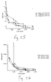
- Fig. 20 shows the result of exploring the banking schemes along with the different aspect ratio options.
- the two points on the right are useful only in the case of very relaxed timing constraints, where the delay sacrificed for such a small gain in energy is acceptable.
- the other points provide plenty of energy-delay solutions for a designer to use in order to globally optimise the performance of the memory architecture.
- this curve half of the points use a supply voltage of 0.5V and the other half resort to larger voltages to further reduce their delay.
- the minimum delay which can be achieved with 0.5V is 3.6 nsecs. If that delay does not satisfy the global system timing constraint then the supply voltage should be increased, thus increasing the energy consumption more rapidly.
- Fig. 23 an area-delay Pareto curve is shown.
- no limit is placed on the energy consumption.
- the points that have less than maximum area are not banked to the limit, thus they are not energy efficient.
- Fig. 24 shows the energy-area Pareto curve of the same memory. There is no limit on the memory delay. The conclusion that can be drawn from this curve is the same as the one made earlier. Exploring banking schemes is not useful if area is not really critical in the design. The gains in energy consumption from banking to the limit are obvious (more than a factor 10), while the overhead of area is not that important (about 50%).
- Fig. 25 shows several area-delay Pareto curves, where the energy consumption is bounded to certain limits. It becomes clear that if area is important for the design, then it can be traded-off for delay.
- Fig. 26 is similar to the previous, but it is an energy-area Pareto curve with the delay within bounds. From this figure one can trade-off area for energy.
- the power consumption of a memory organisation depends on two parameters.
- the energy consumption per access of a memory is directly linked with its size. Of course, many other factors have an influence. To minimise the energy, one has to keep the size as small as possible. On the other hand, the access frequency of each array is dictated by the application.
- Bit-waste occurs when two arrays with different bitwidth are stored in the same memory.
- the memory has to be wide enough to accommodate the wide array, but as a result the narrow array cannot fill the remaining width, see Fig. 27.
- a DAB broadcaster is able to provide either six high quality radio programs with associated data, or for instance one MPEG lvideo signal.
- DAB provides any combination of services up to a total of about 1.8Mb/s. It uses Orthogonal Frequency Division Multiplex (OFDM) modulation scheme which is resistant against multi path interference and frequency-selective fading.
- OFDM Orthogonal Frequency Division Multiplex
- the OFDM scheme contains up to 1536 carriers for terrestrial broadcasting (Mode I) and is implemented in the FFT processor.
- the channel coding is based on a convolutional code with constraint length 7 and a maximum redundancy factor of 4 (lowered by puncturing).
- DTS heavy data transfer and storage optimised version of the DAB decoder [22] has been used for the experiments.
- the optimisations applied focus mainly on reducing the power consumption of the implementation of this decoder by removing redundant accesses in the global data-flow transformation step and by improving access regularity and locality in the global loop trafo step.
- the access times for the various arrays have been globally optimised for power consumption.
- One major optimisation is that accesses to the two larger arrays of the application have been software pipelined, allowing these memories to have an access time four times larger than that of the smaller arrays. This will allows to measure the effect of banking, interconnect aspect ratio and Vdd scaling on an already heavily optimised design.
- the optimisations that were applied also resulted in making the real-time constraint for the access times of the memories easier to meet.
- the DTS optimized version of the DAB decoder uses 22 arrays. Seven of them are stored in ROMs, while the other 15 have to be assigned to SRAMs. Although we will not mention these 7 arrays or the ROMs further in this chapter, it should be noted that all the calculations and the figures include them. The reason they are not mentioned is that their contribution in power consumption is negligible. The remaining 15 arrays are the ones that consume almost all the power. Their sizes vary a lot. Two arrays are very larger than the other, one is 128kbit and the other is 512kbit. The rest of the arrays do not exceed 80kbit in total, one is 40kbit, two are about 10kbit and the rest are quite smaller. Another important metric of the arrays is their access frequencies.
- the two large arrays have obviously been optimised to have few accesses and as a result, for the 512kbit array the access frequency is 0.3 Maccesses per sec, while for the 128kbit it is 0.17 Maccesses per sec.
- the 40kbit array is accessed 3 million times per sec and the 10kbit ones about 1 million. It becomes clear that even though two arrays dominate total memory size, their power contribution will not dominate overall power consumption, because of their reduced access frequencies. In a balanced design (DTSE optimized), this should always be the case.
- a memory library is built that meets certain timing constraints.
- a memory library is a collection of cost -constraint value pairs or combinations, e.g. energy-area value pairs of memories of various sizes that have an access time smaller than the constraint.
- use will be made of the actual real time constraint of the DAB decoder, which is 23.5ns for each memory access.
- the two large arrays of the application are allowed to have 4 times as much access time due to software parallelism. Thus, and due to their size, they will be stored in two memories alone, otherwise this advantage cannot be exploited. If something else is stored with them then the memories would have to be able to achieve the 23.5ns access time. This is also the reason why the minimum number of memories is large. At least three memories are needed so that no conflicts exist between accesses in the other arrays and two memories for the large arrays.
- Each memory is banked as much as possible, to locally reduce energy consumption and delay, and uses the fast, but energy hungry aspect ratio.
- the reason this interconnect is used here is that general-purpose microprocessors, which drive technology, are not really power conscious designs.
- Fig. 28 shows the trend expected for power. The more memories there are, the less power is consumed. Of course at some point the power consumption converges to the minimum possible value, which is encountered at the maximum number of memories or at the point where the inter-memory interconnect starts to become a significant contributor.
- Fig. 29 shows the effect of using a more energy efficient aspect ratio. This figure was generated sing a memory library that explored banking and interconnect aspect ratios for the 23.5ns real time constraint. Comparing Figs. 28 and 29 one can see that a significant reduction of power consumption can be achieved by using slower, but more energy efficient interconnect. The reason one can do that is because careful application design and optimisations have led to a quite loose timing constraint that memories can very easily meet. As a result, memories can tradeoff remaining, unused, speed for improved energy consumption, minimising overall power consumption of the application. The gain that can be achieved in this way is significant, since there is a reduction from 0.8nW to 0.52nW, about 30%, for the maximum number of memories.
- Fig. 30 shows the effects of using all possible explorations for individual memories, namely banking, aspect ratio options and Vdd scaling. It was expected that this curve would be the same as the one without the exploration of Vdd. Using Vdd values other than the absolute minimum, is only necessary in order to increase memory speed at the expense of energy consumption. Since the timing constraint is very loose, there is no reason to increase the supply voltage of the memories.
- Fig. 31 show the resulting power consumption when Vdd scaling and banking are explored.
- the impact of increasing the Vdd is very clear, the minimum power consumption has risen to 0.9 1 nW. So, it is clear that one can tradeoff power for delay, if the design requirements are too difficult for the memories to achieve otherwise.
- Inter-memory interconnect consists of the buses that connect the memories to the functional units or to other memories. It is quite difficult to predict how much impact inter-memory interconnect is going to have on the power of a certain design, because it heavily depends on the floorplan and the placing and routing. The energy consumption of this interconnect depends on four things. Capacitance of the wires, voltage (supply and swing), activity and length.
- inter-memory interconnect uses the lowest capacitance possible.
- the buses will be assigned capacitance and RC values according to their length. Shorter buses will be considered as intermediate interconnect, while longer will be treated as global. This decision is in line with the lengths predicted by the ITRS roadmap [8].
- the experiments done for the inter-memory interconnect were carried out on the same driver as the previous ones, the DAB decoder.
- the first step of these experiments is to define the memory architecture. It has been seen in the previous chapter that the DAB uses two large arrays that have looser time constraints and a number of smaller arrays. Thus, it makes sense to use a layered architecture, where the two large arrays will be stored in two memories in the second layer and the rest of the arrays will be stored in a number of first layer memories.
- the second layer memories are referred to as global and the first layer memories as local.
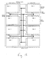
- Fig. 4 shows what this architecture looks like.
- An architecture with 8 local and 2 global memories is shown.
- the exploration degree of freedom in these experiments will be the number of local memories. This together with the allocation and assignment of arrays to memories dictates the bus activity. It does not make sense to play with the number of global memories, since the driver application pretty much defines the architecture. It is interesting, though, to note that if a one layer approach was used buses of local memories could become much longer, increasing power consumption.
- This figure also shows a routing possibility for the inter-memory interconnect. The assumption we have made when choosing this routing was that the memories will not have to communicate directly with each other. The data will have to go from the memories to the functional unit and then back to the memories. This assumption holds for the DAB application, so the experiments were made on this architecture.
- each memory has its own dedicated bus.
- the alternative of bus sharing is not considered because it only benefits in terms of area. Sharing a common bus is not beneficial for power consumption, because it cannot reduce the number of lines that are active. Having dedicated buses means that one does not use more lines than necessary, even though the total number of wires is very increased. For delay the two options are similar, bus sharing may introduce some small delay due to switches that are required.
- the lengths of the buses depend on the area that the memories occupy. This means that, because the buses have to pass across a number of memories, changing the area of the memories results in a change in the physical length of the lines.
- minimum length buses are desirable to have the most activity and the longer the buses are the less activity they should have. This is also in line with assigning the large and not frequently accessed arrays of the application on the second layer of the architecture.
- Fig. 35 the power consumption of the memories and the inter-memory interconnect is shown. This experiment was done for the actual real-time constraint of the DAB application. The delay of the inter-memory interconnect, though, has not been taken into account for the appropriate selection of the speed of the memories. So 23.5ns is the time in which the memory has to respond from the time it received the command, not the time between the functional unit issuing the command and getting the data. But, given the fact that the constraint is very loose this does not affect the outcome.
- interconnect The power contribution of the interconnect is kept very low, at 11 memories it is 16% of the total consumption. This means that inter-memory interconnect does not seem to be the bottleneck.
- present invention includes altering the run-time behavior of an essentially digital system by selecting one of one or more hardware components, each of which is able to carry bout the same tasks.
- present invention includes an apparatus having a processing unit, for example a microprocessor or an FPGA, PAL, PLA or similar.
- the processing unit may be embedded, e.g. on a PCB or in an accelerator or in a specific module which is provided within a larger apparatus such as a personal computer, a mobile phone, a PDA.
- the processor co-operates with a first and a second essentially digital hardware device (EDHD). These two devices have preferably been optimized by the methods explained above.
- Each of the first and second EDHDs are at least partly made by semiconductor processing and the manufacture of the first EDHD have at least one different semiconductor processing step compared with the manufacture of the second EDHD.
- the term "different semiconductor processing step" as used in this specification and attached claims includes a layout change (like another width of a line) or use of a different processing parameter.
- the semiconductor step which is different could be any of forming a conducting line width and/or length, using a material for a conductive or an insulating element, forming an aspect ratio of a conducting element, doping a semiconductor region, forming a transistor gate length, forming a transistor gate oxide thickness, forming spacing of conducting elements, or combinations thereof.
- These steps alter the properties of a sub-component which is comprised within the EDHD and alter the constraint-cost pair behavior of that device.
- the apparatus is for execution of a first and a second behavior, such as for example displaying a visible image or reproducing a audio tone, coding or encoding a digital bit stream or digital data, compressing or decompressing a digital bit stream or digital data, modulation or demodulation of a signal, for example in a telecommunications application.
- a redundancy is provided in the hardware of the apparatus.
- These two hardware devise are not exactly equivalent as they are each made with a different technology.
- the two devices differ from normal redundancy, for example, of memories which is provided for safety critical application.
- the two devices due to their different sub-component performances are able to perform differently with respect to different tasks. This may result in a trade-off.
- device 1 when executing task 1, may have a lower cost function (e.g. uses less energy) but a higher constraint value (e.g. take more time to execute) than device 2.
- a higher cost function e.g. uses more energy
- a lower constraint value e.g. takes less time to execute
- the apparatus preferably has means for selecting one of the first and second EDHDs for execution of both the first and second behavior, e.g. at run-time. From the above description it can be said that each of the first and second EDHDs executes each of the first and second behaviors at a plurality of operating points belonging to a trade-off set, each operating point relating to a constraint-cost combination, wherein any first combination within the trade-off set is characterized in that all combinations within the trade-off set having a cost function with a lower cost value than the first combination have a higher value of the constraint than the first combination and wherein all combinations within the trade-off set having a value of the constraint lower than that of the first combination have a higher value of the cost function than that of the first combination.
- the trade-off is preferably Pareto optimised.
- the operating system of the essentially digital device is adapted to include the selection means.
Landscapes
- Engineering & Computer Science (AREA)
- Computer Hardware Design (AREA)
- Physics & Mathematics (AREA)
- Theoretical Computer Science (AREA)
- Evolutionary Computation (AREA)
- Geometry (AREA)
- General Engineering & Computer Science (AREA)
- General Physics & Mathematics (AREA)
- Design And Manufacture Of Integrated Circuits (AREA)
Priority Applications (1)
| Application Number | Priority Date | Filing Date | Title |
|---|---|---|---|
| EP04075934A EP1467294A3 (de) | 2003-04-04 | 2004-03-25 | Verfahren zum Entwurf elektronischer Systeme unter Verwendung einer Bibliothek von Hardware-Komponenten mit Leistungsparametern und Kostfunktionen |
Applications Claiming Priority (3)
| Application Number | Priority Date | Filing Date | Title |
|---|---|---|---|
| EP03447082 | 2003-04-04 | ||
| EP03447082 | 2003-04-04 | ||
| EP04075934A EP1467294A3 (de) | 2003-04-04 | 2004-03-25 | Verfahren zum Entwurf elektronischer Systeme unter Verwendung einer Bibliothek von Hardware-Komponenten mit Leistungsparametern und Kostfunktionen |
Publications (2)
| Publication Number | Publication Date |
|---|---|
| EP1467294A2 true EP1467294A2 (de) | 2004-10-13 |
| EP1467294A3 EP1467294A3 (de) | 2005-06-01 |
Family
ID=34130439
Family Applications (1)
| Application Number | Title | Priority Date | Filing Date |
|---|---|---|---|
| EP04075934A Withdrawn EP1467294A3 (de) | 2003-04-04 | 2004-03-25 | Verfahren zum Entwurf elektronischer Systeme unter Verwendung einer Bibliothek von Hardware-Komponenten mit Leistungsparametern und Kostfunktionen |
Country Status (2)
| Country | Link |
|---|---|
| US (1) | US7124377B2 (de) |
| EP (1) | EP1467294A3 (de) |
Cited By (1)
| Publication number | Priority date | Publication date | Assignee | Title |
|---|---|---|---|---|
| US8578319B2 (en) | 2004-03-30 | 2013-11-05 | Imec | Method and apparatus for designing and manufacturing electronic circuits subject to process variations |
Families Citing this family (29)
| Publication number | Priority date | Publication date | Assignee | Title |
|---|---|---|---|---|
| US8554601B1 (en) | 2003-08-22 | 2013-10-08 | Amazon Technologies, Inc. | Managing content based on reputation |
| US7530047B2 (en) * | 2003-09-19 | 2009-05-05 | Cadence Design Systems, Inc. | Optimized mapping of an integrated circuit design to multiple cell libraries during a single synthesis pass |
| JP4065229B2 (ja) * | 2003-11-26 | 2008-03-19 | 松下電器産業株式会社 | 半導体集積回路の電源ノイズ解析方法 |
| US7082064B2 (en) * | 2004-01-29 | 2006-07-25 | Micron Technology, Inc. | Individual I/O modulation in memory devices |
| US7308664B1 (en) | 2004-02-09 | 2007-12-11 | Altera Corporation | Method and apparatus for utilizing long-path and short-path timing constraints in an electronic-design-automation tool for routing |
| US7207020B1 (en) * | 2004-02-09 | 2007-04-17 | Altera Corporation | Method and apparatus for utilizing long-path and short-path timing constraints in an electronic-design-automation tool |
| US7363601B2 (en) * | 2004-10-15 | 2008-04-22 | International Business Machines Corporation | Integrated circuit selective scaling |
| KR100688525B1 (ko) * | 2005-01-26 | 2007-03-02 | 삼성전자주식회사 | 이벤트 구동 스위치 레벨 시뮬레이션 방법 및 시뮬레이터 |
| US7653519B1 (en) * | 2006-04-13 | 2010-01-26 | Cadence Design Systems, Inc. | Method and mechanism for modeling interconnect structures for integrated circuits |
| US7802219B2 (en) * | 2006-11-30 | 2010-09-21 | Cadence Design Systems, Inc. | Flat placement of cells on non-integer multiple height rows in a digital integrated circuit layout |
| JP2008204349A (ja) * | 2007-02-22 | 2008-09-04 | Fujitsu Ltd | レイアウト設計プログラム、該プログラムを記録した記録媒体、レイアウト設計方法、およびレイアウト設計装置 |
| US8027938B1 (en) * | 2007-03-26 | 2011-09-27 | Google Inc. | Discriminative training in machine learning |
| US20090070716A1 (en) * | 2007-09-12 | 2009-03-12 | Joshi Rajiv V | System and method for optimization and predication of variability and yield in integrated ciruits |
| US9087164B2 (en) | 2008-01-26 | 2015-07-21 | National Semiconductor Corporation | Visualization of tradeoffs between circuit designs |
| US7966588B1 (en) * | 2008-01-26 | 2011-06-21 | National Semiconductor Corporation | Optimization of electrical circuits |
| US7873938B2 (en) * | 2008-06-27 | 2011-01-18 | Transwitch Corporation | Method for constructing a variable bitwidth video processor |
| US8296710B2 (en) * | 2009-07-28 | 2012-10-23 | Xilinx, Inc. | Soft constraints in scheduling |
| US8819208B2 (en) | 2010-03-05 | 2014-08-26 | Solidfire, Inc. | Data deletion in a distributed data storage system |
| US9054992B2 (en) | 2011-12-27 | 2015-06-09 | Solidfire, Inc. | Quality of service policy sets |
| US9838269B2 (en) | 2011-12-27 | 2017-12-05 | Netapp, Inc. | Proportional quality of service based on client usage and system metrics |
| US10133557B1 (en) * | 2013-01-11 | 2018-11-20 | Mentor Graphics Corporation | Modifying code to reduce redundant or unnecessary power usage |
| US20150244795A1 (en) | 2014-02-21 | 2015-08-27 | Solidfire, Inc. | Data syncing in a distributed system |
| US20160077945A1 (en) * | 2014-09-11 | 2016-03-17 | Netapp, Inc. | Storage system statistical data storage and analysis |
| US10133511B2 (en) | 2014-09-12 | 2018-11-20 | Netapp, Inc | Optimized segment cleaning technique |
| US9836229B2 (en) | 2014-11-18 | 2017-12-05 | Netapp, Inc. | N-way merge technique for updating volume metadata in a storage I/O stack |
| US9798847B2 (en) * | 2015-07-07 | 2017-10-24 | International Business Machines Corporation | Cross-hierarchy interconnect adjustment for power recovery |
| US10929022B2 (en) | 2016-04-25 | 2021-02-23 | Netapp. Inc. | Space savings reporting for storage system supporting snapshot and clones |
| US10642763B2 (en) | 2016-09-20 | 2020-05-05 | Netapp, Inc. | Quality of service policy sets |
| TWI627521B (zh) | 2017-06-07 | 2018-06-21 | 財團法人工業技術研究院 | 時序估算方法與模擬裝置 |
Family Cites Families (5)
| Publication number | Priority date | Publication date | Assignee | Title |
|---|---|---|---|---|
| US5870313A (en) * | 1994-04-19 | 1999-02-09 | Lsi Logic Corporation | Optimization processing for integrated circuit physical design automation system using parallel moving windows |
| US6862563B1 (en) * | 1998-10-14 | 2005-03-01 | Arc International | Method and apparatus for managing the configuration and functionality of a semiconductor design |
| US7117455B2 (en) * | 2003-07-24 | 2006-10-03 | International Business Machines Corporation | System and method for derivative-free optimization of electrical circuits |
| US7725848B2 (en) * | 2005-01-27 | 2010-05-25 | Wolfgang Nebel | Predictable design of low power systems by pre-implementation estimation and optimization |
| US8799830B2 (en) * | 2004-05-07 | 2014-08-05 | Mentor Graphics Corporation | Integrated circuit layout design methodology with process variation bands |
-
2004
- 2004-03-25 EP EP04075934A patent/EP1467294A3/de not_active Withdrawn
- 2004-04-02 US US10/817,310 patent/US7124377B2/en not_active Expired - Lifetime
Non-Patent Citations (6)
| Title |
|---|
| BROCKMEYER E ET AL: "Systematic cycle budget versus system power trade-off: a new perspective on system exploration of real-time data-dominated applications" LOW POWER ELECTRONICS AND DESIGN, 2000. ISLPED '00. PROCEEDINGS OF THE 2000 INTERNATIONAL SYMPOSIUM ON JULY 26-27, 2000, PISCATAWAY, NJ, USA,IEEE, 26 July 2000 (2000-07-26), pages 137-142, XP010517318 ISBN: 1-58113-190-9 * |
| GIVARGIS T ET AL: "System-level exploration for Pareto-optimal configurations in parameterized systems-on-a-chip" IEEE/ACM INTERNATIONAL CONFERENCE ON COMPUTER AIDED DESIGN. ICCAD 2001. IEEE/ACM DIGEST OF TECHNICAL PAPERS (CAT. NO.01CH37281) IEEE PISCATAWAY, NJ, USA, 8 November 2001 (2001-11-08), pages 25-30, XP002323201 ISBN: 0-7803-7247-6 * |
| GRUN P ET AL: "Memory system connectivity exploration" PROCEEDINGS 2002 DESIGN, AUTOMATION AND TEST IN EUROPE CONFERENCE AND EXHIBITION IEEE COMPUT. SOC LOS ALAMITOS, CA, USA, 4 March 2002 (2002-03-04), pages 894-901, XP002323202 ISBN: 0-7695-1471-5 * |
| PAPANIKOLAOU A ET AL: "Global Interconnect Trade-off For Technology Over Memory Modules To Application Level: Case Study" INT. WORKSHOP SYST. LEVEL INTERCONNECT PREDICT.; INTERNATIONAL WORKSHOP ON SYSTEM LEVEL INTERCONNECT PREDICTION 2003, 2003, pages 125-132, XP002323252 * |
| PAPANIKOLAOU A ET AL: "Interconnect Exploration for Future Wire Dominated Technologies" INT. WORKSHOP SYST. LEVEL INTERCONNECT PREDICT.; INTERNATIONAL WORKSHOP ON SYSTEM LEVEL INTERCONNECT PREDICTION 2002, 2002, pages 105-106, XP002323203 * |
| YUNSI FEI ET AL: "Functional partitioning for low power distributed systems of systems-on-a-chip" DESIGN AUTOMATION CONFERENCE, 2002. PROCEEDINGS OF ASP-DAC 2002. 7TH ASIA AND SOUTH PACIFIC AND THE 15TH INTERNATIONAL CONFERENCE ON VLSI DESIGN. PROCEEDINGS. BANGALORE, INDIA 7-11 JAN. 2002, LOS ALAMITOS, CA, USA,IEEE COMPUT. SOC, US, 7 January 2002 (2002-01-07), pages 274-281, XP010588114 ISBN: 0-7695-1441-3 * |
Cited By (1)
| Publication number | Priority date | Publication date | Assignee | Title |
|---|---|---|---|---|
| US8578319B2 (en) | 2004-03-30 | 2013-11-05 | Imec | Method and apparatus for designing and manufacturing electronic circuits subject to process variations |
Also Published As
| Publication number | Publication date |
|---|---|
| EP1467294A3 (de) | 2005-06-01 |
| US20050039156A1 (en) | 2005-02-17 |
| US7124377B2 (en) | 2006-10-17 |
Similar Documents
| Publication | Publication Date | Title |
|---|---|---|
| US7124377B2 (en) | Design method for essentially digital systems and components thereof and essentially digital systems made in accordance with the method | |
| Tsai et al. | Three-dimensional cache design exploration using 3DCacti | |
| Balfour et al. | Design tradeoffs for tiled CMP on-chip networks | |
| Thoziyoor et al. | CACTI 5.1 | |
| CN103314378B (zh) | 智能存储器系统编译器 | |
| US8578319B2 (en) | Method and apparatus for designing and manufacturing electronic circuits subject to process variations | |
| Puttaswamy et al. | 3D-integrated SRAM components for high-performance microprocessors | |
| US8578312B2 (en) | Method and apparatus for designing and manufacturing electronic circuits subject to leakage problems caused by temperature variations and/or aging | |
| Paul et al. | MAHA: An energy-efficient malleable hardware accelerator for data-intensive applications | |
| Shukla et al. | Tread-m3d: Temperature-aware dnn accelerators for monolithic 3-d mobile systems | |
| Fadnavis et al. | PNR flow methodology for congestion optimization using different macro placement strategies of DDR memories | |
| Paul et al. | Energy-efficient hardware acceleration through computing in the memory | |
| Shiue et al. | Multi-module multi-port memory design for low power embedded systems | |
| Dorostkar et al. | Low‐power heterogeneous uncore architecture for future 3D chip‐multiprocessors | |
| Koob et al. | Design of a 3-D fully depleted SOI computational RAM | |
| EP1607887A2 (de) | Energiebewusste konfigurierbare Treiberschaltunge für an einer Belastung angeschlossenen Leitung | |
| Papanikolaou et al. | Global interconnect trade-off for technology over memory modules to application level: case study | |
| Milojevic et al. | Pathfinding: A design methodology for fast exploration and optimisation of 3D-stacked integrated circuits | |
| Zeng et al. | Memory performance prediction for high-performance microprocessors at deep submicrometer technologies | |
| Wu et al. | Exploiting the Memory-Compute-Coupling Feature for CIM Accelerator Design Optimization | |
| Randall | Cost-Driven Integration Architectures for Multi-Die Silicon Systems | |
| EP1583009A1 (de) | Verfahren und Vorrichtung zum Entwerfen und Herstellen von elektronischen Schaltungen abhängig von Prozessveränderungen | |
| DeHon | Wordwidth, instructions, looping, and virtualization: the role of sharing in absolute energy minimization | |
| Chua | An FPGA memory architecture to enable efficient weight implementations for machine learning applications | |
| Nandakumar | Physically-Aware Architectural Exploration and Solutions for Heterogeneous Processors |
Legal Events
| Date | Code | Title | Description |
|---|---|---|---|
| PUAI | Public reference made under article 153(3) epc to a published international application that has entered the european phase |
Free format text: ORIGINAL CODE: 0009012 |
|
| AK | Designated contracting states |
Kind code of ref document: A2 Designated state(s): AT BE BG CH CY CZ DE DK EE ES FI FR GB GR HU IE IT LI LU MC NL PL PT RO SE SI SK TR |
|
| AX | Request for extension of the european patent |
Extension state: AL HR LT LV MK |
|
| PUAL | Search report despatched |
Free format text: ORIGINAL CODE: 0009013 |
|
| AK | Designated contracting states |
Kind code of ref document: A3 Designated state(s): AT BE BG CH CY CZ DE DK EE ES FI FR GB GR HU IE IT LI LU MC NL PL PT RO SE SI SK TR |
|
| AX | Request for extension of the european patent |
Extension state: AL HR LT LV MK |
|
| 17P | Request for examination filed |
Effective date: 20051024 |
|
| AKX | Designation fees paid |
Designated state(s): AT BE BG CH CY CZ DE DK EE ES FI FR GB GR HU IE IT LI LU MC NL PL PT RO SE SI SK TR |
|
| STAA | Information on the status of an ep patent application or granted ep patent |
Free format text: STATUS: THE APPLICATION IS DEEMED TO BE WITHDRAWN |
|
| 18D | Application deemed to be withdrawn |
Effective date: 20061128 |