EP1467406A1 - Modular aufgebautes Leistungshalbleitermodul - Google Patents
Modular aufgebautes Leistungshalbleitermodul Download PDFInfo
- Publication number
- EP1467406A1 EP1467406A1 EP04006021A EP04006021A EP1467406A1 EP 1467406 A1 EP1467406 A1 EP 1467406A1 EP 04006021 A EP04006021 A EP 04006021A EP 04006021 A EP04006021 A EP 04006021A EP 1467406 A1 EP1467406 A1 EP 1467406A1
- Authority
- EP
- European Patent Office
- Prior art keywords
- power semiconductor
- sub
- modules
- semiconductor module
- module according
- Prior art date
- Legal status (The legal status is an assumption and is not a legal conclusion. Google has not performed a legal analysis and makes no representation as to the accuracy of the status listed.)
- Granted
Links
Images



Classifications
-
- H—ELECTRICITY
- H10—SEMICONDUCTOR DEVICES; ELECTRIC SOLID-STATE DEVICES NOT OTHERWISE PROVIDED FOR
- H10W—GENERIC PACKAGES, INTERCONNECTIONS, CONNECTORS OR OTHER CONSTRUCTIONAL DETAILS OF DEVICES COVERED BY CLASS H10
- H10W90/00—Package configurations
-
- H—ELECTRICITY
- H10—SEMICONDUCTOR DEVICES; ELECTRIC SOLID-STATE DEVICES NOT OTHERWISE PROVIDED FOR
- H10W—GENERIC PACKAGES, INTERCONNECTIONS, CONNECTORS OR OTHER CONSTRUCTIONAL DETAILS OF DEVICES COVERED BY CLASS H10
- H10W72/00—Interconnections or connectors in packages
- H10W72/50—Bond wires
- H10W72/541—Dispositions of bond wires
- H10W72/5445—Dispositions of bond wires being orthogonal to a side surface of the chip, e.g. parallel arrangements
-
- H—ELECTRICITY
- H10—SEMICONDUCTOR DEVICES; ELECTRIC SOLID-STATE DEVICES NOT OTHERWISE PROVIDED FOR
- H10W—GENERIC PACKAGES, INTERCONNECTIONS, CONNECTORS OR OTHER CONSTRUCTIONAL DETAILS OF DEVICES COVERED BY CLASS H10
- H10W72/00—Interconnections or connectors in packages
- H10W72/50—Bond wires
- H10W72/541—Dispositions of bond wires
- H10W72/547—Dispositions of multiple bond wires
- H10W72/5473—Dispositions of multiple bond wires multiple bond wires connected to a common bond pad
-
- H—ELECTRICITY
- H10—SEMICONDUCTOR DEVICES; ELECTRIC SOLID-STATE DEVICES NOT OTHERWISE PROVIDED FOR
- H10W—GENERIC PACKAGES, INTERCONNECTIONS, CONNECTORS OR OTHER CONSTRUCTIONAL DETAILS OF DEVICES COVERED BY CLASS H10
- H10W72/00—Interconnections or connectors in packages
- H10W72/50—Bond wires
- H10W72/541—Dispositions of bond wires
- H10W72/547—Dispositions of multiple bond wires
- H10W72/5475—Dispositions of multiple bond wires multiple bond wires connected to common bond pads at both ends of the wires
-
- H—ELECTRICITY
- H10—SEMICONDUCTOR DEVICES; ELECTRIC SOLID-STATE DEVICES NOT OTHERWISE PROVIDED FOR
- H10W—GENERIC PACKAGES, INTERCONNECTIONS, CONNECTORS OR OTHER CONSTRUCTIONAL DETAILS OF DEVICES COVERED BY CLASS H10
- H10W90/00—Package configurations
- H10W90/701—Package configurations characterised by the relative positions of pads or connectors relative to package parts
- H10W90/751—Package configurations characterised by the relative positions of pads or connectors relative to package parts of bond wires
- H10W90/756—Package configurations characterised by the relative positions of pads or connectors relative to package parts of bond wires between a chip and a stacked lead frame, conducting package substrate or heat sink
Definitions
- the invention describes a modular power semiconductor module.
- Power semiconductor modules of this type consist of a housing with a base plate and at least one electrically insulating substrate arranged therein. This exists in turn from an insulating body with a plurality of it metallic interconnects insulated from one another and located on and connected with these interconnects in accordance with the circuit Power semiconductor devices.
- the substrate advantageously has on its underside a flat metallic layer, comparable to the connecting tracks.
- a power semiconductor module of the above mentioned type which has a half-bridge circuit within a housing.
- Such a circuit arrangement consists of two series connected Circuit breakers, which are often used as a series connection of power transistors, preferably Insulated Gate Bipolar Transistors (IGBTs). Antiparallel to the respective circuit breakers are arranged free-wheeling diodes.
- the power semiconductor module also has connection elements for the DC and AC load connections. to Control of the power transistors and for other functions have such Power semiconductor modules continue to have auxiliary connection elements.
- Typical power semiconductor modules have a plurality of screw connections Mounting on flat bodies, usually external heat sinks.
- the holes for such screw connections are preferably in the corner areas of the Power semiconductor modules arranged.
- Another power semiconductor module is known from DE 100 11 633 A1, which has three half-bridge circuits, i.e. a 3-phase full-bridge circuit, within has a housing.
- the half-bridge circuit arrangements are in three sub-areas arranged of the housing.
- the respective circuit arrangements correspond here also the prior art described above.
- a 3-phase full-bridge circuit within a housing proves to be disadvantageous, since errors found during production are within one Half-bridge circuit represent a defect of the entire module. Furthermore it is disadvantageous that for other circuit arrangements, for example an H-bridge, others Housing with 2 half-bridge circuits as an example are necessary and thus one rational production with a small number of modules is not possible.
- the object of the present invention is a power semiconductor module to introduce a modular structure from a plurality of similar sub-modules having.
- the basic idea of the invention is based on a power semiconductor module Base plate for mounting on a flat body, preferably a heat sink the cited prior art consisting of a frame-like housing at least one electrically insulating substrate arranged therein.
- This substrate in turn consists of an insulating body with a plurality of on its first The main surface of the mutually insulated metal interconnects and preferably from a flat metallic surface arranged on its second main surface Layer.
- On the connecting tracks of the first main surface and with these A plurality of connecting tracks are connected in a circuit-appropriate manner Power semiconductor devices arranged.
- the power semiconductor module according to the invention consists of a plurality of Sub-modules of the type mentioned above.
- Each sub-module has load and Auxiliary connection elements, the load connections preferably as a plus, a Minus and at least one AC connection are formed.
- the auxiliary connections serve to control the power semiconductor components and as an example Control connections or for contacting those arranged in the power semiconductor module Sensor components.
- the sub-modules become a power semiconductor module by means of fixing elements connected.
- a fixing element an example is one that encompasses all sub-modules Cover and / or connections in the area of the frame-like housing and / or in Area of the base plates.
- a sub-module (10) is shown consisting of a base plate (20) for mounting on a heat sink.
- this base plate (20) has one in the region of its corners open slot-like recess (22). These are arranged in the edge area that their openings are arranged on those sides of the base plate that one are assigned to further sub-modules (10) of the power semiconductor module (cf. FIG. 2).
- the submodule also consists of a frame-like housing (30) and two electrically insulating substrates (50).
- the respective substrate in turn consists of a Isolierstoff Ari (52) with a plurality of on its first facing away from the base plate
- the substrate On its second main surface facing the heat sink, the substrate has a Connection tracks of the first main surface have the same area metallization.
- power semiconductor components (56) are arranged on the Connection tracks (54) and with them in a circuit-appropriate manner by means of wire bond connections (58) connected.
- the sub-module (10) has contacting elements (40) for the load (42) and the Auxiliary connections (44).
- the connecting tracks (54) of the substrates (50) are together and with the connection elements (40) by means of wire bond connections (62, 64, 46, 48) connected. Alternatively, solder connections are of course also possible.
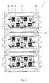
- Fig. 2 shows a top view of the arrangement of three sub-modules (10), according to FIG. 1, to one Power semiconductor module (1) according to the invention.
- the sub-modules (10) are with their Long sides arranged to each other.
- These elongated holes serve as well on the narrow sides of the power semiconductor module remaining recesses (22) of the Fastening the power semiconductor module (1) on a heat sink.
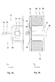
- FIG 3 shows a partial section of a power semiconductor module according to the invention in FIG Top view (a) and side view (b).
- the housing (30) and one of the already described in Fig. 2 elongated holes (24), which is located on the abutting edge (26) forms two sub-modules (10).
- a round hole (72) in the cover (70) covers both sub-modules (10) and is fixed by means of a screw (80) the two sub-modules on a heat sink.
- the cover (70) has one for this Stop surface on which on the through the housing (30) recessed parts (28) of the Base plate (20) rests.
- FIG. 4 shows a further embodiment of a power semiconductor module according to the invention with a snap-lock connection of the lid.
- Submodule (10) arranged housing (30) has a plurality of locking lugs (32). These locking lugs form a snap-locking connection with the associated abutments of the cover (70). This results from the individual assembly of the cover (70)
- Sub-modules (10) a modular power semiconductor module with mutually fixed Sub-modules.
- the cover (70), the locking lugs and the housing (30) have assigned abutments.
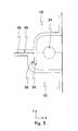
- Fig. 5 shows a detail of a further embodiment of an inventive Power semiconductor module with snap-snap connection of the sub-modules (10).
- They offer Different, also combinable variants of the fixing connection of the Sub modules to each other. It can be the base plate, the housing and / or the cover have such fixing connections.
- An example is a fixing snap-snap connection the housing (30) shown. Each housing points to another Part module facing side at least one, preferably two, locking lugs (34).
- the Latch (34) of one part housing (10) forms with the abutment of the other Part housing (10) a fixing connection. This creates from a plurality of individual Sub-modules the entire power semiconductor module.
- An alternative to connecting individual neighboring sub-modules (10) is to the respective long sides of the power semiconductor module arranged through the housing recessed areas (28, Fig. 3) covering, and for this purpose having stop surfaces, preferably metallic, rail.
- the sub-modules into one Power semiconductor module fixing elements has round holes for screw connections with the heat sink. These round holes are preferably all in flight Recesses (22) and the round or elongated holes (24) formed therefrom Page arranged.
- FIG. 6 shows a top view of a power semiconductor module according to the invention with a Fixing connection of the two sub-modules according to FIG. 5.
- the two round holes (24) and the half-holes (22) are used for fastening (see FIG. 7) on a heat sink.
- This The power module has a cover (not shown) for each sub-module, since here the fixing connection through the snap-snap connection of the housing (30) given is.
- FIG. 7 shows an inventive power semiconductor module (1) with one of the three Sub-modules (10) overlapping cover (70).
- the lid (70) faces its respective Corners extensions (74) that protrude beyond the base plate and down to the heat sink are extended to ensure a secure screw connection through the round holes (72a) of the To ensure cover (70) and the half holes (22, see Fig. 6) with a heat sink.
- auxiliary connections (44) in this embodiment of the power semiconductor module (1) not on the narrow sides of the sub-modules (10) but along their long sides arranged.
Landscapes
- Cooling Or The Like Of Semiconductors Or Solid State Devices (AREA)
- Coupling Device And Connection With Printed Circuit (AREA)
- Inverter Devices (AREA)
- Power Conversion In General (AREA)
- Structures For Mounting Electric Components On Printed Circuit Boards (AREA)
Abstract
Description
- durch die Aufteilung in Teilmodule diese im Fehlerfall einzeln getauscht werden können,
- durch gleichartige Teilmodule eine Fertigung verschiedener Leisungshalbleitermodule mit einem geringeren Teileaufwand durchführbar ist und
- trotz der Ausgestaltung aus einzelnen Teilmodulen das Leistungshalbleitermodul kompatibel zum Stand der Technik, beispielhaft einer 3-Phasen Vollbrückenschaltung, ist.
- Fig. 1
- zeigt ein Teilmodul eines erfindungsgemäßen Leistungshalbleitermoduls in Draufsicht.
- Fig. 2
- zeigt die Anordnung von drei Teilmodulen zu einem erfindungsgemäßen Leistungshalbleitermodul.
- Fig. 3
- zeigt einen Teilausschnitt eines erfindungsgemäßen Leistungshalbleitermoduls in Draufsicht (a) sowie in seitlicher Ansicht (b).
- Fig. 4
- zeigt eine weitere Ausgestaltung eines erfindungsgemäßen Leistungshalbleitermoduls mit einer Schnapp- Rastverbindung des Deckels.
- Fig. 5
- zeigt in einem Ausschnitt eine weitere Ausgestaltung eines erfindungsgemäßen Leistungshalbleitermoduls mit Schnapp- Rastverbindung der Teilmodule.
- Fig. 6
- zeigt ein erfindungsgemäßes Leistungshalbleitermodul mit einer Verbindung der Teilmodule gemäß Fig. 5
- Fig. 7.
- Zeigt ein erfindungsgemäßes Leistungshalbleitermodul mit einem drei Teilmodule überlappenden Deckel.
Claims (7)
- Leistungshalbleitermodul (1) zur Montage auf einem flächigen Körper bestehend aus einer Mehrzahl von Teilmodulen (10), welche ihrerseits aus einer Grundplatte (20) sowie einem rahmenartigen Gehäuse (30) und Anschlusselementen (40) für Last- (42) und Hilfsanschlüsse (44) bestehen, mit mindestens einem innerhalb jedes Gehäuses (30) auf der jeweiligen Grundplatte (20) angeordneten elektrisch isolierenden Substrat (50), das seinerseits besteht aus einem Isolierstoffkörper (52) mit einer Mehrzahl von darauf befindlichen gegeneinander isolierten metallischen Verbindungsbahnen (54), darauf befindlichen und mit diesen Verbindungsbahnen schaltungsgerecht verbundenen Leistungshalbleiterbauelementen (56), wobei
das Leistungshalbleitermodul genau einen, die einzelnen Teilmodule verbindenden und gegeneinander fixierenden Deckel (70) aufweist und / oder alle Teilmodule mittels fixierenden Verbindungen (34,36) zueinander angeordnet sind. - Leistungshalbleitermodul nach Anspruch 1, wobei
der Deckel (70) mit den Teilmodulen (10) mittels Schnapp- Rastverbindungen verbunden ist, wobei die Gehäuse (30) Rastnasen (32) und der Deckel (70) diesen zugeordnete Widerlager aufweist. - Leistungshalbleitermodul nach Anspruch 1, wobei
jedes Teilmodul (10) mindestens zwei rund- oder langlochartige, nicht allseits umschlossene Ausnehmungen (22) aufweist, die sich bei der Anordnung der Teilmodule (10) zu einem Leistungshalbleitermodul (1) an den jeweils aneinander angrenzenden Seiten zu Rund- oder Langlöchern erganzen. - Leistungshalbleitermodul nach Anspruch 2, wobei
der Deckel (70) rundlochartige Ausnehmungen (72) zur Aufnahme von Schrauben (80) aufweist, welche im Stoßbereich (26) der Teilmodule (10) in der Flucht mit den dort Rund- oder Langlöcher (24) bildenden Ausnehmungen (22) angeordnet sind. - Leistungshalbleitermodul nach Anspruch 1, wobei
jedes Teilmodul (10) an einer Grenzseite zu weiteren Teilmodulen mindestens eine Rastnase (34) sowie auf der gegenüberliegenden Grenzseite mindestens ein dieser Rastnase zugeordnetes Widerlager (36) aufweist. - Leistungshalbleitermodul nach Anspruch 5, wobei
die fixierende Verbindung als eine Schnapp- Rastverbindung (34, 36) aller direkt benachbarten Teilmodule ausgebildet ist. - Leistungshalbleitermodul nach Anspruch 2, wobei
die fixierende Verbindung als alle Ausnehmungen (22) sowie die daraus gebildeten Rund- oder Langlöcher (24) der jeweiligen Seite überdeckende Schiene ausgebildet ist.
Applications Claiming Priority (2)
| Application Number | Priority Date | Filing Date | Title |
|---|---|---|---|
| DE10316356 | 2003-04-10 | ||
| DE10316356A DE10316356B4 (de) | 2003-04-10 | 2003-04-10 | Modular aufgebautes Leistungshalbleitermodul |
Publications (2)
| Publication Number | Publication Date |
|---|---|
| EP1467406A1 true EP1467406A1 (de) | 2004-10-13 |
| EP1467406B1 EP1467406B1 (de) | 2007-01-03 |
Family
ID=32864411
Family Applications (1)
| Application Number | Title | Priority Date | Filing Date |
|---|---|---|---|
| EP04006021A Expired - Lifetime EP1467406B1 (de) | 2003-04-10 | 2004-03-13 | Modular aufgebautes Leistungshalbleitermodul |
Country Status (7)
| Country | Link |
|---|---|
| US (1) | US7190070B2 (de) |
| EP (1) | EP1467406B1 (de) |
| JP (1) | JP2004319992A (de) |
| AT (1) | ATE350768T1 (de) |
| DE (2) | DE10316356B4 (de) |
| DK (1) | DK1467406T3 (de) |
| ES (1) | ES2279243T3 (de) |
Cited By (3)
| Publication number | Priority date | Publication date | Assignee | Title |
|---|---|---|---|---|
| EP2003693A3 (de) * | 2007-06-09 | 2010-08-04 | SEMIKRON Elektronik GmbH & Co. KG | Druckkontaktiertes dreiphasiges Stromrichtermodul |
| WO2011006583A1 (de) * | 2009-07-14 | 2011-01-20 | Sew-Eurodrive Gmbh & Co. Kg | Gehäuse |
| DE102017218875C5 (de) * | 2017-10-23 | 2026-03-05 | Semikron Danfoss GmbH | Leistungsmodul-Baugruppe |
Families Citing this family (36)
| Publication number | Priority date | Publication date | Assignee | Title |
|---|---|---|---|---|
| JP4583122B2 (ja) * | 2004-09-28 | 2010-11-17 | 三菱電機株式会社 | 半導体装置及びその製造方法 |
| DE102005037522A1 (de) * | 2005-08-09 | 2007-02-15 | Semikron Elektronik Gmbh & Co. Kg | Leistungshalbleitermodul mit wannenförmigem Grundkörper |
| DE102005039278A1 (de) | 2005-08-19 | 2007-02-22 | Semikron Elektronik Gmbh & Co. Kg | Leistungshalbleitermodul mit Leitungselement |
| DE102005039947B4 (de) | 2005-08-24 | 2011-12-15 | Semikron Elektronik Gmbh & Co. Kg | Leistungshalbleitermodul mit Befestigungseinrichtung |
| DE102007007223B4 (de) | 2007-02-14 | 2008-11-20 | Semikron Elektronik Gmbh & Co. Kg | Modular aufgebautes Leistungshalbleitermodul |
| DE102007016222B3 (de) | 2007-04-04 | 2008-11-06 | Semikron Elektronik Gmbh & Co. Kg | Leistungshalbleitermodul in Druckkontaktausführung sowie Verfahren zur Herstellung desselben |
| DE102007046969B3 (de) * | 2007-09-28 | 2009-04-02 | Siemens Ag | Elektronische Schaltung aus Teilschaltungen und Verfahren zu deren Herstellung und demgemäßer Umrichter oder Schalter |
| US8461623B2 (en) | 2008-07-10 | 2013-06-11 | Mitsubishi Electric Corporation | Power semiconductor module |
| DE102008033410B4 (de) | 2008-07-16 | 2011-06-30 | SEMIKRON Elektronik GmbH & Co. KG, 90431 | Leistungselektronische Verbindungseinrichtung mit einem Leistungshalbleiterbauelement und Herstellungsverfahren hierzu |
| DE102008034148B4 (de) * | 2008-07-22 | 2011-08-25 | Infineon Technologies AG, 85579 | Leistungshalbleitermodulsystem und Verfahren zur Herstellung einer Leistungshalbleiteranordnung |
| US7830681B2 (en) | 2008-09-24 | 2010-11-09 | Teco-Westinghouse Motor Company | Modular multi-pulse transformer rectifier for use in asymmetric multi-level power converter |
| US8279640B2 (en) | 2008-09-24 | 2012-10-02 | Teco-Westinghouse Motor Company | Modular multi-pulse transformer rectifier for use in symmetric multi-level power converter |
| US8237260B2 (en) * | 2008-11-26 | 2012-08-07 | Infineon Technologies Ag | Power semiconductor module with segmented base plate |
| US7940537B2 (en) * | 2008-12-31 | 2011-05-10 | Teco-Westinghouse Motor Company | Partial regeneration in a multi-level power inverter |
| US8223515B2 (en) * | 2009-02-26 | 2012-07-17 | TECO—Westinghouse Motor Company | Pre-charging an inverter using an auxiliary winding |
| US8976526B2 (en) | 2009-06-30 | 2015-03-10 | Teco-Westinghouse Motor Company | Providing a cooling system for a medium voltage drive system |
| US8254076B2 (en) | 2009-06-30 | 2012-08-28 | Teco-Westinghouse Motor Company | Providing modular power conversion |
| US8575479B2 (en) | 2009-06-30 | 2013-11-05 | TECO—Westinghouse Motor Company | Providing a transformer for an inverter |
| US8711530B2 (en) * | 2009-06-30 | 2014-04-29 | Teco-Westinghouse Motor Company | Pluggable power cell for an inverter |
| US8130501B2 (en) | 2009-06-30 | 2012-03-06 | Teco-Westinghouse Motor Company | Pluggable power cell for an inverter |
| JP5602095B2 (ja) | 2011-06-09 | 2014-10-08 | 三菱電機株式会社 | 半導体装置 |
| US8601190B2 (en) | 2011-06-24 | 2013-12-03 | Teco-Westinghouse Motor Company | Providing multiple communication protocols for a control system having a master controller and a slave controller |
| DE102012101666B3 (de) | 2012-02-29 | 2013-05-16 | Infineon Technologies Ag | Leistungshalbleitermodulsystem mit Hinterschneidungsverbindung |
| DE102012206271A1 (de) | 2012-04-17 | 2013-10-17 | Semikron Elektronik Gmbh & Co. Kg | Flüssigkeitsgekühlte Anordnung mit anreihbaren Leistungshalbleitermodulen und mindestens einer Kondensatoreinrichtung und Leistungshalbleitermodul hierzu |
| DE102012206264A1 (de) | 2012-04-17 | 2013-10-17 | Semikron Elektronik Gmbh & Co. Kg | Anreihbares flüssigkeitsgekühltes Leistungshalbleitermodul und Anordnung hiermit |
| US9363930B2 (en) | 2013-03-11 | 2016-06-07 | Teco-Westinghouse Motor Company | Passive two phase cooling solution for low, medium and high voltage drive systems |
| US9153374B2 (en) | 2013-06-28 | 2015-10-06 | Teco-Westinghouse Motor Company | Cooling arrangements for drive systems |
| DE102014115812B4 (de) * | 2014-10-30 | 2019-09-05 | Infineon Technologies Ag | Halbleitermodul und Halbleitermodulanordnung mit geringen Kriechströmen |
| WO2016194048A1 (ja) | 2015-05-29 | 2016-12-08 | 新電元工業株式会社 | 半導体装置、及び、半導体装置の実装方法 |
| CN105374810A (zh) * | 2015-11-23 | 2016-03-02 | 扬州国扬电子有限公司 | 一种功率模块 |
| CN105374803B (zh) * | 2015-11-23 | 2019-02-01 | 扬州国扬电子有限公司 | 一种功率模块 |
| JP2018182119A (ja) * | 2017-04-17 | 2018-11-15 | 三菱電機株式会社 | 半導体装置 |
| DE102020207701A1 (de) | 2020-06-22 | 2021-12-23 | Zf Friedrichshafen Ag | Leistungsmodul zum Betreiben eines Elektrofahrzeugantriebs mit einem Zwischenkreiskondensator |
| EP4068349B1 (de) * | 2021-03-30 | 2023-09-20 | Siemens Aktiengesellschaft | Leistungsmodul |
| USD1078669S1 (en) * | 2023-10-18 | 2025-06-10 | Semikron Danfoss International GmbH | Semiconductor power module for vehicles |
| DE102024105617A1 (de) | 2024-02-28 | 2025-08-28 | Semikron Danfoss GmbH | Leistungselektronische Schalteinrichtung |
Citations (8)
| Publication number | Priority date | Publication date | Assignee | Title |
|---|---|---|---|---|
| US4600968A (en) * | 1984-11-13 | 1986-07-15 | Fuji Electric Co., Ltd. | Semiconductor device package having regions of different thermal properties |
| US5485350A (en) * | 1993-11-26 | 1996-01-16 | Siemens Aktiengesellschaft | Cooled electronic housing |
| EP0828341A2 (de) * | 1996-09-06 | 1998-03-11 | Hitachi, Ltd. | Leistungshalbleiteranordnung in modularer Bauart |
| JP2000156575A (ja) * | 1998-11-20 | 2000-06-06 | Denso Corp | 回路モジュール連結型電子回路装置及びその製造方法 |
| US20020027283A1 (en) * | 1998-05-15 | 2002-03-07 | Kabushiki Kaisha Toshiba | Hermetically sealed semiconductor power module and large scale module comprising the same |
| JP2002184940A (ja) * | 2000-12-18 | 2002-06-28 | Mitsubishi Electric Corp | 電力用半導体装置 |
| US20020153532A1 (en) * | 1997-06-12 | 2002-10-24 | Yukio Sonobe | Power semiconductor module |
| EP1263045A1 (de) * | 2001-06-01 | 2002-12-04 | ABB Schweiz AG | Leistungshalbleitermodul |
Family Cites Families (10)
| Publication number | Priority date | Publication date | Assignee | Title |
|---|---|---|---|---|
| US4790763A (en) * | 1986-04-22 | 1988-12-13 | Amp Incorporated | Programmable modular connector assembly |
| DE3937045A1 (de) | 1989-11-07 | 1991-05-08 | Abb Ixys Semiconductor Gmbh | Leistungshalbleitermodul |
| DE19942770A1 (de) * | 1999-09-08 | 2001-03-15 | Ixys Semiconductor Gmbh | Leistungshalbleiter-Modul |
| EP1128432B1 (de) * | 2000-02-24 | 2016-04-06 | Infineon Technologies AG | Befestigung von Halbleitermodulen an einem Kühlkörper |
| DE10011633A1 (de) | 2000-03-10 | 2001-09-20 | Eupec Gmbh & Co Kg | Anordnung zur Verschaltung von Leistungshalbleiterchips in Modulen |
| DE10024377B4 (de) * | 2000-05-17 | 2006-08-17 | Infineon Technologies Ag | Gehäuseeinrichtung und darin zu verwendendes Kontaktelement |
| DE10024516B4 (de) * | 2000-05-18 | 2006-03-09 | eupec Europäische Gesellschaft für Leistungshalbleiter mbH & Co. KG | Leistungshalbleitermodul |
| JP2002203942A (ja) * | 2000-12-28 | 2002-07-19 | Fuji Electric Co Ltd | パワー半導体モジュール |
| EP1263046A1 (de) * | 2001-06-01 | 2002-12-04 | ABB Schweiz AG | Kontaktanordnung |
| DE10237561C1 (de) * | 2002-08-16 | 2003-10-16 | Semikron Elektronik Gmbh | Induktivitätsarme Schaltungsanordnung bzw. Schaltungsaufbau für Leistungshalbleitermodule |
-
2003
- 2003-04-10 DE DE10316356A patent/DE10316356B4/de not_active Expired - Lifetime
-
2004
- 2004-03-13 ES ES04006021T patent/ES2279243T3/es not_active Expired - Lifetime
- 2004-03-13 DK DK04006021T patent/DK1467406T3/da active
- 2004-03-13 EP EP04006021A patent/EP1467406B1/de not_active Expired - Lifetime
- 2004-03-13 DE DE502004002495T patent/DE502004002495D1/de not_active Expired - Lifetime
- 2004-03-13 AT AT04006021T patent/ATE350768T1/de active
- 2004-03-29 JP JP2004095430A patent/JP2004319992A/ja active Pending
- 2004-04-09 US US10/821,308 patent/US7190070B2/en not_active Expired - Lifetime
Patent Citations (8)
| Publication number | Priority date | Publication date | Assignee | Title |
|---|---|---|---|---|
| US4600968A (en) * | 1984-11-13 | 1986-07-15 | Fuji Electric Co., Ltd. | Semiconductor device package having regions of different thermal properties |
| US5485350A (en) * | 1993-11-26 | 1996-01-16 | Siemens Aktiengesellschaft | Cooled electronic housing |
| EP0828341A2 (de) * | 1996-09-06 | 1998-03-11 | Hitachi, Ltd. | Leistungshalbleiteranordnung in modularer Bauart |
| US20020153532A1 (en) * | 1997-06-12 | 2002-10-24 | Yukio Sonobe | Power semiconductor module |
| US20020027283A1 (en) * | 1998-05-15 | 2002-03-07 | Kabushiki Kaisha Toshiba | Hermetically sealed semiconductor power module and large scale module comprising the same |
| JP2000156575A (ja) * | 1998-11-20 | 2000-06-06 | Denso Corp | 回路モジュール連結型電子回路装置及びその製造方法 |
| JP2002184940A (ja) * | 2000-12-18 | 2002-06-28 | Mitsubishi Electric Corp | 電力用半導体装置 |
| EP1263045A1 (de) * | 2001-06-01 | 2002-12-04 | ABB Schweiz AG | Leistungshalbleitermodul |
Non-Patent Citations (2)
| Title |
|---|
| PATENT ABSTRACTS OF JAPAN vol. 2000, no. 09 13 October 2000 (2000-10-13) * |
| PATENT ABSTRACTS OF JAPAN vol. 2002, no. 10 10 October 2002 (2002-10-10) * |
Cited By (3)
| Publication number | Priority date | Publication date | Assignee | Title |
|---|---|---|---|---|
| EP2003693A3 (de) * | 2007-06-09 | 2010-08-04 | SEMIKRON Elektronik GmbH & Co. KG | Druckkontaktiertes dreiphasiges Stromrichtermodul |
| WO2011006583A1 (de) * | 2009-07-14 | 2011-01-20 | Sew-Eurodrive Gmbh & Co. Kg | Gehäuse |
| DE102017218875C5 (de) * | 2017-10-23 | 2026-03-05 | Semikron Danfoss GmbH | Leistungsmodul-Baugruppe |
Also Published As
| Publication number | Publication date |
|---|---|
| DE502004002495D1 (de) | 2007-02-15 |
| DE10316356A1 (de) | 2004-11-11 |
| US20050093122A9 (en) | 2005-05-05 |
| ES2279243T3 (es) | 2007-08-16 |
| US7190070B2 (en) | 2007-03-13 |
| US20050012190A1 (en) | 2005-01-20 |
| DE10316356B4 (de) | 2012-07-26 |
| DK1467406T3 (da) | 2007-05-14 |
| EP1467406B1 (de) | 2007-01-03 |
| JP2004319992A (ja) | 2004-11-11 |
| ATE350768T1 (de) | 2007-01-15 |
Similar Documents
| Publication | Publication Date | Title |
|---|---|---|
| DE10316356B4 (de) | Modular aufgebautes Leistungshalbleitermodul | |
| DE10237561C1 (de) | Induktivitätsarme Schaltungsanordnung bzw. Schaltungsaufbau für Leistungshalbleitermodule | |
| DE102009002993B4 (de) | Leistungshalbleitermodul mit beabstandeten Schaltungsträgern | |
| DE102011083223B4 (de) | Leistungshalbleitermodul mit integrierter Dickschichtleiterplatte | |
| DE102010002627B4 (de) | Niederinduktive Leistungshalbleiterbaugruppen | |
| WO2019158390A1 (de) | Leistungselektronikanordnung | |
| DE102011078811B3 (de) | Leistungselektronisches System mit einer Kühleinrichtung | |
| DE10296619B4 (de) | Leistungsmodul | |
| DE19826731C2 (de) | Halbbrückenbaugruppe | |
| DE102021110251B4 (de) | Leistungshalbleiteranordnung und Wechselrichterbrücke mit Leistungshalbleiteranordnung | |
| DE112017006619B4 (de) | Schaltungsanordnung und elektrischer Verteilerkasten | |
| EP3404818B1 (de) | Halbleiterschaltanordnung | |
| DE102019103032B4 (de) | Schaltnetzteilvorrichtung | |
| DE102007046969B3 (de) | Elektronische Schaltung aus Teilschaltungen und Verfahren zu deren Herstellung und demgemäßer Umrichter oder Schalter | |
| DE10337640A1 (de) | Leistungshalbleitermodul mit verbessertem thermischen Kontakt | |
| DE102022113638A1 (de) | Leiterplattenanordnung | |
| EP1501125A2 (de) | Leistungshalbleitermodul mit skalierbarer Aufbautechnik | |
| EP1433204B1 (de) | Anordnung mit leistungshalbleiterbauelementen zur leistungssteuerung hoher ströme und anwendung der anordnung | |
| DE102011078806B4 (de) | Herstellungsverfahren für ein leistungselektronisches System mit einer Kühleinrichtung | |
| DE102020205109A1 (de) | Elektrische Schaltungsanordnung für einen Leistungswandler | |
| DE10249205B3 (de) | Leistungsbauelementanordnung zur mechatronischen Integration von Leistungsbauelementen | |
| DE19646396C2 (de) | Leistungshalbleitermodul für verschiedene Schaltungsvarianten | |
| DE102017106515B4 (de) | 3-Pegel-Leistungsmodul | |
| EP3799536A1 (de) | Träger für elektrische bauelemente und elektronikmodul | |
| DE102005039947B4 (de) | Leistungshalbleitermodul mit Befestigungseinrichtung |
Legal Events
| Date | Code | Title | Description |
|---|---|---|---|
| PUAI | Public reference made under article 153(3) epc to a published international application that has entered the european phase |
Free format text: ORIGINAL CODE: 0009012 |
|
| 17P | Request for examination filed |
Effective date: 20040811 |
|
| AK | Designated contracting states |
Kind code of ref document: A1 Designated state(s): AT BE BG CH CY CZ DE DK EE ES FI FR GB GR HU IE IT LI LU MC NL PL PT RO SE SI SK TR |
|
| AX | Request for extension of the european patent |
Extension state: AL LT LV MK |
|
| AKX | Designation fees paid |
Designated state(s): AT BE BG CH CY CZ DE DK EE ES FI FR GB GR HU IE IT LI LU MC NL PL PT RO SE SI SK TR |
|
| RAP1 | Party data changed (applicant data changed or rights of an application transferred) |
Owner name: SEMIKRON ELEKTRONIK GMBH & CO. KG |
|
| GRAP | Despatch of communication of intention to grant a patent |
Free format text: ORIGINAL CODE: EPIDOSNIGR1 |
|
| GRAS | Grant fee paid |
Free format text: ORIGINAL CODE: EPIDOSNIGR3 |
|
| GRAA | (expected) grant |
Free format text: ORIGINAL CODE: 0009210 |
|
| AK | Designated contracting states |
Kind code of ref document: B1 Designated state(s): AT BE BG CH CY CZ DE DK EE ES FI FR GB GR HU IE IT LI LU MC NL PL PT RO SE SI SK TR |
|
| PG25 | Lapsed in a contracting state [announced via postgrant information from national office to epo] |
Ref country code: PL Free format text: LAPSE BECAUSE OF FAILURE TO SUBMIT A TRANSLATION OF THE DESCRIPTION OR TO PAY THE FEE WITHIN THE PRESCRIBED TIME-LIMIT Effective date: 20070103 Ref country code: FI Free format text: LAPSE BECAUSE OF FAILURE TO SUBMIT A TRANSLATION OF THE DESCRIPTION OR TO PAY THE FEE WITHIN THE PRESCRIBED TIME-LIMIT Effective date: 20070103 Ref country code: IE Free format text: LAPSE BECAUSE OF FAILURE TO SUBMIT A TRANSLATION OF THE DESCRIPTION OR TO PAY THE FEE WITHIN THE PRESCRIBED TIME-LIMIT Effective date: 20070103 Ref country code: SI Free format text: LAPSE BECAUSE OF FAILURE TO SUBMIT A TRANSLATION OF THE DESCRIPTION OR TO PAY THE FEE WITHIN THE PRESCRIBED TIME-LIMIT Effective date: 20070103 |
|
| REG | Reference to a national code |
Ref country code: GB Ref legal event code: FG4D Free format text: NOT ENGLISH |
|
| REF | Corresponds to: |
Ref document number: 502004002495 Country of ref document: DE Date of ref document: 20070215 Kind code of ref document: P |
|
| REG | Reference to a national code |
Ref country code: IE Ref legal event code: FG4D Free format text: LANGUAGE OF EP DOCUMENT: GERMAN |
|
| PG25 | Lapsed in a contracting state [announced via postgrant information from national office to epo] |
Ref country code: BG Free format text: LAPSE BECAUSE OF FAILURE TO SUBMIT A TRANSLATION OF THE DESCRIPTION OR TO PAY THE FEE WITHIN THE PRESCRIBED TIME-LIMIT Effective date: 20070404 |
|
| GBT | Gb: translation of ep patent filed (gb section 77(6)(a)/1977) |
Effective date: 20070315 |
|
| REG | Reference to a national code |
Ref country code: DK Ref legal event code: T3 |
|
| PG25 | Lapsed in a contracting state [announced via postgrant information from national office to epo] |
Ref country code: PT Free format text: LAPSE BECAUSE OF FAILURE TO SUBMIT A TRANSLATION OF THE DESCRIPTION OR TO PAY THE FEE WITHIN THE PRESCRIBED TIME-LIMIT Effective date: 20070604 |
|
| REG | Reference to a national code |
Ref country code: SE Ref legal event code: TRGR |
|
| ET | Fr: translation filed | ||
| REG | Reference to a national code |
Ref country code: ES Ref legal event code: FG2A Ref document number: 2279243 Country of ref document: ES Kind code of ref document: T3 |
|
| REG | Reference to a national code |
Ref country code: IE Ref legal event code: FD4D |
|
| REG | Reference to a national code |
Ref country code: CH Ref legal event code: NV Representative=s name: BRAUNPAT BRAUN EDER AG |
|
| PLBE | No opposition filed within time limit |
Free format text: ORIGINAL CODE: 0009261 |
|
| STAA | Information on the status of an ep patent application or granted ep patent |
Free format text: STATUS: NO OPPOSITION FILED WITHIN TIME LIMIT |
|
| 26N | No opposition filed |
Effective date: 20071005 |
|
| BERE | Be: lapsed |
Owner name: SEMIKRON ELEKTRONIK G.M.B.H. & CO. KG Effective date: 20070331 |
|
| PG25 | Lapsed in a contracting state [announced via postgrant information from national office to epo] |
Ref country code: BE Free format text: LAPSE BECAUSE OF NON-PAYMENT OF DUE FEES Effective date: 20070331 Ref country code: RO Free format text: LAPSE BECAUSE OF FAILURE TO SUBMIT A TRANSLATION OF THE DESCRIPTION OR TO PAY THE FEE WITHIN THE PRESCRIBED TIME-LIMIT Effective date: 20070103 Ref country code: CZ Free format text: LAPSE BECAUSE OF FAILURE TO SUBMIT A TRANSLATION OF THE DESCRIPTION OR TO PAY THE FEE WITHIN THE PRESCRIBED TIME-LIMIT Effective date: 20070103 |
|
| PG25 | Lapsed in a contracting state [announced via postgrant information from national office to epo] |
Ref country code: MC Free format text: LAPSE BECAUSE OF NON-PAYMENT OF DUE FEES Effective date: 20070331 |
|
| PG25 | Lapsed in a contracting state [announced via postgrant information from national office to epo] |
Ref country code: GR Free format text: LAPSE BECAUSE OF FAILURE TO SUBMIT A TRANSLATION OF THE DESCRIPTION OR TO PAY THE FEE WITHIN THE PRESCRIBED TIME-LIMIT Effective date: 20070404 |
|
| PG25 | Lapsed in a contracting state [announced via postgrant information from national office to epo] |
Ref country code: EE Free format text: LAPSE BECAUSE OF FAILURE TO SUBMIT A TRANSLATION OF THE DESCRIPTION OR TO PAY THE FEE WITHIN THE PRESCRIBED TIME-LIMIT Effective date: 20070103 |
|
| PG25 | Lapsed in a contracting state [announced via postgrant information from national office to epo] |
Ref country code: CY Free format text: LAPSE BECAUSE OF FAILURE TO SUBMIT A TRANSLATION OF THE DESCRIPTION OR TO PAY THE FEE WITHIN THE PRESCRIBED TIME-LIMIT Effective date: 20070103 |
|
| PG25 | Lapsed in a contracting state [announced via postgrant information from national office to epo] |
Ref country code: LU Free format text: LAPSE BECAUSE OF NON-PAYMENT OF DUE FEES Effective date: 20070313 |
|
| PG25 | Lapsed in a contracting state [announced via postgrant information from national office to epo] |
Ref country code: HU Free format text: LAPSE BECAUSE OF FAILURE TO SUBMIT A TRANSLATION OF THE DESCRIPTION OR TO PAY THE FEE WITHIN THE PRESCRIBED TIME-LIMIT Effective date: 20070704 Ref country code: TR Free format text: LAPSE BECAUSE OF FAILURE TO SUBMIT A TRANSLATION OF THE DESCRIPTION OR TO PAY THE FEE WITHIN THE PRESCRIBED TIME-LIMIT Effective date: 20070103 |
|
| REG | Reference to a national code |
Ref country code: FR Ref legal event code: PLFP Year of fee payment: 13 |
|
| REG | Reference to a national code |
Ref country code: FR Ref legal event code: PLFP Year of fee payment: 14 |
|
| PGFP | Annual fee paid to national office [announced via postgrant information from national office to epo] |
Ref country code: SE Payment date: 20170327 Year of fee payment: 14 Ref country code: NL Payment date: 20170323 Year of fee payment: 14 |
|
| PGFP | Annual fee paid to national office [announced via postgrant information from national office to epo] |
Ref country code: AT Payment date: 20170322 Year of fee payment: 14 Ref country code: DK Payment date: 20170327 Year of fee payment: 14 Ref country code: SK Payment date: 20170303 Year of fee payment: 14 |
|
| REG | Reference to a national code |
Ref country code: FR Ref legal event code: PLFP Year of fee payment: 15 |
|
| REG | Reference to a national code |
Ref country code: CH Ref legal event code: PCAR Free format text: NEW ADDRESS: HOLEESTRASSE 87, 4054 BASEL (CH) |
|
| REG | Reference to a national code |
Ref country code: DK Ref legal event code: EBP Effective date: 20180331 |
|
| PG25 | Lapsed in a contracting state [announced via postgrant information from national office to epo] |
Ref country code: SE Free format text: LAPSE BECAUSE OF NON-PAYMENT OF DUE FEES Effective date: 20180314 |
|
| REG | Reference to a national code |
Ref country code: NL Ref legal event code: MM Effective date: 20180401 |
|
| REG | Reference to a national code |
Ref country code: AT Ref legal event code: MM01 Ref document number: 350768 Country of ref document: AT Kind code of ref document: T Effective date: 20180313 |
|
| REG | Reference to a national code |
Ref country code: SK Ref legal event code: MM4A Ref document number: E 1754 Country of ref document: SK Effective date: 20180313 |
|
| PG25 | Lapsed in a contracting state [announced via postgrant information from national office to epo] |
Ref country code: NL Free format text: LAPSE BECAUSE OF NON-PAYMENT OF DUE FEES Effective date: 20180401 |
|
| PG25 | Lapsed in a contracting state [announced via postgrant information from national office to epo] |
Ref country code: SK Free format text: LAPSE BECAUSE OF NON-PAYMENT OF DUE FEES Effective date: 20180313 Ref country code: AT Free format text: LAPSE BECAUSE OF NON-PAYMENT OF DUE FEES Effective date: 20180313 |
|
| PG25 | Lapsed in a contracting state [announced via postgrant information from national office to epo] |
Ref country code: DK Free format text: LAPSE BECAUSE OF NON-PAYMENT OF DUE FEES Effective date: 20180331 |
|
| PGFP | Annual fee paid to national office [announced via postgrant information from national office to epo] |
Ref country code: FR Payment date: 20230320 Year of fee payment: 20 |
|
| PGFP | Annual fee paid to national office [announced via postgrant information from national office to epo] |
Ref country code: GB Payment date: 20230323 Year of fee payment: 20 Ref country code: DE Payment date: 20230331 Year of fee payment: 20 |
|
| PGFP | Annual fee paid to national office [announced via postgrant information from national office to epo] |
Ref country code: CH Payment date: 20230402 Year of fee payment: 20 Ref country code: IT Payment date: 20230331 Year of fee payment: 20 Ref country code: ES Payment date: 20230414 Year of fee payment: 20 |
|
| REG | Reference to a national code |
Ref country code: DE Ref legal event code: R071 Ref document number: 502004002495 Country of ref document: DE |
|
| REG | Reference to a national code |
Ref country code: CH Ref legal event code: PL |
|
| REG | Reference to a national code |
Ref country code: ES Ref legal event code: FD2A Effective date: 20240327 |
|
| REG | Reference to a national code |
Ref country code: GB Ref legal event code: PE20 Expiry date: 20240312 |
|
| PG25 | Lapsed in a contracting state [announced via postgrant information from national office to epo] |
Ref country code: ES Free format text: LAPSE BECAUSE OF EXPIRATION OF PROTECTION Effective date: 20240314 |
|
| PG25 | Lapsed in a contracting state [announced via postgrant information from national office to epo] |
Ref country code: ES Free format text: LAPSE BECAUSE OF EXPIRATION OF PROTECTION Effective date: 20240314 Ref country code: GB Free format text: LAPSE BECAUSE OF EXPIRATION OF PROTECTION Effective date: 20240312 |
|
| REG | Reference to a national code |
Ref country code: DE Ref legal event code: R081 Ref document number: 502004002495 Country of ref document: DE Owner name: SEMIKRON DANFOSS ELEKTRONIK GMBH & CO. KG, DE Free format text: FORMER OWNER: SEMIKRON ELEKTRONIK GMBH & CO. KG, 90431 NUERNBERG, DE |