EP1467480B1 - Fernsehtuner - Google Patents
Fernsehtuner Download PDFInfo
- Publication number
- EP1467480B1 EP1467480B1 EP04003902A EP04003902A EP1467480B1 EP 1467480 B1 EP1467480 B1 EP 1467480B1 EP 04003902 A EP04003902 A EP 04003902A EP 04003902 A EP04003902 A EP 04003902A EP 1467480 B1 EP1467480 B1 EP 1467480B1
- Authority
- EP
- European Patent Office
- Prior art keywords
- circuit
- terminal
- television
- inductor
- television signal
- Prior art date
- Legal status (The legal status is an assumption and is not a legal conclusion. Google has not performed a legal analysis and makes no representation as to the accuracy of the status listed.)
- Expired - Lifetime
Links
- 239000003990 capacitor Substances 0.000 claims description 23
- 238000010586 diagram Methods 0.000 description 5
- 230000010355 oscillation Effects 0.000 description 3
- 229920006395 saturated elastomer Polymers 0.000 description 3
- 238000013459 approach Methods 0.000 description 2
- 238000006243 chemical reaction Methods 0.000 description 2
- 230000008878 coupling Effects 0.000 description 1
- 238000010168 coupling process Methods 0.000 description 1
- 238000005859 coupling reaction Methods 0.000 description 1
- 230000001419 dependent effect Effects 0.000 description 1
Images

Classifications
-
- H—ELECTRICITY
- H03—ELECTRONIC CIRCUITRY
- H03D—DEMODULATION OR TRANSFERENCE OF MODULATION FROM ONE CARRIER TO ANOTHER
- H03D7/00—Transference of modulation from one carrier to another, e.g. frequency-changing
- H03D7/14—Balanced arrangements
- H03D7/1425—Balanced arrangements with transistors
-
- H—ELECTRICITY
- H03—ELECTRONIC CIRCUITRY
- H03D—DEMODULATION OR TRANSFERENCE OF MODULATION FROM ONE CARRIER TO ANOTHER
- H03D7/00—Transference of modulation from one carrier to another, e.g. frequency-changing
- H03D7/14—Balanced arrangements
- H03D7/1425—Balanced arrangements with transistors
- H03D7/1433—Balanced arrangements with transistors using bipolar transistors
-
- H—ELECTRICITY
- H03—ELECTRONIC CIRCUITRY
- H03D—DEMODULATION OR TRANSFERENCE OF MODULATION FROM ONE CARRIER TO ANOTHER
- H03D7/00—Transference of modulation from one carrier to another, e.g. frequency-changing
- H03D7/14—Balanced arrangements
- H03D7/1425—Balanced arrangements with transistors
- H03D7/1458—Double balanced arrangements, i.e. where both input signals are differential
-
- H—ELECTRICITY
- H04—ELECTRIC COMMUNICATION TECHNIQUE
- H04N—PICTORIAL COMMUNICATION, e.g. TELEVISION
- H04N5/00—Details of television systems
- H04N5/44—Receiver circuitry for the reception of television signals according to analogue transmission standards
- H04N5/50—Tuning indicators; Automatic tuning control
-
- H—ELECTRICITY
- H03—ELECTRONIC CIRCUITRY
- H03D—DEMODULATION OR TRANSFERENCE OF MODULATION FROM ONE CARRIER TO ANOTHER
- H03D2200/00—Indexing scheme relating to details of demodulation or transference of modulation from one carrier to another covered by H03D
- H03D2200/0001—Circuit elements of demodulators
- H03D2200/0023—Balun circuits
-
- H—ELECTRICITY
- H03—ELECTRONIC CIRCUITRY
- H03D—DEMODULATION OR TRANSFERENCE OF MODULATION FROM ONE CARRIER TO ANOTHER
- H03D2200/00—Indexing scheme relating to details of demodulation or transference of modulation from one carrier to another covered by H03D
- H03D2200/0001—Circuit elements of demodulators
- H03D2200/0025—Gain control circuits
Definitions
- the present invention relates to a television tuner according to the preamble of claim 1.
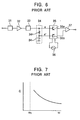
- Fig. 6 shows the configuration of a conventional television tuner of the above type.
- an input tuning circuit 31 can be tuned to, for example, a television signal in a desired channel among the channels of the UHF band.
- the tuned television signal is amplified by a radio-frequency amplifier 32.
- the amplified signal is further selected by an interstage tuning circuit 33.
- the interstage tuning circuit 33 thus outputs an unbalanced signal, which is input to a balun circuit 34.
- the balun circuit 34 is implemented by a series resonance circuit including a capacitor 34a and an inductor 34b. One end of the capacitor 34a is grounded.
- the inductor 34b is connected in series with the capacitor 34a, and one end of the inductor 34b receives input of an unbalanced television signal e.
- the series resonance circuit is arranged such that the resonant frequency thereof is not higher than a lowest frequency of television signals.
- a television signal e' that appears at a node between the capacitor 34a and the inductor 34b has an opposite phase with respect to the television signal e that is input to the inductor 34b. Accordingly, balanced television signals (e, e') are output from the balun circuit 34.
- the balanced television signals are input to two transistors 35a and 35b of a mixer circuit 35, the transistors 35a and 35b being differentially connected to each other.
- the mixer circuit 35 is of the type generally referred to as Gilbert mixer circuit.
- the television signals input to the mixer circuit 35 are mixed with local oscillation signals supplied from an oscillator 36, and are thereby converted into intermediate-frequency signals.
- the balanced intermediate-frequency signals output from the mixer circuit 35 are input to an intermediate-frequency amplifier 37 via a balanced intermediate-frequency tuning circuit (not shown), where the signals are amplified.
- the present invention provides a television tuner including the features of claim 1.
- Preferred embodiments are defined by the dependent claims. Accordingly, increase in gain at lower frequencies of a reception band is suppressed, serving to achieve a flat gain.
- the mixer circuit is implemented by an integrated circuit and the resisting device is formed within the integrated circuit. Accordingly, increase in cost due to addition of the resisting device is avoided.
- a radio-frequency amplifier for amplifying the television signal is provided before the tuning circuit, and the resisting device is activated when power is supplied to the radio-frequency amplifier to allow operation of the radio-frequency amplifier. Accordingly, when a television signal is received, balanced television signals are input to the mixer circuit.
- the resisting device may be implemented by a switching transistor, one of the collector and the emitter of the switching transistor being connected to the second input terminal of the mixer circuit and the other of the collector and the emitter being DC-connected to a power-supply terminal of the radio-frequency amplifier, with a power-supply voltage applied to one of the collector and the emitter of the switching transistor to turn the switching transistor on or off. Accordingly, power is supplied to the radio-frequency amplifier via the switching transistor that has been turned on, and the ON resistance (saturated resistance) of the switching transistor acts as a resistive component, allowing balanced television signals to be input to the mixer circuit.
- the integrated circuit has a first terminal coupled to the first input terminal of the mixer circuit and a second terminal coupled to the second input terminal of the mixer circuit, the one end of the inductor is connected to the first terminal and the node between the inductor and the capacitor is connected to the second terminal, and the power-supply terminal of the radio-frequency amplifier is DC-connected to the second terminal. Accordingly, power supply to the radio-frequency amplifier is simplified.
- Fig. 1 shows the basic configuration of a television tuner according to the present invention.
- an input tuning circuit 1 can be tuned to, for example, a television signal in a desired channel among the channels of the UHF band.
- the tuned television signal is amplified by a radio-frequency amplifier 2.
- the amplified signal is further selected by an interstage tuning circuit 3.
- the interstage tuning circuit 3 thus outputs an unbalanced television signal, which is input to a balun circuit 4.
- the balun circuit 4 is implemented by a series resonance circuit including a capacitor 4a and an inductor 4b. One end of the capacitor 4a is grounded.
- the inductor 4b is connected in series with the capacitor 4a, and one end of the inductor 4b receives input of an unbalanced television signal e.
- the series resonance circuit is arranged such that the resonant frequency thereof is not higher than a lowest frequency of television signals.
- a television signal e' that appears at a node between the capacitor 4a and the inductor 4b has an opposite phase with respect to the television signal e that is input to the inductor 4b. Accordingly, balanced television signals (e and e') are output from the balun circuit 4.
- the balanced television signals are input to a balanced mixer circuit 5 of the type generally referred to as Gilbert mixer.
- the mixer circuit 5 includes transistors 5a and 5b that are differentially connected to each other.
- One of the television signals namely, the television signal e output from the interstage tuning circuit 3, is input directly to one 5a of the two transistors 5a and 5b.
- the other television signal namely, the television signal e' that appears at the node between the capacitor 4a and the inductor 4b, is input to the other transistor 5b via a resisting device 6, for example, a resistor.
- the television signals input to the mixer circuit 5 are mixed with balanced local oscillation signals that are supplied from an oscillator 7, and are thereby converted into intermediate-frequency signals.
- the balanced intermediate-frequency signals output from the mixer circuit 5 are input to an intermediate-frequency amplifier 8 via a balanced intermediate-frequency tuning circuit (not shown), where the signals are amplified.
- Fig. 2 shows a specific configuration according to a first embodiment of the present invention.
- the mixer circuit 5 is included in an integrated circuit 10 having a first terminal 10a and a second terminal 10b.
- the two transistors 5a and 5b are differentially connected to each other by a coupling resistor 5c connected between the emitters the transistors 5a and 5b and by constant current sources 5d and 5e connected to the respective emitters of the transistors 5a and 5b.
- transistors that are differentially connected to each other are connected to the respective collectors of the transistors 5a and 5b, and local oscillation signals are supplied to the respective bases of the transistors from the oscillator 7.
- the base of the transistor 5a which serves as an input terminal, is coupled to the first terminal 10a.
- the resisting device 6 is coupled between the base of the transistor 5b, which serves as another input terminal, and the second terminal 10b. Obviously, the resisting device 6 is formed within the integrated circuit 10.
- the balun circuit 4 is provided externally to the integrated circuit 10.
- the inductor 4b is connected between the first terminal 10a and the second terminal 10b.
- the capacitor 4a is connected between the second terminal 10b and the ground.
- a television signal output from the interstage tuning circuit 3 be denoted as e
- the capacitance of the capacitor 4a in the balun circuit 4 as C 1
- the inductance of the inductor 4b as L
- the resistance of the resisting device 6 R
- the value of internal capacitance 5f of the transistor 5b as C 2
- a television signal input to the base of the transistor 5b as e''.
- equation (2) includes an imaginary part, the television signal e'' input to the transistor 5b is not exactly in opposite phase with the television signal e output from the interstage tuning circuit 3. However, these signals have substantially opposite phases when ⁇ C 2 R is chosen to be sufficiently smaller than 1. Actually, R is on the order of 30 to 70 ⁇ , and C 2 is on the order of 2 pF. Thus, ⁇ C 2 R is smaller than 1. Furthermore, in this case, it is required that ( ⁇ 2 LC 1 - 1) be greater than 0.
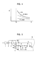
- Fig. 4 schematically shows the variation in the absolute value E" in relation to the resistance of the resisting device 6.
- An appropriate value for the actual resistance of the resisting device 6 is on the order of 30 to 70 ⁇ .
- Fig. 5 shows a specific configuration according to a second embodiment of the present invention.
- an NPN (or PNP) switching transistor is used as the resisting device 6.
- the emitter of the switching transistor is connected to the second terminal 10b, and the collector of the switching transistor is coupled to the base of the transistor 5b in the mixer circuit 5.
- the collector of the switching transistor receives a power-supply voltage via a feed resistor 9.
- the switching transistor is turned on or off according to a switching signal input to the base thereof.
- a power-supply terminal of the radio-frequency amplifier 2 is DC-connected to the second terminal 10b.
- the switching transistor when the switching transistor is turned on, power is supplied to the radio-frequency amplifier 2 via the emitter of the switching transistor. Since the saturated resistance of the switching transistor that has been turned on is several tens ohm, the switching transistor functions as the resisting device 6. That is, when a television signal in the UHF band is to be received, the switching transistor is turned on, whereby the radio-frequency amplifier 2 is activated, and balanced television signals are input to the mixer circuit 5 due to the saturated resistance of the switching transistor.
- the switching transistor When a television signal in the UHF band is not to be received, for example, when a television signal in the VHF band is to be received by a VHF tuner unit that is not shown, the switching transistor is turned off, whereby input of a television signal to the mixer circuit 5 is stopped.
- the switching transistor When the switching transistor is implemented by a PNP transistor, the collector thereof is connected to the second terminal 10b, the emitter thereof is coupled to the base of the transistor 5b of the mixer circuit 5, and the emitter thereof receives a power-supply voltage.
Landscapes
- Engineering & Computer Science (AREA)
- Power Engineering (AREA)
- Multimedia (AREA)
- Signal Processing (AREA)
- Superheterodyne Receivers (AREA)
- Input Circuits Of Receivers And Coupling Of Receivers And Audio Equipment (AREA)
Claims (5)
- Fernsehtuner, aufweisend:eine Abstimmschaltung (3) zur Abstimmung auf ein Fernsehsignal in einem erwünschten Kanal unter Kanälen innerhalb eines vorherbestimmten Bandes;eine symmetrische Mischerschaltung (5) für die Umwandlung des Fernsehsignals in ein Zwischenfrequenzsignal; undeine Symmetrierschaltung (4), die zwischen der Abstimmschaltung (3) und der Mischerschaltung (5) angeordnet ist;wobei die Symmetrierschaltung (4) einen Kondensator (4a) und eine Spule (4b) umfasst, ein Ende des Kondensators (4a) masseverbunden ist und die Spule (4b) mit dem Kondensator (4a) in Serie geschaltet ist und eines seiner Enden mit einem ersten Eingangsanschluss (10a) der Mischerschaltung (5) verbunden ist und wobei eine Ausgabe eines unsymmetrischen Fernsehsignals von der Abstimmschaltung (3) dem ersten Eingangsanschluss (10a) zugeführt wird, dadurch gekennzeichnet, dass ein Fernsehsignal, das an einem Knotenpunkt zwischen der Spule (4b) und dem Kondensator (4a) erscheint, über eine Widerstandseinrichtung (6) einem zweiten Eingangsanschluss (10b) der Mischerschaltung (5) zugeführt wird, so dass die Verstärkungsveränderung des Tuners (3) bezüglich der von der Symmetrierschaltung (4) bewirkten Frequenz reduziert wird, um dabei eine flache Verstärkung über das gesamte Empfangsband zu erreichen.
- Fernsehtuner nach Anspruch 1, wobei die Mischerschaltung (5) durch eine integrierte Schaltung realisiert ist und die Widerstandseinrichtung (6) innerhalb der integrierten Schaltung gebildet ist.
- Fernsehtuner nach Anspruch 1 oder 2, wobei ein Hochfrequenzverstärker (2) zur Verstärkung des Fernsehsignals vor der Abstimmschaltung (3) vorgesehen ist und wobei die Widerstandseinrichtung (6) aktiviert wird, wenn dem Hochfrequenzverstärker (2) Energie zugeführt wird, um den Betrieb des Hochfrequenzverstärkers (2) zu erlauben.
- Fernsehtuner nach Anspruch 3, wobei die Widerstandseinrichtung (6) durch einen Schalttransistor realisiert ist, einer von dem Kollektor und dem Emitter des Schalttransistors mit dem zweiten Eingangsanschluss (10b) der Mischerschaltung (5) verbunden ist und der andere von dem Kollektor und dem Emitter gleichstrommäßig mit einem Energieversorgungsanschluss des Hochfrequenzverstärkers (2) verbunden ist und wobei eine Energieversorgungsspannung an einen von dem Kollektor und dem Emitter des Schalttransistors angelegt wird, um den Schalttransistor ein- oder auszuschalten.
- Fernsehtuner nach Anspruch 4, wobei die integrierte Schaltung einen ersten Anschluss hat, der mit dem ersten Eingangsanschluss (10a) der Mischerschaltung (5) gekoppelt ist, und einen zweiten Anschluss, der mit dem zweiten Eingangsanschluss (10b) der Mischerschaltung (5) gekoppelt ist, wobei das eine Ende der Spule (4b) mit dem ersten Anschluss verbunden ist und der Knotenpunkt zwischen der Spule (4b) und dem Kondensator (4a) mit dem zweiten Anschluss verbunden ist und wobei der Energieversorgungsanschluss des Hochfrequenzverstärkers (2) gleichstrommäßig mit dem zweiten Anschluss verbunden ist.
Applications Claiming Priority (2)
| Application Number | Priority Date | Filing Date | Title |
|---|---|---|---|
| JP2003000960U | 2003-02-27 | ||
| JP2003000960U JP3096169U (ja) | 2003-02-27 | 2003-02-27 | テレビジョンチューナ |
Publications (3)
| Publication Number | Publication Date |
|---|---|
| EP1467480A2 EP1467480A2 (de) | 2004-10-13 |
| EP1467480A3 EP1467480A3 (de) | 2005-02-16 |
| EP1467480B1 true EP1467480B1 (de) | 2006-10-04 |
Family
ID=32866171
Family Applications (1)
| Application Number | Title | Priority Date | Filing Date |
|---|---|---|---|
| EP04003902A Expired - Lifetime EP1467480B1 (de) | 2003-02-27 | 2004-02-20 | Fernsehtuner |
Country Status (3)
| Country | Link |
|---|---|
| EP (1) | EP1467480B1 (de) |
| JP (1) | JP3096169U (de) |
| DE (1) | DE602004002609T2 (de) |
-
2003
- 2003-02-27 JP JP2003000960U patent/JP3096169U/ja not_active Expired - Lifetime
-
2004
- 2004-02-20 DE DE602004002609T patent/DE602004002609T2/de not_active Expired - Lifetime
- 2004-02-20 EP EP04003902A patent/EP1467480B1/de not_active Expired - Lifetime
Also Published As
| Publication number | Publication date |
|---|---|
| EP1467480A3 (de) | 2005-02-16 |
| JP3096169U (ja) | 2003-09-05 |
| EP1467480A2 (de) | 2004-10-13 |
| DE602004002609D1 (de) | 2006-11-16 |
| DE602004002609T2 (de) | 2007-08-16 |
Similar Documents
| Publication | Publication Date | Title |
|---|---|---|
| JPH11127086A (ja) | Uhf及びvhf共用チューナ | |
| US6950152B2 (en) | Television tuner which has leveled a gain deviation in the same band | |
| US5841326A (en) | Integrated oscillation circuit used for frequency conversion circuit | |
| JP2580116B2 (ja) | Ic化高周波可変周波数発振回路 | |
| US4056787A (en) | Self-oscillating mixer circuit | |
| US7030937B2 (en) | Simplified TV tuner intermediate frequency circuit | |
| EP1467480A2 (de) | Fernsehtuner | |
| JPH0241934B2 (de) | ||
| US7432989B2 (en) | Television tuner in which unnecessary radiation is reduced | |
| KR100406353B1 (ko) | 텔레비전 튜너의 입력동조 스위칭회로 | |
| EP1533900A2 (de) | Bandumschaltbarer Abstimmschaltkreis für Fernsehsignale | |
| US4264980A (en) | Self-oscillating converter for ultrashort wave radio receivers | |
| JP3765974B2 (ja) | テレビジョンチューナ | |
| JPS6119166B2 (de) | ||
| EP1432116B1 (de) | Oszillatorschaltung für einen Fernsehtuner | |
| JP4043214B2 (ja) | テレビジョンチューナ | |
| JPH0132433Y2 (de) | ||
| KR820002239B1 (ko) | 자려 진동형 혼합단 | |
| JP3101831U (ja) | 段間結合回路 | |
| EP1455441B1 (de) | Fernsehertuner | |
| US7366487B2 (en) | Receiving band switching circuit with reduced signal loss upon switching receiving band | |
| JP3106152U (ja) | テレビジョンチューナ | |
| JPH0136360Y2 (de) | ||
| KR800000255B1 (ko) | 자려진(自勵振) 혼합회로 | |
| JPS623948Y2 (de) |
Legal Events
| Date | Code | Title | Description |
|---|---|---|---|
| PUAI | Public reference made under article 153(3) epc to a published international application that has entered the european phase |
Free format text: ORIGINAL CODE: 0009012 |
|
| AK | Designated contracting states |
Kind code of ref document: A2 Designated state(s): AT BE BG CH CY CZ DE DK EE ES FI FR GB GR HU IE IT LI LU MC NL PT RO SE SI SK TR |
|
| AX | Request for extension of the european patent |
Extension state: AL LT LV MK |
|
| PUAL | Search report despatched |
Free format text: ORIGINAL CODE: 0009013 |
|
| AK | Designated contracting states |
Kind code of ref document: A3 Designated state(s): AT BE BG CH CY CZ DE DK EE ES FI FR GB GR HU IE IT LI LU MC NL PT RO SE SI SK TR |
|
| AX | Request for extension of the european patent |
Extension state: AL LT LV MK |
|
| RIC1 | Information provided on ipc code assigned before grant |
Ipc: 7H 03D 7/00 A Ipc: 7H 03D 7/14 B |
|
| 17P | Request for examination filed |
Effective date: 20050228 |
|
| 17Q | First examination report despatched |
Effective date: 20050503 |
|
| GRAP | Despatch of communication of intention to grant a patent |
Free format text: ORIGINAL CODE: EPIDOSNIGR1 |
|
| AKX | Designation fees paid |
Designated state(s): DE FR GB |
|
| GRAS | Grant fee paid |
Free format text: ORIGINAL CODE: EPIDOSNIGR3 |
|
| GRAA | (expected) grant |
Free format text: ORIGINAL CODE: 0009210 |
|
| AK | Designated contracting states |
Kind code of ref document: B1 Designated state(s): DE FR GB |
|
| REG | Reference to a national code |
Ref country code: GB Ref legal event code: FG4D |
|
| REF | Corresponds to: |
Ref document number: 602004002609 Country of ref document: DE Date of ref document: 20061116 Kind code of ref document: P |
|
| ET | Fr: translation filed | ||
| PLBE | No opposition filed within time limit |
Free format text: ORIGINAL CODE: 0009261 |
|
| STAA | Information on the status of an ep patent application or granted ep patent |
Free format text: STATUS: NO OPPOSITION FILED WITHIN TIME LIMIT |
|
| 26N | No opposition filed |
Effective date: 20070705 |
|
| PGFP | Annual fee paid to national office [announced via postgrant information from national office to epo] |
Ref country code: DE Payment date: 20110228 Year of fee payment: 8 Ref country code: FR Payment date: 20110201 Year of fee payment: 8 |
|
| PGFP | Annual fee paid to national office [announced via postgrant information from national office to epo] |
Ref country code: GB Payment date: 20110124 Year of fee payment: 8 |
|
| GBPC | Gb: european patent ceased through non-payment of renewal fee |
Effective date: 20120220 |
|
| REG | Reference to a national code |
Ref country code: FR Ref legal event code: ST Effective date: 20121031 |
|
| REG | Reference to a national code |
Ref country code: DE Ref legal event code: R119 Ref document number: 602004002609 Country of ref document: DE Effective date: 20120901 |
|
| PG25 | Lapsed in a contracting state [announced via postgrant information from national office to epo] |
Ref country code: GB Free format text: LAPSE BECAUSE OF NON-PAYMENT OF DUE FEES Effective date: 20120220 Ref country code: FR Free format text: LAPSE BECAUSE OF NON-PAYMENT OF DUE FEES Effective date: 20120229 |
|
| PG25 | Lapsed in a contracting state [announced via postgrant information from national office to epo] |
Ref country code: DE Free format text: LAPSE BECAUSE OF NON-PAYMENT OF DUE FEES Effective date: 20120901 |